

_______________General Description
The MAX333A is a precision, quad, single-pole doublethrow (SPDT) analog switch. The four independent
switches operate with bipolar supplies ranging from
±4.5V to ±20V, or with a single-ended supply between
+10V and +30V. The MAX333A offers low on resistance
(less than 35Ω), guaranteed to match within 2Ω between
channels and to remain flat over the analog signal range
(∆3Ω max). It also offers break-before-make switching
(10ns typical), with turn-off times less than 145ns and
turn-on times less than 175ns. The MAX333A is ideal for
portable operation since quiescent current runs less
than 50µA with all inputs high or low.
This monolithic, quad switch is fabricated with Maxim’s
new improved silicon-gate process. Design improvements
guarantee extremely low charge injection (10pC), low
power consumption (3.75mW), and electrostatic discharge
(ESD) greater than 2000V.
Logic inputs are TTL and CMOS compatible and guaranteed
over a +0.8V to +2.4V range—regardless of supply voltage.
Logic inputs and switched analog signals can range anywhere between the supply voltages without damage.
________________________Applications
Test Equipment
Communications Systems
PBX, PABX
Heads-Up Displays
Portable Instruments
____________________________Features
♦ Upgraded Replacement for a DG211/DG212 Pair
or Two DG403s
♦ Low On Resistance < 17Ω Typical (35Ω Max)
♦ Guaranteed Matched On Resistance Between
Channels < 2Ω
♦ Guaranteed Flat On Resistance over Analog
Signal Range ∆3Ω Max
♦ Guaranteed Charge Injection < 10pC
♦ Guaranteed Off-Channel Leakage < 6nA at +85°C
♦ ESD Guaranteed > 2000V per Method 3015.7
♦ Single-Supply Operation (+10V to +30V)
Bipolar-Supply Operation (±4.5V to ±20V)
♦ TTL-/CMOS-Logic Compatibility
♦ Rail-to-Rail Analog Signal Handling Capability
______________Ordering Information
* Contact factory for dice specifications.
MAX333A
Precision, Quad, SPDT, CMOS Analog Switch
________________________________________________________________
Maxim Integrated Products
1
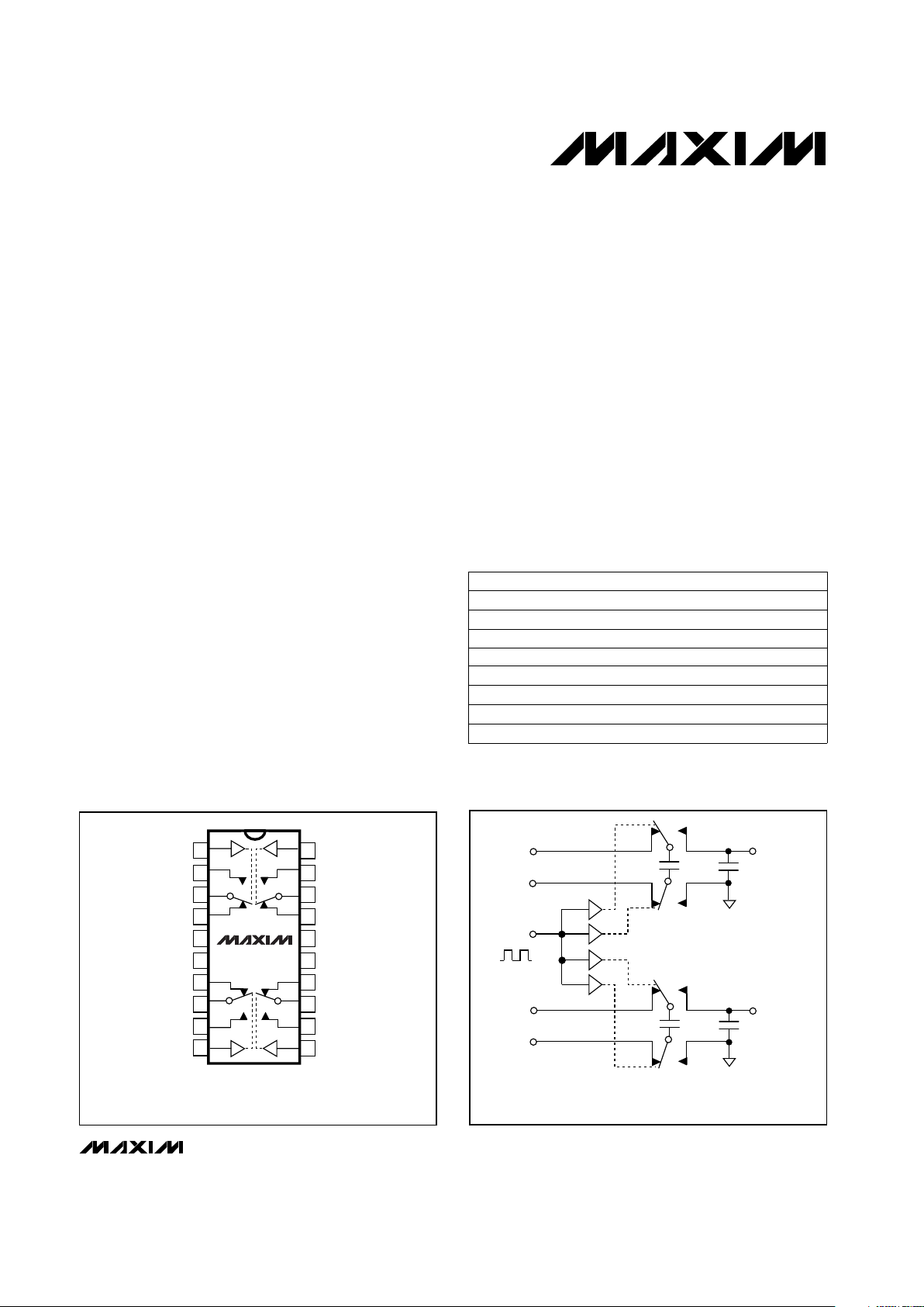
INPUTS
V
1
V
2
OSC
IN
V
3
V
4
FLYING CAPACITOR
LEVEL TRANSLATOR
(2-CHANNEL)
OUTPUTS
V
1
- V
2
V3 - V
4
__________Typical Operating Circuit
SWITCHES ARE SHOWN WITH LOGIC "0" INPUT
N.C. = NOT INTERNALLY CONNECTED
20
19
18
17
16
15
14
13
12
11
1
2
3
4
5
6
7
8
9
10
IN4
NO4
COM4
NC4
NC1
COM1
NO1
IN1
MAX333A
V+
N.C.
NC3
COM3
COM2
NC2
GND
V-
NO3
IN3
IN2
NO2
TOP VIEW
DIP/SO/TSSOP
__________________Pin Configuration
PART TEMP. RANGE PIN-PACKAGE
MAX333ACPP 0°C to +70°C 20 Plastic DIP
MAX333ACWP 0°C to +70°C 20 Wide SO
MAX333ACUP 0°C to +70°C 20 TSSOP
MAX333AEPP -40°C to +85°C 20 Plastic DIP
MAX333AEWP -40°C to +85°C 20 Wide SO
MAX333AEUP -40°C to +85°C 20 TSSOP
19-0189; Rev 1; 6/99
MAX333AC/D 0°C to +70°C Dice*
MAX333AMJP -55°C to +125°C 20 CERDIP
For free samples & the latest literature: http://www.maxim-ic.com, or phone 1-800-998-8800.
For small orders, phone 1-800-835-8769.
MAX333A
Precision, Quad, SPDT, CMOS Analog Switch
2 _______________________________________________________________________________________
ABSOLUTE MAXIMUM RATINGS
V+ to V- ..................................................................................44V
V
IN
, V
COM
, VNO, VNC......................................................V- to V+
(V
NO
- VNC) ............................................................................32V
V+ to Ground..........................................................................30V
V- to Ground..........................................................................-30V
Current, Any Terminal Except V
COM
, VNO, or VNC.............30mA
Continuous Current, V
COM
, VNO, or VNC............................20mA
Peak Current, V
COM
, VNO, or V
NC
(Pulsed at 1ms, 10% duty cycle max) ............................70mA
ESD ....................................................................................2000V
Continuous Power Dissipation (T
A
= +70°C) (Note 1)
Plastic DIP (derate above +70°C by 11.11mW/°C) .....889mW
SO (derate above +70°C by 10.00mW/°C)..................800mW
CERDIP (derate above +70°C by 11.11mW/°C)..........889mW
TSSOP (derate above +70°C by 7mW/°C) ..................559mW
Operating Temperature Ranges:
MAX333AC_ _ .....................................................0°C to +70°C
MAX333AE_ _ ..................................................-40°C to +85°C
MAX333AMJP................................................-55°C to +125°C
Storage Temperature Range .............................-65°C to +150°C
Lead Temperature (soldering, 10sec) .............................+300°C
ELECTRICAL CHARACTERISTICS—Dual Supplies
(GND = 0V, V+ = +15V, V- = -15V, TA= +25°C, unless otherwise noted.)
Note 1: Device mounted with all leads soldered to PC board.
Stresses beyond those listed under “Absolute Maximum Ratings” may cause permanent damage to the device. These are stress ratings only, and functional operation of the device at these or any other conditions beyond those indicated in the operational sections of the specifications is not implied. Exposure
to absolute maximum rating conditions for extended periods may affect device reliability.
PARAMETER SYMBOL
MIN TYP MAX
(Notes 2, 3)
UNITS
Input Voltage Low V
IL
V- 0.8 V
Negative Supply Current I- 0.01 1
µA
V+ 10 30
Input Voltage High V
IH
2.4 V+ V
Input Current I
IN
-1.0 0.0001 1.0 µA
Analog Signal Range V
COM, VNO,VNC
V- V+ V
Positive Supply Current I+ 0.05 0.25 mA
Supply Voltage Range
V+/V- ±4.5V ±20
V
On Circuit Resistance R
ON
20 35
Ω
On Resistance Match
Between Channels (Note 4)
R
ON
Ω
On Resistance Flatness
(Note 4)
R
ON
I
(NCorNO)
= -10mA, VD= 5V
or -5V, V+ =15V, V- = -15V
Ω
On Circuit Leakage
Current
I
COM
-0.75 0.75
nA
Off Circuit Leakage
Current
I
NC
or
I
NO
-0.25 0.01 0.25
nA
Turn-Off Time t
OFF
145 ns
Turn-On Time t
ON
175 ns
Break-Before-Make Time t
OPEN
10 ns
Off Capacitance C
OFF
5 pF
On Capacitance C
ON
5 pF
Charge Injection Q 210pC
OIRR 72 dB
CONDITIONS
VIN= 0V/5V,V+ = 16.5V, V- = -16.5V
Single supply, V- = GND
VIN= V-, V+
Figure 1
VIN= 0V/5V,V+ = 16.5V, V- = -16.5V
Dual supply, V+ = V-
CL= 10nF, V
GEN
= 0V,
R
GEN
= 0Ω, Figure 6
f = 1MHz, RL = 75Ω,
V
COM
= 2.3V
RMS
CCRR 78 dB
V
COM
= +10V, I
(NCorNO)
= 1mA;
V
COM
= -10V, I
(NCorNO)
= 1mA
2TA= +25°C
3
M
TA= +25°C
V
COM
= ±15.5V, V
NC
or VNO= +15.5V,
V+ = 16.5V, V- = -16.5V
V
COM
= ±15.5V V
NC
or VNO= +15.5V,
V+ = 16.5V, V- = -16.5V
M
M
TA= T
MIN
to T
MAX
TA= T
MIN
to T
MAX
C, E
C, E
C, E
TA= +25°C
45
4
5
-1.00 0.20 1.00
-0.50 0.02 0.05
Off Isolation
Crosstalk
I
(NCorNO)
= -10mA, VD= 10V
or -10V, V+ =15V, V- = -15V
POWER REQUIREMENTS
LOGIC INPUT
SWITCH
DYNAMIC
MAX333A
Precision, Quad, SPDT, CMOS Analog Switch
_______________________________________________________________________________________ 3
ELECTRICAL CHARACTERISTICS–DUAL SUPPLIES (continued)
(GND = 0V, V+ = +15V, V- = -15V, TA= T
MIN
to T
MAX
, unless otherwise noted.)
ELECTRICAL CHARACTERISTICS—Single Supply
(GND = 0V, V+ = +12V, V- = 0V, TA = +25°C, unless otherwise noted.)
PARAMETER
SYMBOL
MIN TYP MAX
(Notes 2, 3)
UNITS
On Circuit Resistance R
ON
45
Ω
Analog Signal Range V
COM
V- V+ V
Input Current I
IN
-1.0 0.0001 1.0 µA
On Circuit Leakage Current I
COM
-10 10
nA
On Circuit Leakage Current INCor I
NO
-6 6
nA
Input Voltage Low V
IL
V- 0.8 V
Input Voltage High V
IH
2.4 V+ V
CONDITIONS
VIN= V-, V+
PARAMETER
Off Circuit Leakage Current
SYMBOL
MIN TYP MAX
(Notes 2, 3)
I
NC
or
I
NO
0.25
UNITS
Input Current I
IN
nA
1 µA
Input Voltage High V
INHI
2.4 V+ V
Input Voltage Low V
INLO
0 0.8 V
Turn-Off Time
Analog Signal Range
V
COM
,
VNO, V
NC
V- V+ V
t
OFF
45 ns
Turn-On Time
On Circuit Resistance
t
ON
r
ON
35 75
90
Ω
On Circuit Leakage Current
ns
I
COM
0.75 nA
Break-Before-Make Time t
OPEN
510 ns
Off Isolation
Supply Voltage Range
OIRR 70 dB
Crosstalk CCRR 72 dB
V
+
10 30 V
Positive Supply Current l+ 0.25 mA
CONDITIONS
V
COM
= 11V
V
NC
or V
NO
= 1V
VIN= V+, 0V
Figure 1
V
COM
= 10V, I(
NC orNO)
= 1mA,
V
COM
= 1V, I(
NC orNO)
= 1mA
V
COM
= 11V, V
NC
or VNO= 0V
V
COM
= 1V, V
NC
or VNO= V+
f = 1MHz, RL= 75Ω, V
COM
= 2.3V
RMS
Single supply, V- = GND
V
COM
= 10V, I
(NC orNO)
= 1mA;
V
COM
= -10V, I
(NC orNO
= 1mA
V
COM
= ±15V, V
NC
or VNO= -15V,
V+ = 16.5V, V- = -16.5V
V
COM
= ±15V, V
NC
or VNO= -15V,
V+ = 16.5V, V- = -16.5V
C, E
C, E
C, E
M
M
M
45
-60 60
Note 2: The algebraic convention, whereby the most negative value is a minimum and the most positive is a maximum, is used in
this data sheet.
Note 3: Typical values are for design aid only, not guaranteed or subject to production testing.
Note 4: On resistance match between channels and flatness are guaranteed only with bipolar-supply operation.
LOGIC INPUT
SWITCH
DYNAMIC
SWITCH
INPUT
SUPPLY

MAX333A
Precision, Quad, SPDT, CMOS Analog Switch
4 _______________________________________________________________________________________
__________________________________________Typical Operating Characteristics
(TA = +25°C, unless otherwise noted).
45
5
-20 -10 10
ON RESISTANCE
vs. V
COM
AND POWER SUPPLY VOLTAGE
15
35
MAX333A-01
V
(V)
R
ON
(Ω)
020
25
40
10
30
20
50
A
B
C
D
A: V+ = 5V,
V- = -5V
B: V+ = 10V,
V- = -10V
C: V+ = 15V,
V- = -15V
D: V+ = 20V,
V- = -20V
5
-20 -10 10
ON RESISTANCE
vs. V
COM
AND TEMPERATURE
30
MAX333A-02
R
ON
(Ω)
020
20
10
25
15
35
V+ = 15V
V- = -15V
TA = +125°C
+85°C
+25°C
-55°C
20
05 15
ON RESISTANCE
vs. V
COM
AND TEMPERATURE
120
MAX333A-03
R
ON
(Ω)
10 20
80
40
100
60
140
V- = 0V
V+ = 5V
V+ = 10V
V+ = 15V
V+ = 20V
10
05 15
ON RESISTANCE
vs. V
COM
AND SINGLE SUPPLY
60
MAX333A-04
V
COM
(V)
R
ON
(Ω )
10 20
40
20
50
30
70
V+ = 12V
V- = 0V
TA = +125°C
TA = +85°C
TA = +25°C
-75
-20
CHARGE INJECTION vs. V
COM
50
MAX333A-07
V
COM
(V)
Q (pC)
020
0
-50
25
-25
75
-15 -10 -5 5 10 15
V
SUPPLY
= +15V
0.0001
-55
OFF LEAKAGE CURRENTS
vs. TEMPERATURE
10
MAX333A-05
TEMPERATURE (°C)
OFF LEAKAGE
+25 +125
0.1
0.001
1
0.01
100
V+ = 16.5V
V- = -16.5V
V
COM
= ±15V
V
NC
OR VNO = ±15V
0.0001
-55
ON LEAKAGE CURRENTS
vs. TEMPERATURE
10
MAX333A-06
TEMPERATURE (°C)
ON LEAKAGE
+25 +125
0.1
0.001
1
0.01
100
V+ = 16.5V
V- = -16.5V
V
COM
= ±15V
V
NC
OR VNO = ±15V
0.0001
-55
SUPPLY CURRENT vs. TEMPERATURE
10
MAX333A-08
TEMPERATURE (°C)
I+, I-, I
L
(µA)
+25 +125
0.1
0.001
1
0.01
100
I+ AT V+ = +16.5V
I- AT V+ = +16.5V

__________Applications Information
Operation with Supply Voltages
Other than ±15V
o
The main limitation of supply voltages other than ±15V is
a reduction in the analog signal range. The MAX333A
operates with ±5V to ±20V bipolar supplies. The
Typical Operating Characteristics
and graphs show typical on resistance for ±15V, ±10V, ±5 supplies.
Switching times increase by a factor of two or more for
±5V operation. The MAX333A can operate from +10V
to +24V unipolar supplies. It can be powered from a
single +10V to +24V supply, as well as from unbalanced
supplies such as +24V and -5V. Connect V- to 0V when
operating with a single supply.
Overvoltage Protection
Proper power-supply sequencing is recommended for
all CMOS devices. It is important not to exceed the
absolute maximum ratings because stresses beyond
the listed ratings may cause permanent damage to the
devices. Always sequence V+ on first, followed by VL,
V-, and logic inputs. If power-supply sequencing is not
possible, add two small signal diodes in series with the
supply pins (Figure 1). Adding the diodes reduces the
analog signal range to 1V below V+ and 1V below V-,
but low switch resistance and low leakage characteristics are unaffected.
MAX333A
Precision, Quad, SPDT, CMOS Analog Switch
_______________________________________________________________________________________ 5
PIN FUNCTION
15 Not Internally Connected
6 Ground
5 Negative Power Supply
4, 7, 14, 17 Normally Closed Switches
16 Positive Power Supply
1, 10, 11, 20 Logic-Level Inputs
2, 9, 12, 19 Normally Open Switches
3, 8, 13, 18 Common Switch Poles
NAME
N.C.
GND
V-
NC1-NC4
V+
IN1-IN4
NO1-NO4
COM1-COM4
_____________________Pin Description
tR < 20ns
t
F
< 20ns
50%
0V
+10V
LOGIC
INPUT
V-
-15V
300Ω
COM_
GND
(REPEAT TEST FOR IN2, IN3, AND IN4.)
V
IN
+10V
IN_
NO_
50%
t
OPEN
50% 50%
50% 50%
3V
t
OPEN
t
ON
t
OFF
t
ON
t
OFF
0V
-10V
V
COM
+15V
V+
NC_
-10V
SWITCH OUTPUT
Figure 2. Switching-Time Test Circuit
V
g
NO_
( OR NC_)
V+
COM_
V-
Figure 1. Overvoltage Protection Using Blocking Diodes
______________________________________________Test Circuits/Timing Diagrams

MAX333A
Precision, Quad, SPDT, CMOS Analog Switch
6 _______________________________________________________________________________________
CAPACITANCE
METER
NO_
OR NC_
COM_
GND
C
V-
-15V
IN_
0V, 2.4V
C
+15V
V+
50%
V
O1
V
O2
0.9V
O
+3V
0V
V
COM
0V
V
COM
LOGIC
INPUT
SWITCH
OUTPUT
SWITCH
OUTPUT
+15V
V+
NO
V-
-15V
CL INCLUDES FIXTURE AND STRAY CAPACITANCE.
LOGIC 0 INPUT.
GND
LOGIC
INPUT
0V
0.9V
O
t
D
t
D
R
L2
NC
C
L2
V
O2
V
O1
C
L1
R
L
= 1000Ω
CL = 35pF
COM_
V
COM
R
L1
IN_
V
GEN
GND
NC OR NO
C
L
10nF
V
O
-15V
V-
V+
R
GEN
V
O
IN_
ON
OFF
ON
∆V
O
Q = (∆V
O
)(CL)
COM_
+15V
IN_
Figure 3. Channel-Off Capacitance
Figure 5. Break-Before-Make
Figure 6. Charge Injection
CAPACITANCE
METER
NO
OR NC
COM_
GND
C
V-
-15V
IN_
0V,
2.4V
C
+15V
V+
Figure 4. Channel-On Capacitance
______________________________________________Test Circuits/Timing Diagrams

MAX333A
Precision, Quad, SPDT, CMOS Analog Switch
_______________________________________________________________________________________ 7
IN1
0V, 2.4V
SIGNAL
GENERATOR
+15V
C
ANALYZER
CH A
CH B
NC1 OR NO1
R
L
100Ω
GND
COM_
C
V-
-15V
REPEAT TESTS FOR OTHER CHANNELS
FREQUENCY
TESTED
1 MHz
SIGNAL
GENERATOR
AUTOMATIC
SYNTHESIZER
ANALYZER
TRACKING
SPECTRUM
ANALYZER
0V, 2.4V
IN_
NC_ OR NO_
50Ω
V+
COM1
IN_
0V,
2.4V
SIGNAL
GENERATOR
+15V
C
V+
ANALYZER
CH A
CH B
NC_
OR NO_
R
L
100Ω
GND
COM_
C
-15V
C = 5pF
FREQUENCY
TESTED
1 MHz
SIGNAL
GENERATOR
AUTOMATIC
SYNTHESIZER
ANALYZER
TRACKING
SPECTRUM
ANALYZER
OFF ISOLATION = 20LOG
V
COM
V
NC OR VNO
V-
Figure 7. Off-Isolation
Figure 8. Crosstalk
_________________________________Test Circuits/Timing Diagrams (continued)

Maxim cannot assume responsibility for use of any circuitry other than circuitry entirely embodied in a Maxim product. No circuit patent licenses are
implied. Maxim reserves the right to change the circuitry and specifications without notice at any time.
8
___________________Maxim Integrated Products, 120 San Gabriel Drive, Sunnyvale, CA 94086 (408) 737-7600
© 1999 Maxim Integrated Products Printed USA is a registered trademark of Maxim Integrated Products.
MAX333A
Precision, Quad, SPDT, CMOS Analog Switch
___________________Chip Topography
NO2
COM3
NC3
V+
NC4
NO3
IN3 IN2
NO4
COM4
0.139"
(3.53mm)
COM2
NC2
GND
V-
NC1
COM1
0.101"
(2.57mm)
IN4 IN1 NO1
TRANSISTOR COUNT: 145;
SUBSTRATE CONNECTED TO V+.
 Loading...