

For free samples & the latest literature: http://www.maxim-ic.com, or phone 1-800-998-8800.
For small orders, phone 1-800-835-8769.
General Description
The MAX3325 integrates a two-transmitter, two-receiver
RS-232 transceiver with an LCD supply plus temperature-compensated contrast control. It is intended for
small 3V instruments requiring a 5V supply for either
logic or an LCD display, an adjustable bias signal for
contrast, LCD temperature compensation, and an
RS-232 interface for serial communications.
The 5V supply is a regulated charge pump followed by
a low-dropout (LDO) linear regulator capable of supplying 11mA for the 5V LCD power.
The MAX3325 has an internal 6-bit digital-to-analog
converter (DAC) providing 64 contrast levels, plus an
internal temperature sensor that compensates the
LCD’s contrast for changes in ambient temperature.
The LCD contrast can be designed for any voltage
range from -5V to +2V.
The MAX3325’s 250kbps RS-232 transceiver meets all
EIA-232E specifications with input voltages from +3.0V
to +3.6V. Both the RS-232 section and the LCD supply
circuitry can be independently placed in shutdown, tailoring power consumption for battery-powered equipment. The MAX3325 is available in 28-pin SSOP and
narrow DIP packages.
Applications
PDAs and Palmtop Computers
Handy Terminals
GPS Receivers
Hand-Held Medical Equipment
Industrial Test Equipment
Features
♦ +3.0V to +3.6V Single-Supply Operation
♦ Provides 5.0V Regulated Output at 11mA in
3V Systems
♦ 6-Bit DAC with Up/Down Interface for LCD
Contrast Adjustment
♦ Selectable Positive or Negative LCD Bias
♦ Meets EIA-232E Specifications at 250kbps—
Guaranteed
♦ 1µA Shutdown Mode
♦ Uses Small 0.22µF Capacitors—No Inductors
Required
♦ Temperature Sensor for LCD Contrast
Compensation
♦ Simple, Flexible Design Procedure for a Broad
Range of LCD Displays
MAX3325
3V Dual RS-232 Transceiver with
LCD Supply and Contrast Controller
________________________________________________________________
Maxim Integrated Products
1
19-1573; Rev 0; 10/99
Typical Operating Circuit appears at end of data sheet.
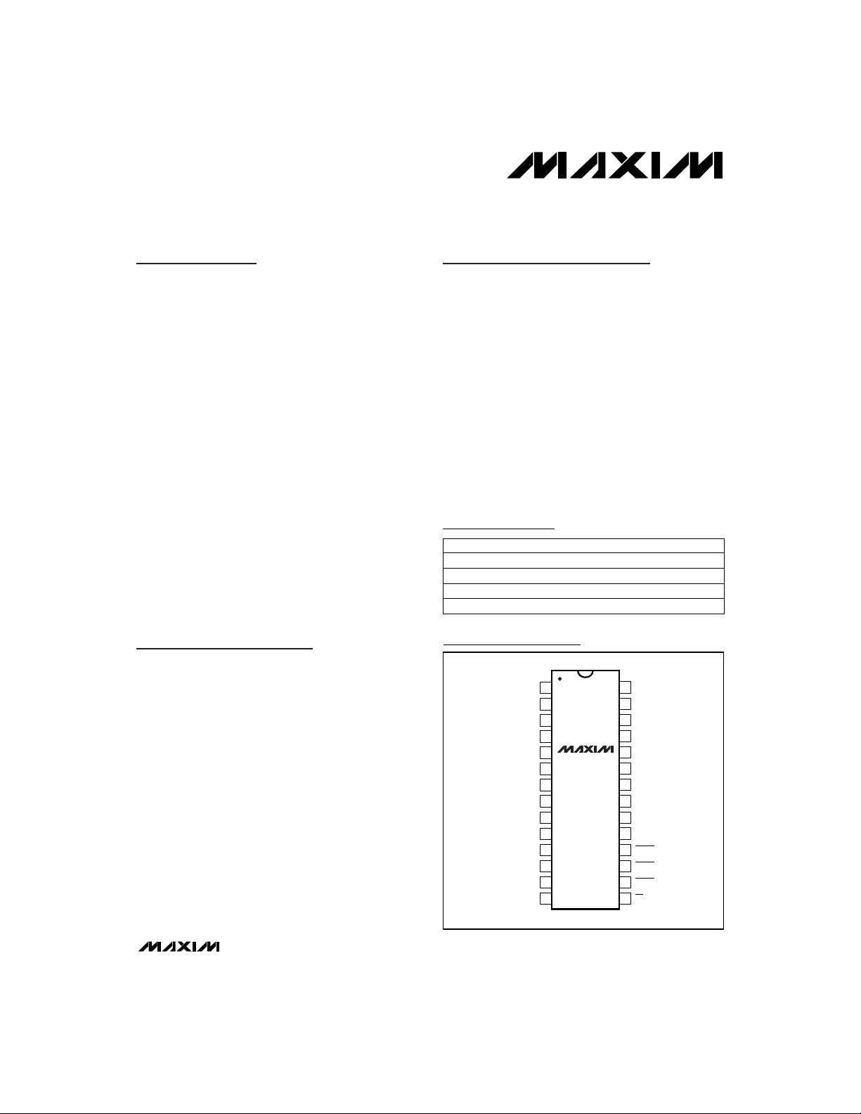
Pin Configuration
Ordering Information
PART
MAX3325CAI
MAX3325CNI
MAX3325EAI -40°C to +85°C
0°C to +70°C
0°C to +70°C
TEMP. RANGE PIN-PACKAGE
28 SSOP
28 Narrow Plastic DIP
28 SSOP
MAX3325ENI -40°C to +85°C 28 Narrow Plastic DIP
TOP VIEW
1
C2+
2
C2-
3
V-
4
R2IN
5
R1IN
R1OUT
R2OUT
LCD
TEMP
REF-
REF+
DAC
MAX3325
6
7
8
V
L
9
10
11
12
FB
13
14
SSOP/DIP
28
C1+
27
V+
26
V
DD
25
GND
24
C1-
23
REG
22
T1OUT
21
T2OUT
20
T1IN
19
T2IN
18
SD232
17
SDLCD
16
DOWN
15
UP
MAX3325
3V Dual RS-232 Transceiver with
LCD Supply and Contrast Controller
2 _______________________________________________________________________________________
ABSOLUTE MAXIMUM RATINGS
ELECTRICAL CHARACTERISTICS
(VDD= +3.0V to +3.6V, VL= +3.3V, circuit and components of Figure 1, TA= T
MIN
to T
MAX
, unless otherwise noted. Typical values
are at V
DD
= +3.3V, TA= +25°C.)
Stresses beyond those listed under “Absolute Maximum Ratings” may cause permanent damage to the device. These are stress ratings only, and functional
operation of the device at these or any other conditions beyond those indicated in the operational sections of the specifications is not implied. Exposure to
absolute maximum rating conditions for extended periods may affect device reliability.
VDD, VLto GND........................................................-0.3V to +6V
LCD, REF-, TEMP to GND.............................-6V to (V
DD
+ 0.3V)
V+ to GND (Note 1)..................................................-0.3V to +7V
V- to GND (Note 1)...................................................+0.3V to -7V
V+ to |V-| (Note 1) ................................................................+13V
REF+, FB, R_OUT to GND ............................-0.3V to (V
L
+ 0.3V)
Input Voltages
T_OUT, SDLCD, SD232, UP, DOWN to GND.......-0.3V to +6V
R_IN to GND....................................................................±25V
Output Voltages
T_OUT to GND.................................................................±13V
R_OUT to GND..........................................-0.3V to (V
L
+ 0.3V)
REG to GND.........................................................-0.3V to +6V
Short-Circuit Duration (T_OUT, REF+, REF-) .............Continuous
Continuous Output Current
REG.................................................................................75mA
LCD.................................................................................40mA
Continuous Power Dissipation
28-Pin SSOP (derate 9.52mW/°C above +70°C) .........762mW
28-Pin NDIP (derate 14.3mW/°C above +70°C) ........1143mW
Operating Temperature Range
MAX3325C_I.......................................................0°C to +70°C
MAX3325E_I ....................................................-40°C to +85°C
Storage Temperature Range.............................-65°C to +150°C
Lead Temperature (soldering, 10sec).............................+300°C
Note 1: V+ and V- can have maximum magnitudes of +7V, but their absolute difference cannot exceed 13V.
V
FB
= 0, CMOS input
3V < VDD< 3.6V
1 transmitter loaded with
5kΩ, TA= +25°C
I
TEMP
< 22µA
TA= +25°C
Guaranteed monotonic
No load
No load, VDD= VL= 3.3V, TA= +25°C
No load, VDD= VL= 3.3V, TA= +25°C
CONDITIONS
nA-10 0 10Input Leakage Current (Note 2)
mV-20 0 20Feedback Regulation Point
mA50Short-Circuit Current
mV650Line Regulation
4.7 5 5.3
mV/°C-18
TEMP Voltage Temperature
Coefficient
V-3.2TEMP Output
kΩ35 50 65Output Impedance
mV-15 0 10Zero-Scale Voltage
V1.13 1.2 1.27Full-Scale Voltage
Bits6
µA0.5 10VLSupply Current
mA24VDDSupply Current
UNITSMIN TYP MAXPARAMETER
SD232, SDLCD = GND; all input pins = GND or VDD;
V
DD
= VL= 3.3V; TA= +25°C
µA0.5 10VDDShutdown Supply Current
V
LCD
= -4.0V, load = 0 to -3mA mV20LCD Load Regulation (Note 3)
V
5
REG Output Voltage
0 < V
DAC
< V
REF
+, I
DAC
≤ 10µA
No load
V
CC
≥ 3.15V, I
REG
= 0 to
11mA
V
CC
≥ 3.0V, I
REG
= 0 to
7mA
DC CHARACTERISTICS
DIGITAL-TO-ANALOG CONVERTER
TEMPERATURE SENSOR
POSITIVE LINEAR REGULATOR
NEGATIVE LINEAR REGULATOR—LCD BIAS
Resolution
MAX3325
3V Dual RS-232 Transceiver with
LCD Supply and Contrast Controller
_______________________________________________________________________________________ 3
ELECTRICAL CHARACTERISTICS (continued)
(VDD= +3.0V to +3.6V, VL= +3.3V, circuit and components of Figure 1, TA= T
MIN
to T
MAX
, unless otherwise noted. Typical values
are at V
DD
= +3.3V, TA= +25°C.)
CONDITIONS UNITSMIN TYP MAXPARAMETER
LCD Line Regulation 3V < VDD< 3.6V, V
LCD
= -4.0V 10 mV
LCD Adjustment Range Load = -3mA -5 +2 V
Output Voltage R
REF
+ = 10kΩ 1.16 1.21 1.26 V
Load Regulation Load = 12µA to 62µA (sourcing current) 4 mV
Short-Circuit Current 5 mA
Output Voltage No load -1.14 -1.21 -1.28 V
Load Regulation Load = 0 to 50µA (sinking current) 35 mV
Short-Circuit Current 0.125 mA
Logic Threshold High 2 V
Logic Threshold Low 0.8 V
Input Current VIN= GND or V
DD
-1 1 µA
Output Voltage Low I
SINK
= 1.6mA 0.4 V
Output Voltage High I
SOURCE
= 1.0mA
0.8 · V
L
V
Input Voltage Range -25 +25 V
Input Threshold Low TA= +25°C, VDD= 3.3V 0.6 V
Input Threshold High TA= +25°C, VDD= 3.3V 2.4 V
Input Hysteresis 0.3 V
Input Resistance -15V < V
R_IN
< +15V, TA= +25°C 357kΩ
Output Voltage Swing All outputs loaded with 3kΩ to ground ±5 ±5.4 V
Output Resistance VDD= VL= V+ = V- = 0, V
OUT
= ±2V 300 10M Ω
Short-Circuit Current ±35 ±60 mA
Output Leakage Current
VDD= 0 or 3V to 3.6V, V
OUT
= ±12V, transmitters
disabled
±25 µA
POSITIVE REFERENCE VOLTAGE
NEGATIVE REFERENCE VOLTAGE
LOGIC INPUTS (SD232, SDLCD, T1IN, T2IN, UP, DOWN)
TRANSMITTER OUTPUTS
RECEIVER INPUTS
RECEIVER OUTPUTS
MAX3325
3V Dual RS-232 Transceiver with
LCD Supply and Contrast Controller
4 _______________________________________________________________________________________
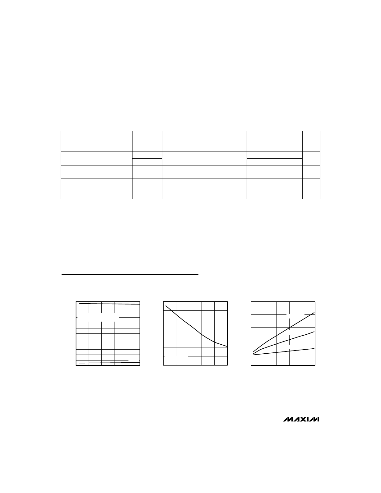
Typical Operating Characteristics
(VDD= VL= +3.3V, circuit and components of Figure 1, all transmitters loaded with 3kΩ,TA= +25°C, unless otherwise noted.)
TIMING CHARACTERISTICS
(VDD= +3.0V to +3.6V, VL= +3.3V, circuit and components of Figure 1, TA= T
MIN
to T
MAX
, unless otherwise noted. Typical values
are at V
DD
= +3.3V, TA= +25°C.)
Note 2: Guaranteed by design and not production tested.
Note 3: No load on REG or transmitter outputs.
t
PLH
300
PARAMETER SYMBOL MIN TYP MAX UNITS
Transition-Region Slew Rate 630V/µs
Transmitter Skew | t
PLH
- t
PHL
| 200 ns
Receiver Propagation Delay
Maximum Data Rate 250 kbps
t
PHL
300
ns
Receiver Skew | t
PLH
- t
PHL
| 300 ns
CONDITIONS
VDD= 3.3V, TA= +25°C, RL= 3kΩ to
7kΩ, C
L
= 150pF to 1000pF, measured
from +3V to -3V or -3V to +3V
RL= 3kΩ, CL= 1000pF, one transmitter
switching
Receiver input to receiver output,
CL= 150pF
TRANSMITTER OUTPUT VOLTAGE vs.
6
5
4
3
2
1
0
-1
-2
-3
-4
TRANSMITTER OUTPUT VOLTAGE (V)
-5
-6
LOAD CAPACITANCE
V
OUT+
T1 TRANSMITTING AT 250kbps
T2 TRANSMITTING AT 15.6kbps
V
OUT-
0 20001000 3000 4000 5000
LOAD CAPACITANCE (pF)
MAX3325toc01
SLEW RATE vs. LOAD CAPACITANCE
14
12
10
8
6
SLEW RATE (V/µs)
4
2
FOR DATA RATES
UP TO 250kbps
0
0 20001000 3000 4000 5000
LOAD CAPACITANCE (pF)
MAX3325toc02
SUPPLY CURRENT (mA)
CAPACITANCE (T1 = 20kbps)
50
40
30
20
10
0
0 1000 2000 3000 4000 5000
SUPPLY CURRENT vs. LOAD
T2 = 250kbps
T2 = 120kbps
T2 = 20kbps
LOAD CAPACITANCE (pF)
MAX3325toc03

MAX3325
3V Dual RS-232 Transceiver with
LCD Supply and Contrast Controller
_______________________________________________________________________________________
5
Typical Operating Characteristics (continued)
(VDD= VL= +3.3V, circuit and components of Figure 1, all transmitters loaded with 3kΩ and CL, TA= +25°C, unless otherwise noted.)
TRANSMITTER OUTPUTS EXITING
5V/div
0
SHUTDOWN OR POWERING UP
MAX3325toc04
SD232
T2OUT
LOOPBACK WAVEFORMS AT 120kbps
T1IN
5V/div
MAX3325toc05
T1IN
5V/div
LOOPBACK WAVEFORMS AT 250kbps
MAX3325toc06
2V/div
0
VCC = 3.3V
C1–C4 = 0.1µF
CL = 2500pF
6
5
4
(V)
3
REG
V
2
1
0
02010 30 40
40µs/div
V
vs. LOAD CURRENT
REG
VDD = +3V
LOAD CURRENT (mA)
VDD = +3.6V
VDD = +3.3V
T1OUT
MAX3325toc07
T1OUT/
R1IN
5V/div
R1OUT
5V/div
2
CL = 1000pF
6
5
4
(V)
3
REG
V
2
1
0
02010 30 40
µs/div
V
vs. LOAD CURRENT
REG
AND TEMPERATURE
TA = +25°C
LOAD CURRENT (mA)
TA = -40°C
TA = +85°C
T1OUT/
R1IN
5V/div
R1OUT
5V/div
MAX3325toc08
TEMP OUTPUT VOLTAGE (V)
CL = 1000pF
1µs/div
TEMP OUTPUT VOLTAGE
vs. TEMPERATURE
-1.5
-2.0
-2.5
-3.0
-3.5
-4.0
-4.5
-40 0 20-20 40 60 80 100
TEMPERATURE (°C)
MAX3325toc09

MAX3325
3V Dual RS-232 Transceiver with
LCD Supply and Contrast Controller
6 _______________________________________________________________________________________
NAME FUNCTION
1 C2+ Positive Terminal of Voltage-Inverting Charge-Pump Capacitor. Connect C2+ to C2- with a 0.22µF capacitor.
2 C2- Negative Terminal of Voltage-Inverting Charge-Pump Capacitor. Connect C2- to C2+ with a 0.22µF capacitor.
PIN
3 V- Output of Negative Charge Pump. Bypass V- to GND with a 0.22µF capacitor.
4, 5 R_IN RS-232 Receiver Inputs
10 TEMP
Output of Temperature Sensor. Connect TEMP to FB with a series resistor to compensate LCD contrast for
changing temperature. Bypass TEMP with a 0.22µF capacitor to GND.
9 LCD
Output of Negative Regulator. Connect LCD to FB with a series resistor. Bypass with a 0.47µF capacitor to
GND.
8 V
L
Supply Input for Receiver Outputs. Connect VLto the system logic supply voltage.
6, 7 R_OUT TTL/CMOS Receiver Outputs
15
UP DAC Adjust Input. A falling edge on UP increments the internal 6-bit DAC counter.
14 DAC Output of Internal 6-Bit DAC. Connect DAC to FB with a series resistor to adjust LCD voltage.
13 REF+ Output of Positive Reference, +1.2V. Bypass REF+ with a 0.22µF capacitor to GND.
12 FB Feedback Input for Negative Regulator. Regulates when FB is at zero (0).
11 REF- Output of Negative Reference, -1.2V. Bypass REF- with a 0.22µF capacitor to GND.
Pin Description
16
DOWN DAC Adjust Input. A falling edge on DOWN decrements the internal 6-bit DAC counter.
17
SDLCD
Active-Low Shutdown-Control Input for Both Regulators, References, DAC, and Temperature Sensors. Drive
SDLCD low to disable all analog circuitry. Drive high to enable the analog circuitry.
26 V
DD
+3.0V to +3.6V Supply Voltage. Bypass VDDwith a 0.22µF capacitor to GND.
25 GND Ground
24 C1- Negative Terminal of Voltage-Doubling Charge-Pump Capacitor. Connect C1- to C1+ with a 0.22µF capacitor.
18
SD232
Active-Low Shutdown-Control Input for Transmitter Outputs. Drive SD232 low to disable the RS-232
transmitters. Drive high to enable the transmitters.
23 REG Output of Positive Regulator. Bypass REG with a 4.7µF capacitor to GND.
21, 22 T_OUT RS-232 Transmitter Outputs
19, 20 T_IN TTL/CMOS Transmitter Inputs
28 C1+ Positive Terminal of Voltage-Doubling Charge-Pump Capacitor. Connect C1+ to C1- with a 0.22µF capacitor.
27 V+ Output of Positive Charge Pump. Bypass V+ to VDDwith a 0.22µF capacitor.

MAX3325
3V Dual RS-232 Transceiver with
LCD Supply and Contrast Controller
_______________________________________________________________________________________ 7
Figure 1. Application Circuit
C4
0.22µF
C3
0.22µF
C5
0.22µF
C1
0.22µF
C2
0.22µF
V-
V+
V
DD
UP
DOWN
SDLCD
C1+
C1C2+
C2-
GND
SD232
T1IN
MAX3325
6-BIT
DAC
REG
LCD
DAC
REF+
REF-
TEMP
T1OUT
4.7µF
R
FB
FB
10k
R
0.22µF
0.22µF
0.22µF
REF+8
R
R
R
OUT
REF-
TEMP
*
*
LCD
DISPLAY
0.47µF
*RESISTORS R
REF
T2IN
V
L
0.22µF
+ AND R
- ARE BOTH SHOWN, BUT ONLY ONE OR THE OTHER IS USED IN APPLICATION.
REF
R1OUT
R2OUT
5k
5k
T2OUT
R1IN
R2IN
C
L
C
L
R
L
R
L

Detailed Description
Dual Charge-Pump Voltage Converter
The MAX3325’s internal power supply consists of a regulated dual charge pump that provides output voltages
of +5.5V (doubling charge pump) and -5.5V (inverting
charge pump) over the 3.0V to 3.6V VDDrange. The
charge pump operates in discontinuous mode; if the
output voltages are less than 5.5V, the charge pump is
enabled; if the output voltages exceed 5.5V, the charge
pump is disabled. Each charge pump requires a flying
capacitor (C1, C2) and a reservoir capacitor (C3, C4)
to generate the V+ and V- supplies (Figure 1).
RS-232 Transmitters
The transmitters are inverting level translators that convert logic levels to ±5.0V EIA/TIA-232 levels. The
MAX3325 transmitters guarantee a 250kbps data rate
with worst-case loads of 3kΩ in parallel with 1000pF,
providing compatibility with PC-to-PC communication
software (such as LapLink™).
The MAX3325’s transmitters are disabled and the outputs are forced into a high-impedance state when the
RS-232 circuitry is in shutdown (SD232 = low). The
MAX3325 permits the outputs to be driven up to ±13V
in shutdown.
The transmitter inputs do not have pull-up resistors.
Connect unused inputs to GND or VDD.
RS-232 Receivers
The receivers convert RS-232 signals to logic output
levels. The VLpin controls the logic output high voltage.
The receiver outputs are always active, regardless of
the shutdown state.
Positive Voltage Regulator
The MAX3325 has a regulated +5V output suitable for
powering +5V LCD modules or other circuits. The output of the boost charge pump is regulated with an LDO
linear regulator. The REG output sources up to 11mA of
current to external circuitry.
Adjustable LCD Supply
The LCD output provides a flexible output voltage to
adjust the contrast of LCD modules. The output voltage
range is determined by the external circuitry connected
to LCD, FB, DAC, REF+ (or REF-, depending on contrast polarity). Additionally, the TEMP output can be
used to automatically compensate the contrast adjustment for temperature variance.
The LCD output is a linear regulator powered by the negative charge pump. It is capable of sinking up to 3mA of
current. Although the LCD regulator can be adjusted to
positive voltages, it is not capable of sourcing current. A
minimum output current of 100µA is required.
6-Bit DAC
The MAX3325’s DAC output is an unbuffered inverted
R2R structure with an output voltage range of 0 to
+1.2V. The DAC output impedance is typically 50kΩ,
and can be connected through a series resistor to the
FB input of the LCD regulator. An internal power-on
reset circuit sets the DAC to midscale on power-up.
DAC Control Inputs
The DAC code is controlled by UP and DOWN to adjust
the contrast of the LCD module. These inputs are
intended to interface to digital signals, but do not
include debounce circuitry. See the
Applications
sec-
tion. See Table 1 for the truth table.
Temperature Compensation
The MAX3325’s TEMP output is used to minimize deviation in LCD contrast level due to temperature changes.
The TEMP output is capable of sinking or sourcing up
to 22µA to the external resistor network.
Shutdown Mode
Supply current falls below 1µA in shutdown mode
(SDLCD = SD232 = low). When shut down, the device’s
charge pumps are shut off, V+ is pulled down to VDD,
V- is pulled to ground, and the transmitter outputs are
disabled (high impedance). The LCD section is also
powered down. The REG, LCD, and both reference outputs become high impedance. The time required to exit
shutdown is typically 100µs, as shown in the
Typical
Operating Characteristics
. However, the TEMP output
requires 50ms to fully stabilize. Connect SDLCD and
SD232 to VDDif the shutdown mode is not used. See
Table 2.
MAX3325
3V Dual RS-232 Transceiver with
LCD Supply and Contrast Controller
8 _______________________________________________________________________________________
LapLink is a trademark of Traveling Software.
X = Don’t care
Table 1. DAC Truth Table
Table 2. Shutdown Truth Table
UP
0
1
↓
DOWN
0
↓
1
FUNCTION
DAC set to midscale
DAC register decrements 1 count
DAC register increments 1 count
SDLCD
0
1
X
SD232
0
X
1
FUNCTION
Low-power shutdown mode
LCD bias and REG outputs enabled
RS-232 transmitters enabled

Applications Information
Capacitor Selection
The capacitor type used for C1–C4 is not critical for
proper operation; polarized or nonpolarized capacitors
can be used. Ceramic chip capacitors with an X7R
dielectric provide the best combination of performance,
cost, and size. The charge pump requires 0.22µF
capacitors for 3.3V operation. Do not use values smaller than those listed in Figure 1. Increasing the capacitor
values (e.g., by a factor of 2) reduces ripple on the
transmitter outputs, slightly reduces power consumption, and increases the available output current from
V
REG
and V
LCD
. C2, C3, and C4 can be increased
without changing C1’s value. However, do not
increase C1 without also increasing the values of
C2, C3, C4, and C5 to maintain the proper ratios.
When using the minimum required capacitor values,
make sure the capacitor value does not degrade excessively with temperature or voltage. This is typical of Y5V
and Z5U dielectric ceramic capacitors. If in doubt, use
capacitors with a larger nominal value, or specify X7R
dielectric. The capacitor’s equivalent series resistance
(ESR), which usually rises at low temperatures, influences
the amount of ripple on V+ and V-.
Power-Supply Decoupling
In most circumstances, a 0.22µF VDDbypass capacitor
(C5) is adequate. Choosing larger values for C5
increases performance and decreases the induced ripple on the VDDsupply line. Note that capacitor C2, connected to V+, is returned to C5. This connection also
improves the performance of the MAX3325. Locate all
bypass capacitors as close as possible to the IC. Keep
metal traces as wide as possible. Return all capacitor
ground connections directly to a solid-copper ground
plane.
Transmitter Outputs
when Exiting Shutdown
The
Typical Operating Characteristics
show the
MAX3325 transmitter outputs when exiting shutdown
mode. As they become active, the two transmitter outputs are shown going to opposite RS-232 levels (one
transmitter input is high, the other is low). Each transmitter is loaded with 3kΩ in parallel with 2500pF. The
transmitter outputs display no ringing or undesirable
transients as they come out of shutdown. Note that the
transmitters are enabled only when the magnitude of Vexceeds approximately -3V.
High Data Rates
The MAX3325 maintains the RS-232 ±5.0V minimum
transmitter output voltage even at high data rates.
Figure 1 shows a transmitter loopback test circuit. The
Typical Operating Characteristics
show loopback test
results at 120kbps and 250kbps. For 120kbps, all transmitters were driven simultaneously at 120kbps into RS232 loads in parallel with 1000pF. For 250kbps, a single
transmitter was driven at 250kbps, and all transmitters
were loaded with an RS-232 receiver in parallel with
1000pF.
Interconnection with
Lower Logic Voltages
The MAX3325 provides a separate supply for the logic
interface to optimize input and output levels. Connect
VLto the system’s logic supply voltage, and bypass it
with a 0.1µF capacitor to GND. If the logic supply is the
same as VDD, connect VLto VDD. The VLpin can be
operated from +1.8V to +5.0V to accommodate various
logic levels.
Setting V
LCD
Output Voltage
The LCD output can be configured in a variety of ways
to suit the requirements of the LCD display. First, determine the nominal voltage range that the LCD will
require for adequate contrast adjustment. If the display
requires temperature compensation for contrast,
include the TEMP output in all calculations. The output
voltage is defined by:
where code is the current digital code in the DAC, and
R
O
is the nominal DAC output impedance (50kΩ). The
other terms in the equation are due to external resistances connected to the indicated pins. A spreadsheet
program is an excellent tool for helping to select components and evaluate their effect on the output voltage
range.
Although the above equation has terms for both REF+
and REF- offset resistors, only one or the other is used.
Design Example
The first step in designing for a particular display is to
obtain the manufacturer’s device specifications for the
nominal values as well as the temperature characteristics.
For example, consider the Optrex DMC series of dot
matrix LCD modules. The manufacturer specifies a nominal contrast bias voltage of 6V at +25°C, where bias voltage is V
REG
- V
LCD
. The temperature coefficient needed
V =-R
code V
R + R
V
R
V
R
-3.3V - V (T - 25 C)
R
LCD FB
DAC
O DAC
REF+
REF+
REFREF-
TEMP
TEMP
⋅
⋅
()
++
+
°
MAX3325
3V Dual RS-232 Transceiver with
LCD Supply and Contrast Controller
_______________________________________________________________________________________ 9

to maintain the nominal contrast is -16mV/°C. In this case,
data for a spread of nominal bias voltages is not available, so a range of ±1V is chosen by experimentation.
Feedback Resistor (RFB)
The first step in designing the MAX3325 LCD bias is to
select a feedback resistor. This can be arbitrary, but
values between 220kΩ to 1MΩ are a good starting
point. We will choose 330kΩ. If the design can’t reach
its target range in later calculations, the feedback resistor can be adjusted accordingly.
DAC Output Resistor (R
OUT
)
Given the above criterion of a ±1V output range, the
DAC’s output should be multiplied by the ratio of the
desired output swing (±1V) divided by the available
output from the DAC (0 to 1.2V). Assuming that we’ve
used a 330kΩ feedback resistor, this corresponds to a
total DAC resistance of 200kΩ. Because the DAC has
an intrinsic output impedance of 50kΩ, set R
OUT
to
200kΩ - 50kΩ = 150kΩ.
Temperature Compensation Resistor (R
TEMP
)
Next, the temperature compensation resistor is selected. Because the MAX3325 regulates FB to virtual
ground, adding or removing the remaining resistors in
this design does not affect the transfer function set in
the previous section. The TEMP output has a temperature coefficient of -17.5mV per °C, and the LCD’s is
-16mV/°C. To scale these two values, multiply the feedback resistor (330kΩ) by the ratio of the TEMP coefficient divided by the display’s coefficient. For this
example, the result is 360kΩ.
Reference Resistance (R
REF_
)
To complete the design, the DC output is biased to the
final desired value at DAC midscale. Because the
previous steps concentrated on the transfer function
only, we now have a large offset of +1.94V. This is calculated from the entire equation, where the reference
resistors are assumed to be infinite, the DAC voltage is
+0.6V, and V
TEMP
is -3.2V. Connecting a 130kΩ resis-
tor from REF+ to FB forces V
LCD
to -1.1V, resulting in a
nominal contrast voltage (V
REG
- V
LCD
) of +6.1V. This
is close to the target value of +6V.
Actual Performance
The graph in Figure 2 shows the actual LCD display’s
data curve, along with the MAX3325’s performance
with various DAC codes. Note that changing the DAC
code does not affect the slope of the temperature compensation. If a wider scale of contrast adjustments is
desired, change the DAC output resistor, and readjust
the offset voltage.
Interfacing to the UP and DOWN Inputs
The UP and DOWN inputs to the MAX3325 are edgetriggered digital inputs. For proper operation, the signals must be standard logic signals. Mechanical switch
outputs, (toggle or membrane types) are unsuitable
and require proper debouncing before connecting to
the MAX3325. The best solution is to use the MAX6817
dual switch debouncer. This sends the correct signal
levels to the UP and DOWN inputs, and provides a
robust interface to the switch inputs. The UP and
DOWN inputs can be driven directly from a microprocessor.
System Considerations
Because the MAX3325 is the temperature transducer
for the LCD bias compensation, optimal performance is
obtained by placing the IC as close as possible to the
LCD.
MAX3325
3V Dual RS-232 Transceiver with
LCD Supply and Contrast Controller
10 ______________________________________________________________________________________
Figure 2. Design Example for Optrex DMC Display
Chip Information
TRANSISTOR COUNT: 1957
9
)
LCD
- V
REG
7
5
ACTUAL DISPLAY
CONTRAST VOLTAGE (V
MAX3325 LCD
BIAS CIRCUITRY
3
-40 0 20-20 40 60 80
TEMPERATURE (°C)
DAC CODE = 63
DAC CODE = 32
DAC CODE = 0

MAX3325
3V Dual RS-232 Transceiver with
LCD Supply and Contrast Controller
______________________________________________________________________________________ 11
Typical Operating Circuit
0.22µF
0.22µF
0.22µF
3V INPUT
TTL/CMOS
INPUTS
TTL/CMOS
OUTPUTS
V-
C1+
C1-
V+
V
DD
UP
DOWN
SDLCD
SD232
T1IN
T2IN
V
L
R1OUT
R2OUT
MAX3325
6-BIT
DAC
C2+
C2-
REG
POS
REG
LCD
NEG
REG
GND
FB
DAC
REF+
REF-
-1
TEMP
T
T1OUT
T2OUT
R1IN
R2IN
0.22µF
0.22µF
4.7µF
10k
0.33µF
RS-232
OUTPUTS
RS-232
INPUTS
5V AT 15mA
OUTPUT
LCD BIAS
(0 TO -5V)
0.33µF
0.47µF
LCD DISPLAY
MODULE
V
CC
V
EE
V
SS

MAX3325
3V Dual RS-232 Transceiver with
LCD Supply and Contrast Controller
Maxim cannot assume responsibility for use of any circuitry other than circuitry entirely embodied in a Maxim product. No circuit patent licenses are
implied. Maxim reserves the right to change the circuitry and specifications without notice at any time.
12
____________________Maxim Integrated Products, 120 San Gabriel Drive, Sunnyvale, CA 94086 408-737-7600
© 1999 Maxim Integrated Products Printed USA is a registered trademark of Maxim Integrated Products.
Package Information
SSOP.EPS
 Loading...