

Page 1
现货库存、技术资料、百科信息、热点资讯,精彩尽在鼎好!
General Description
The MAX3322E/MAX3323E 3.0V to 5.5V powered
EIA/TIA-232 and V.28/V.24 communications interfaces
are designed for multidrop applications with low power
requirements, high data-rate capabilities, and
enhanced electrostatic discharge (ESD) protection. All
RS-232 inputs and outputs are protected to ±15kV
using the IEC 1000-4-2 Air-Gap Discharge method,
±8kV using the IEC 1000-4-2 Contact Discharge
method, and ±15kV using the Human Body Model.
The MAX3322E/MAX3323E have pin-selectable
5kΩ/high-impedance RS-232 receivers. These devices
are capable of receiving data in high-impedance mode.
In multidrop applications, one receiver has a 5kΩ input
resistance, while the other receivers are high impedance to ensure the RS-232 standard is observed. Logic
control permits selection of the functional mode: high
impedance or RS-232 standard load. The transmitters
are enabled by logic control to allow the multiplexing of
the inputs to a single UART.
A proprietary low-dropout transmitter output stage
enables true RS-232 performance from a 3.0V to 5.5V
supply with a dual charge pump. The charge pump
requires only four small 0.1µF capacitors for operation
from a 3.3V supply. The MAX3322E/MAX3323E are
capable of running at data rates up to 250kbps while
maintaining RS-232-compliant output levels. The
MAX3322E/MAX3323E have a unique VLpin that allows
operation in mixed-logic voltage systems. Both input
and output logic levels are pin programmable through
the VLpin.
The MAX3322E is a 2Tx/2Rx device for hardware handshaking in standard RS-232 mode, and the MAX3323E
is a 1Tx/1Rx, required in most multidrop applications.
The MAX3322E is offered in a space-saving TSSOP
package. The MAX3323E is offered in 16-pin DIP and
space-saving TSSOP packages.
Applications
Bar-Code Scanners
Video Security
Industrial Data Acquisition
Data Splitters
Features
♦ Pin-Selectable 5kΩ/High-Impedance Receivers
♦ Transmitter Outputs Three-Stated by Logic
Control
♦ V
L
Pin for Compatibility with Mixed Voltage
Systems
♦ 1Tx/1Rx (MAX3323E) or 2Tx/2Rx (MAX3322E)
Versions
♦ 250kbps Data Rate
♦ 1µA Low-Power Shutdown
♦ High ESD Protection for RS-232 I/O Pins
±15kV—Human Body Model
±8kV—IEC 1000-4-2 Contact Discharge
±15kV—IEC 1000-4-2 Air-Gap Discharge
MAX3322E/MAX3323E
±15kV ESD-Protected, RS-232 Transceivers for
Multidrop Applications
________________________________________________________________ Maxim Integrated Products 1
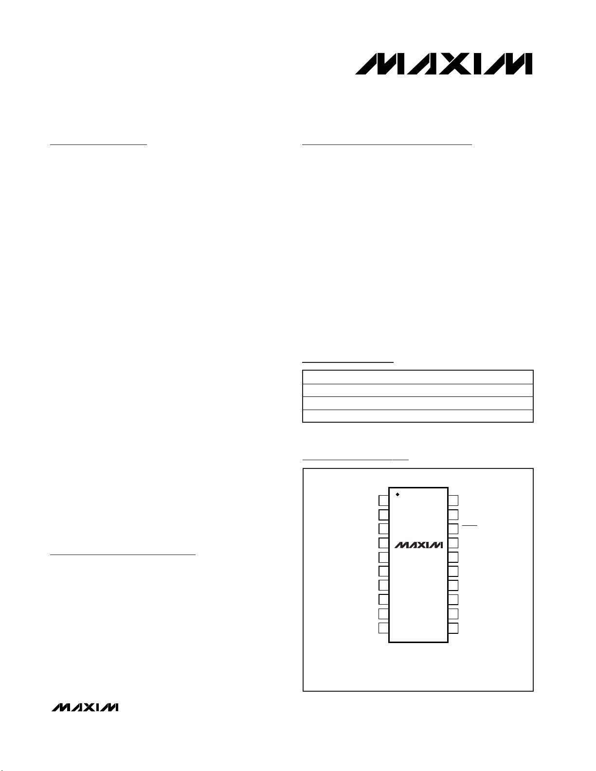
20
19
18
17
16
15
14
13
1
2
3
4
5
6
7
8
V
CC
GND
SHDN
V
L
C2+
C1-
V+
C1+
TOP VIEW
RENABLE
TXENABLE
TIN2
ROUT2RIN2
TOUT2
V-
C2-
12
11
9
10
TIN1
ROUT1RIN1
TOUT1
MAX3322E
TSSOP
Pin Configurations
Ordering Information
19-2667; Rev 1; 1/03
For pricing, delivery, and ordering information, please contact Maxim/Dallas Direct! at
1-888-629-4642, or visit Maxim’s website at www.maxim-ic.com.
PART TEMP RANGE
PIN-PACKAGE
MAX3322E EUP -40°C to +85°C 20 TSSOP
MAX3323E EUE -40°C to +85°C 16 TSSOP
MAX3323EEPE -40°C to +85°C 16 DIP
Pin Configurations continued at end of data sheet.
Typical Operating Circuit and Functional Diagram appear
at end of data sheet.
Page 2
MAX3322E/MAX3323E
±15kV ESD-Protected, RS-232 Transceivers for
Multidrop Applications
2 _______________________________________________________________________________________
ABSOLUTE MAXIMUM RATINGS
Stresses beyond those listed under “Absolute Maximum Ratings” may cause permanent damage to the device. These are stress ratings only, and functional
operation of the device at these or any other conditions beyond those indicated in the operational sections of the specifications is not implied. Exposure to
absolute maximum rating conditions for extended periods may affect device reliability.
All Voltages Referenced to GND
V
CC
, VL....................................................................-0.3V to +6V
V+ (Note 1) ....................................................(V
CC
- 0.3V) to +7V
V- (Note 1) ................................................................+0.3V to -7V
V+ + |V-| (Note 1) .................................................................+13V
Input Voltages
TIN_, RENABLE, TXENABLE,
SHDN .....................-0.3V to +6V
RIN_ ..................................................................................±25V
Output Voltages
TOUT_............................................................................±13.2V
ROUT_........................................................-0.3V to (V
L
+ 0.3V)
Short-Circuit Duration TOUT_ to GND........................Continuous
Continuous Power Dissipation (T
A
= +70°C)
16-Pin DIP (derate 10.5mW/°C above +70°C)............842mW
16-Pin TSSOP (derate 9.4mW/°C above +70°C) ........755mW
20-Pin TSSOP(derate 11mW/°C above +70°C) ..........879mW
Operating Temperature Range
MAX3322E/MAX3323E ...................................-40°C to +85°C
Junction Temperature..................................................... +150°C
Storage Temperature Range .............................-65°C to +150°C
Lead Temperature (soldering, 10s) .................................+300°C
DC ELECTRICAL CHARACTERISTICS
(VCC= 3.0V to 5.5V, VL= 1.65V to 5.5V, C1–C4 = 0.1µF, tested at +3.3V ±10%; C1 = 0.047µF, C2 = C3 = C4 = 0.33µF, tested at +5V
±10%; T
A
= T
MIN
to T
MAX
. Typical values are at VCC= VL= 3.3V and TA= +25°C, unless otherwise noted.)
PARAMETER
CONDITIONS
UNITS
DC CHARACTERISTICS
Supply Current Normal Operation
I
CC
SHDN = VL, no load 1 mA
Supply Current in Shutdown
)
SHDN = 0V, no load 1 10 µA
TRANSMITTER LOGIC INPUTS
Input Logic Threshold Low 0.4 V
VL ≤ 1.8V
Input Logic Threshold High
V
L
> 1.8V
V
Transmitter Input Hysteresis 0.2 V
Input Leakage Current I
IL
±1 µA
LOGIC INPUTS (TXENABLE, RENABLE, SHDN)
Input Logic Threshold Low 0.4 V
Input Logic Threshold High
V
Input Leakage Current
±1 µA
RECEIVER OUTPUTS
Output Leakage Current I
OL
Receivers disabled, SHDN = 0V
µA
I
OUT
= 1.6mA, VL > 1.8V 0.4
Output Voltage Low V
OL
I
OUT
= 1mA, VL ≤ 1.8V 0.4
V
I
OUT
= -1mA, VL > 1.8V
Output Voltage High V
OH
I
OUT
= -500µA, VL ≤ 1.8V
V
RECEIVER INPUTS
Input Voltage Range V
RIN
-25
V
VL = 1.65V
0.6
VL = 3.3V 0.6 1.2Input Threshold Low
V
L
= 5.0V 0.8 1.5
V
Note 1: V+ and V- can have maximum magnitudes of 7V, but their absolute difference cannot exceed 13V.
SYMBOL
MIN TYP MAX
I
CC(SHDN
VL - 0.4
2/3 x V
L
2/3 x V
L
VL - 0.4 VL - 0.1
VL - 0.4 VL- 0.1
0.25
±0.01
±0.01
+ 0.05 + 10
+25
Page 3
MAX3322E/MAX3323E
±15kV ESD-Protected, RS-232 Transceivers for
Multidrop Applications
_______________________________________________________________________________________ 3
DC ELECTRICAL CHARACTERISTICS (continued)
(VCC= 3.0V to 5.5V, VL= 1.65V to 5.5V, C1–C4 = 0.1µF, tested at +3.3V ±10%; C1 = 0.047µF, C2 = C3 = C4 = 0.33µF, tested at +5V
±10%; T
A
= T
MIN
to T
MAX
. Typical values are at VCC= VL= 3.3V and TA= +25°C, unless otherwise noted.)
PARAMETER
CONDITIONS
UNITS
VL = 1.65V 1 1.4
VL = 3.3V 1.5 2.4
Input Threshold High
V
L
= 5.0V 1.8 2.4
V
Input Hysteresis
V
RENABLE = 1 3 5 7 kΩ
Input Resistance R
IN
RENABLE = 0 or SHDN = 0V, RIN from -13V
to +13V
1MΩ
TRANSMITTER OUTPUTS
Output Voltage Swing
All transmitter outputs loaded with 3kΩ to
ground
±5
V
Output Resistance
V
CC
= V+ = V- = 0, TOUT_ = ±2V,
TXENABLE = 1
300
Ω
Output Short-Circuit Current V
OUT
= 0V
mA
Output Leakage Current V
OUT
= ±12V, transmitters disabled
µA
ESD PROTECTION
Human Body Model
IEC 1000-4-2 Air-Gap Discharge
RIN, TOUT
IEC 1000-4-2 Contact Discharge ±8
kV
TIMING CHARACTERISTICS
(VCC= 3.0V to 5.5V, VL= 1.65V to 5.5V, C1–C4 = 0.1µF, tested at +3.3V ±10%; C1 = 0.047µF, C2 = C3 = C4 = 0.33µF, tested at +5V
±10%; T
A
= T
MIN
to T
MAX
. Typical values are at VCC= VL= 3.3V and TA= +25°C, unless otherwise noted.)
PARAMETER
CONDITIONS
UNITS
Maximum Data Rate
R
L
= 3kΩ, CL = 1000pF, one transmitter
switching
kbps
t
PHL
Receiver Propagation Delay
t
PLH
RIN_ to ROUT_, CL = 30pF, VL = 3.3V,
Figure 2
ns
t
PHL
0.6
Transmitter Propagation Delay
t
PLH
TIN _ to TO U T_, RL = 3kΩ, C L = 1000p F,
Fi g ur e 1
0.7
µs
Time to Enter Three-State on Tx ( N ote 2) 10 50 µs
Time to Exit Three-State on Tx ( N ote 2) 3 50 µs
Time to Enable Resistor ( N ote 2) 0.4 10 µs
Time to Disable Resistor ( N ote 2) 0.2 10 µs
Time to Enter Shutdown 50 µs
Time to Exit Shutdown 50 µs
Transmitter Skew
ns
Receiver Skew 30 ns
Transition Region Slew Rate
R
L
= 3kΩ to 7kΩ, CL = 1000pF, measured
from +3V to -3V or vice versa
6 30 V/µs
Note 2: Guaranteed by design. Not production tested.
SYMBOL
MIN TYP MAX
0.35
±5.4
10M
±60
±25
±15
±15
SYMBOL
MIN TYP MAX
250
150
180
100
Page 4
MAX3322E/MAX3323E
±15kV ESD-Protected, RS-232 Transceivers for
Multidrop Applications
4 _______________________________________________________________________________________
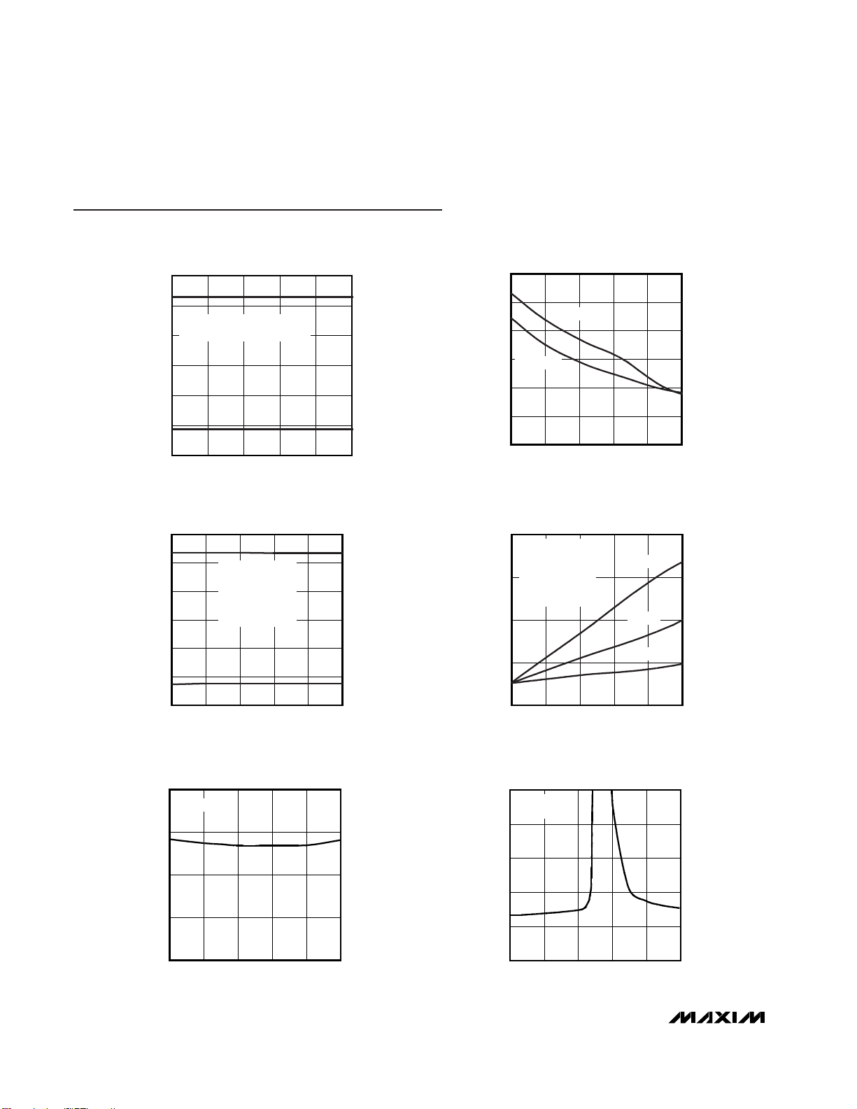
Typical Operating Characteristics
(VCC= 3.3V, VL= 3.3V, C1–C4 = 0.1µF, TA= +25°C.)
TRANSMITTER OUTPUT VOLTAGE
vs. LOAD CAPACITANCE
MAX3322E toc01
LOAD CAPACITANCE (pF)
OUTPUT VOLTAGE (V)
4000300020001000
-5.0
-2.5
0
2.5
5.0
7.5
-7.5
0 5000
DATA RATE = 250kbps
LOAD = 3kΩ IN PARALLEL WITH C
L
SLEW RATE
vs. LOAD CAPACITANCE
MAX3322E toc02
LOAD CAPACITANCE (pF)
SLEW RATE (V/µs)
4000300020001000
3
6
9
12
15
18
0
0 5000
SLEW RATE-
SLEW RATE+
TRANSMITTER OUTPUT VOLTAGE
vs. DATA RATE
MAX3322E toc03
DATA RATE (kbps)
OUTPUT VOLTAGE (V)
20015010050
-5.0
-2.5
0
2.5
5.0
7.5
-7.5
0 250
LOAD = 3kΩ, 1000pF
ONE TRANSMITTER
SWITCHING AT DATA
RATE, OTHER
TRANSMITTER
AT 1/8 DATA RATE
SUPPLY CURRENT
vs. LOAD CAPACITANCE
MAX3322E toc04
LOAD CAPACITANCE (pF)
SUPPLY CURRENT (mA)
4000300020001000
10
20
30
40
0
0 5000
250kbps
125kbps
40kbps
LOAD = 3kΩ
ONE TRANSMITTER
SWITCHING AT DATA
RATE, OTHER
TRANSMITTER
AT 1/8 DATA RATE
RECEIVER INPUT RESISTANCE
vs. INPUT VOLTAGE RANGE
MAX3322E toc05
V
RIN
(V)
RECEIVER INPUT RESISTANCE (kΩ)
155-5-15
4.75
5.00
5.25
5.50
4.50
-25 25
RENABLE = 1
RECEIVER INPUT RESISTANCE
vs. INPUT VOLTAGE RANGE
MAX3322E toc06
V
RIN
(V)
RECEIVER INPUT RESISTANCE (MΩ)
155-5-15
1
2
3
4
5
0
-25 25
RENABLE = 0
V
L
= 5V
Page 5

Detailed Description
The MAX3322E/MAX3323E are RS-232 transceivers for
multidrop applications (i.e., multiple-receiver operation).
The devices are pin selectable between standard RS-232
operation with 5kΩ input resistance receivers or highinput-impedance receivers. Receivers of the MAX3322E/
MAX3323E remain active in both modes of operation. In
multidrop applications, a selected receiver is set at a 5kΩ
input resistance, while the others are high-input impedance, maintaining RS-232 standards. Logic control permits selection of the functional mode: high impedance or
normal load. The transmitters are enabled by logic control
to allow transmission-line sharing.
The logic supply input (VL) controls the levels of the
system’s I/O and works from 1.65V to 5.5V, providing
compatibility with lower microprocessor I/O voltages.
The transmitters are inverting level translators that convert CMOS logic levels into RS-232-compatible levels.
They guarantee 250kbps with loads of RL= 3kΩ and C
L
= 1000pF. The transmitters are enabled or disabled
(three-stated) by the logic control TXENABLE, which
manages transmission-line sharing in multidrop applications. When TXENABLE is high, the transmitter is
enabled. When TXENABLE is low, the transmitter is put
in high-impedance state. The receivers can be used in
two conditions, selectable by the logic control RENABLE.
When RENABLE is high, the internal 5kΩ resistor is connected across receiver input and ground. When
RENABLE is low, the receiver input is high impedance,
while maintaining receiving capability.
In shutdown mode, all transmitter and receiver outputs
are three-stated, receiver inputs are in high impedance,
the charge pump is turned off, V+ decays to VCC, and
V- decays to ground. ESD protection structures are
incorporated in all pins to protect against ESD events
encountered during handling and assembly. The
receiver inputs and the transmitter outputs have ±15kV
ESD structure implementation.
MAX3322E/MAX3323E
±15kV ESD-Protected, RS-232 Transceivers for
Multidrop Applications
_______________________________________________________________________________________ 5
Pin Description
PIN
MAX3322E
NAME FUNCTION
1 1 C1+ Positive Terminal of the Voltage-Doubler Charge-Pump Capacitor
2 2 V+ +5.5V Generated by the Charge Pump
3 3 C1- Negative Terminal of the Voltage-Doubler Charge-Pump Capacitor
4 4 C2+ Positive Terminal of the Inverting Charge-Pump Capacitor
5 5 C2- Negative Terminal of the Inverting Charge-Pump Capacitor
6 6 V- -5.5V Generated by the Charge Pump
7, 9 7 TOUT_ Transmitter Output
8, 10 8 RIN_ Receiver Input
11, 13 9 ROUT_ Receiver Output
12, 14 10 TIN_ Transmitter Input
15 11
Transmitter Enable. Drive TXENABLE high to enable transmitter. Drive TXENABLE low
to put transmitter into high impedance.
16 12
Receiver Termination Enable. Drive RENABLE high for normal RS-232 5kΩ termination.
Drive RENABLE low to make receiver inputs high impedance. In either case, the
receiver and its output are enabled.
17 13 V
L
Logic-Level Supply. All CMOS inputs and outputs are referred to VL, which is from
1.65V to 5.5V.
18 14 SHDN
Shutdown Input. Drive SHDN low to put device into shutdown mode. Drive SHDN high
for normal operation. In shutdown, all transmitter and receiver outputs are in three-state;
receiver inputs are high impedance.
19 15 GND Ground
20 16 V
CC
+3V to +5.5V Input Voltage. Bypass VCC to GND with a 0.1µF capacitor.
MAX3323E
TXENABLE
RENABLE
Page 6

MAX3322E/MAX3323E
Dual Charge-Pump Voltage Converter
The MAX3322E/MAX3323Es’ internal power supply consists of a regulated dual charge pump that provides output voltages of +5.5V (doubling charge pump) and
-5.5V (inverting charge pump), regardless of the input
voltage (V
CC
), over a +3.0V to +5.5V range. The charge
pumps operate in a discontinuous mode: if the output
voltages are less than 5.5V, the charge pumps are
enabled; if the output voltages exceed 5.5V, the charge
pumps are disabled. Each charge pump requires a fly-
ing capacitor (C1, C2) and reservoir capacitor (C3, C4)
to generate the V+ and V- supplies. Because supply
voltages can vary from +3V up to +5.5V, the selection
of the capacitor values depends on the VCCvalue.
Table 2 shows minimum capacitor values.
RS-232 Transmitters
The transmitters are inverting level translators that convert CMOS-logic levels to 5.0V EIA/TIA-232 levels. The
transmitters are enabled or disabled (three-stated) by
the logic control TXENABLE, which manages transmission-line sharing in multidrop applications. When
TXENABLE is high, the transmitter is enabled. When
TXENABLE is low, the transmitter is put in a highimpedance state (see Table 1).
The MAX3322E/MAX3323Es’ transmitters guarantee a
250kbps data rate with worst-case loads of 3kΩ in parallel with 1000pF, providing compatibility with PC-to-PC
communication software (such as LapLink™).
Transmitters can be paralleled to drive multiple
receivers or mice. Figure 3 shows a complete system
connection.
RS-232 Receivers
MAX3322E/MAX3323E receivers convert RS-232 signals to CMOS-logic output levels. The unique feature of
the receivers is the switchable input resistance. The
receiver input resistance can be 5kΩ or high impedance. These two conditions are selectable by the logic
control RENABLE. When RENABLE is high, the 5kΩ
resistor is connected across the receiver input and
ground. When RENABLE is low, the receiver input is
high impedance, maintaining receiving capability. This
feature permits the design of multidrop applications,
which observe RS-232 interface standards.
±15kV ESD-Protected, RS-232 Transceivers for
Multidrop Applications
6 _______________________________________________________________________________________
LapLink is a trademark of Traveling Software.
INPUT
OUTPUT
+3V
V+
0V
V-
0V
t
PLH
t
PHL
Figure 1. Transmitter Propagation-Delay Timing
t
PHL
t
PLH
50%
V
CC
50%
+3V
50%
INPUT
OUTPUT
0V
50%
GND
Figure 2. Receiver Propagation-Delay Timing
MAX3322E
I/O
CHIP
WITH
UART
I/O
CHIP
POWER SUPPLY
V
L
V
L
CPU
RS-232
POWER-
MANAGEMENT
UNIT OR
KEYBOARD
CONTROLLER
SHDN
SHDN
Figure 3. Interface Under Control of PMU
Page 7

High-input impedance is guaranteed from -13.0V to
+13.0V, when the receiver is in high-input-impedance
mode. The receiver is able to withstand the RS-232
maximum input voltage of ±25V.
Shutdown Mode
Supply current falls to less than 10µA when the
MAX3322E/MAX3323E are placed in shutdown mode
(logic low). When in shutdown mode, the devices’
charge pumps are turned off, V+ decays to VCC, V- is
pulled to ground, the transmitter outputs and the
receiver outputs are disabled (high impedance), and
the receiver inputs are in high impedance (Table 1).
The device enters shutdown when VLor VCCis absent.
The time required to exit shutdown is typically 50µs, as
shown in Figure 4. Connect SHDN to VCCif shutdown
mode is not used.
VLLogic Supply Input
Unlike other RS-232 interface devices, in which the
receiver outputs swing between 0 and VCC, the
MAX3322E/MAX3323E feature a separate logic supply
input (VL) that sets V
OUT
for the receiver outputs and
sets thresholds for the transmit and shutdown inputs.
This feature allows a great deal of flexibility in interfacing to many types of systems with different logic levels.
Connect this input to the host logic supply (1.65V ≤ V
L
≤ 5.5V).
±15kV ESD Protection
To protect the MAX3322E/MAX3323E against ESD,
transmitters and receivers have extra protection against
static electricity to protect the device up to ±15kV. The
ESD structures withstand high ESD in all states: normal
operation, shutdown, and powered down. ESD protection can be tested in various ways; the transmitter and
receiver pins are characterized for protection to the following limits:
• ±15kV using the Human Body Model
• ±8kV using the IEC 1000-4-2 Contact Discharge
method
• ±15kV using the IEC 1000-4-2 Air-Gap method
Note: ESD performance depends on many conditions.
Contact Maxim for a reliability report that documents
test setup, test methodology, and test results.
Human Body Model
Figure 5 shows the Human Body Model, and Figure 6
shows the current waveform it generates when discharged into a low impedance. This model consists of
a 100pF capacitor charged to the ESD voltage of interest, which is then discharged into the test device
through a 1.5kΩ resistor.
MAX3322E/MAX3323E
±15kV ESD-Protected, RS-232 Transceivers for
Multidrop Applications
_______________________________________________________________________________________ 7
TXENABLE RENABLE SHDN TRANSMITTER OUTPUT
RECEIVER INPUT
1 1 0 High-Z High-Z High-Z
1 1 1 Active Enabled 5kΩ
1 0 0 High-Z High-Z High-Z
1 0 1 Active Enabled High-Z
0 1 0 High-Z High-Z High-Z
0 1 1 High-Z Enabled 5kΩ
0 0 0 High-Z High-Z High-Z
0 0 1 High-Z Enabled High-Z
Table 1. Tx/Rx Logic
50µs/div
T2
T1
5V/div
2V/div
VCC = 3.3V
C1–C4 = 0.1µF
Figure 4. Transmitter Outputs when Exiting Shutdown
RECEIVER OUTPUT
Page 8

MAX3322E/MAX3323E
IEC 1000-4-2
The IEC 1000-4-2 standard covers ESD testing and
performance of finished equipment; it does not refer
specifically to integrated circuits. The MAX3322E/
MAX3323E help the user design equipment that meets
level 4 of IEC 1000-4-2, without the need for additional
ESD-protection components. The major difference
between tests done using the Human Body Model and
IEC 1000-4-2 is a higher peak current in IEC 1000-4-2,
because series resistance is lower in the IEC 1000-4-2
model. Hence, the ESD withstand voltage measured to
IEC 1000-4-2 is generally lower than that measured
using the Human Body Model. Figure 7 shows the IEC
1000-4-2 model. Figure 8 shows the current waveform it
generates when discharged into a low impedance. The
Air-Gap Discharge test involves approaching the
device with a charged probe. The Contact Discharge
method connects the probe to the device before the
probe is energized.
Machine Model
The Machine Model for ESD tests all pins using a
200pF storage capacitor and zero discharge resistance. Its objective is to emulate the stress caused by
contact that occurs with handling and assembly during
manufacturing. All pins require this protection during
manufacturing. Therefore, after PC board assembly, the
Machine Model is less relevant to I/O ports.
Applications Information
The capacitor type used for C1–C4 is not critical for
proper operation; polarized or nonpolarized capacitors
can be used. The charge pump requires 0.1µF capacitors for 3.3V operation. For other supply voltages, see
Table 2 for required capacitor values. Do not use values smaller than those listed in Table 2. Increasing the
capacitor values (e.g., by a factor of 2) reduces ripple
±15kV ESD-Protected, RS-232 Transceivers for
Multidrop Applications
8 ____________________________________________________
CHARGE-CURRENT-
LIMIT RESISTOR
DISCHARGE
RESISTANCE
STORAGE
CAPACITOR
C
s
100pF
R
C
1MΩ
R
D
1.5kΩ
HIGH-
VOLTAGE
DC
SOURCE
DEVICE
UNDER
TEST
Figure 5. Human Body ESD Test Model
IP 100%
90%
36.8%
t
RL
TIME
t
DL
CURRENT WAVEFORM
PEAK-TO-PEAK RINGING
(NOT DRAWN TO SCALE)
I
r
10%
0
0
AMPERES
Figure 6. Human Body Model Current Waveform
CHARGE-CURRENT-
LIMIT RESISTOR
DISCHARGE
RESISTANCE
STORAGE
CAPACITOR
C
s
150pF
R
C
50Ω to 100Ω
R
D
330Ω
HIGH-
VOLTAGE
DC
SOURCE
DEVICE
UNDER
TEST
Figure 7. IEC 1000-4-2 ESD Test Model
tr = 0.7ns TO 1ns
30ns
60ns
t
100%
90%
10%
I
PEAK
I
Figure 8. IEC 1000-4-2 ESD Generator Current Waveform
Page 9

on the transmitter outputs and slightly reduces power
consumption. The values of C2, C3, and C4 can be
increased without changing C1’s value. However, do
not increase C1’s value without also increasing the val-
ues of C2, C3, and C4 to maintain the proper ratios (C1
to the other capacitors).
When using the minimum required capacitor values,
make sure the capacitor value does not degrade
excessively with temperature. If in doubt, use capacitors with a larger nominal value. The capacitor’s equivalent series resistance (ESR), which usually rises at low
temperatures, influences the amount of ripple on V+
and V-.
Multidrop Applications
The MAX3323E connects to the RS-232 serial port of
computer peripherals such as a bar-code scanner,
video security controls, industrial multimeters, etc., and
allows multiple devices to share the same communication cable connected to a PC.
Figure 9 shows a PC UART transmitting to a single
receiver with a 5kΩ termination resistor while the other
receivers remain in a high-impedance state. When the
receiver inputs are high impedance, they remain active
and maintain receiving capability. This feature permits
the design of multidrop applications, which observe the
RS-232 interface standard.
Transmitters are enabled and disabled through
TXENABLE, allowing the sharing of a single bus line.
Transmitters are high impedance when disabled. The
host PC’s transmitter stays enabled at all times. Only
one peripheral transmitter remains enabled at any time.
If the host PC wants to communicate with another
peripheral, it first must tell the current peripheral to
deassert its transmitter.
MAX3322E/MAX3323E
±15kV ESD-Protected, RS-232 Transceivers for
Multidrop Applications
_______________________________________________________________________________________ 9
MAX3323E
PC
UART
5kΩ
PERIPHERAL
CONTROL WITH UART
MAX3323E
5kΩ
PERIPHERAL
CONTROL WITH UART
MAX3323E
5kΩ
PERIPHERAL
CONTROL WITH UART
Figure 9. Multidrop Application
VCC (V) C1 (µF)
3.0 to 3.6 0.1 0.1
4.5 to 5.5 0.047 0.33
3.0 to 5.5 0.22 1
Table 2. Minimum Required Capacitor
Values
C2, C3, C4 (µF)
Page 10

MAX3322E/MAX3323E
Power-Supply Decoupling
In most circumstances, a 0.1µF bypass capacitor is adequate. In applications sensitive to power-supply noise,
decouple V
CC
to ground with a capacitor of the same
value as charge-pump capacitor C1. Connect bypass
capacitors as close to the IC as possible.
High Data Rates
The MAX3322E/MAX3323E maintain the RS-232 ±5.0V
minimum transmitter output voltage even at high data
rates. Figure 10 shows a transmitter loopback test circuit. Figure 11 shows a loopback test result at
125kbps, and Figure 12 shows the same test at
250kbps. For Figure 11, all transmitters were driven
simultaneously at 125kbps into RS-232 loads in parallel
with 1000pF. For Figure 12, a single transmitter was driven at 250kbps, and all transmitters were loaded with
an RS-232 receiver in parallel with 1000pF.
Interconnection with 3V and 5V Logic
The MAX3322E/MAX3323E can directly interface with
various 5V logic families, including ACT and HCT
CMOS. The logic voltage power-supply pin VLsets the
output voltage level of the receivers and the input
thresholds of the transmitters.
±15kV ESD-Protected, RS-232 Transceivers for
Multidrop Applications
10 ______________________________________________________________________________________
MAX3323E
R_OUT
GND
T_IN
C2-
5
C2+
4
C1-
3
C1+
1
R_IN
5kΩ
T_OUT
V-
6
V+
2
V
CC
SHDN
C4
0.1µF
1000pF
C3
0.1µF
C1
0.1µF
0.1µF
C2
0.1µF
+3.3V
Figure 10. Loopback Test Circuit
MAX3322E fig11
2µs/div
T1IN
5V/div
T1OUT
5V/div
R1OUT
5V/div
VCC = 3.3V
Figure 11. Loopback Test Results at 125kbps
MAX3322E fig12
1µs/div
T1IN
5V/div
T1OUT
5V/div
R1OUT
5V/div
VCC = 3.3V
Figure 12. Loopback Test Results at 250kbps
Page 11

MAX3322E/MAX3323E
±15kV ESD-Protected, RS-232 Transceivers for
Multidrop Applications
______________________________________________________________________________________ 11
MAX3322E
R1OUT11
8
19
GND
RS-232
OUTPUTS
TTL/CMOS
INPUTS
T2IN
14
15
16
T1IN
ENABLE
CONTROL
12
C2-
5
C2+
4
C1-
3
C1+
1
R1IN
10
5kΩ
V
L
V
L
5kΩ
7
T1OUT
T2OUT
9
V-
6
V+
2
V
CC
SHDN
V
L
C4
0.1µF
C3
0.1µF
20
18
17
C1
0.1µF
C2
0.1µF
+3.3V
RS-232
INPUTS
TTL/CMOS
OUTPUTS
TXENABLE
RENABLE
R2OUT13 R2IN
Typical Operating Circuit
16
15
14
13
12
11
10
9
1
2
3
4
5
6
7
8
C1+
V
CC
GND
SHDN
V
L
RENABLE
TXENABLE
TIN1
ROUT1
TOP VIEW
MAX3323E
TSSOP/DIP
V+
C1-
V-
C2+
C2-
TOUT1
RIN1
Pin Configurations (continued)
Chip Information
TRANSISTOR COUNT: 1294
PROCESS: BiCMOS
MAX3322E
MAX3323E
CHARGE PUMP
HIGH
IMPEDANCE
V
L
V+
V-
C1+
V+
V
CC
V
L
ROUT
RENABLE
TIN
TXENABLE
SHDN
V-
RIN
5kΩ
TOUT
C1-
C2+
C2-
Functional Diagram
Page 12

Package Information
(The package drawing(s) in this data sheet may not reflect the most current specifications. For the latest package outline information,
go to www.maxim-ic.com/packages
.)
MAX3322E/MAX3323E
±15kV ESD-Protected, RS-232 Transceivers for
Multidrop Applications
12 ______________________________________________________________________________________
Page 13

MAX3322E/MAX3323E
±15kV ESD-Protected, RS-232 Transceivers for
Multidrop Applications
Maxim cannot assume responsibility for use of any circuitry other than circuitry entirely embodied in a Maxim product. No circuit patent licenses are
implied. Maxim reserves the right to change the circuitry and specifications without notice at any time.
Maxim Integrated Products, 120 San Gabriel Drive, Sunnyvale, CA 94086 408-737-7600 ____________________ 13
© 2003 Maxim Integrated Products Printed USA is a registered trademark of Maxim Integrated Products.
Package Information (continued)
(The package drawing(s) in this data sheet may not reflect the most current specifications. For the latest package outline information,
go to www.maxim-ic.com/packages
.)
 Loading...