

Page 1
现货库存、技术资料、百科信息、热点资讯,精彩尽在鼎好!
General Description
The MAX3314E is a ±5V-powered EIA/TIA-232-compatible interface. It has one transmitter and one receiver in
a flow-through architecture. The transmitter output and
the receiver input are protected to ±15kV using IEC
1000-4-2 Air-Gap Discharge, ±8kV using IEC 1000-4-2
Contact Discharge, and ±15kV using the Human Body
Model.
The transmitter has a low-dropout output stage providing minimum RS-232-compatible ±3.7V output levels
while driving 3kΩ and 1000pF at 460kbps. Both +5V
and -5V must be supplied externally.
The MAX3314E has a SHDN function that reduces supply current to 1µA. The transmitter is disabled and put
into tristate while the receiver remains active.
The MAX3314E is available in 8-pin µMAX, SOT23, and
SO packages.
________________________Applications
Digital Cameras
PDAs
GPS
POS
Telecommunications
Handy-Terminals
Set-Top Boxes
Features
♦ ESD Protection for RS-232 I/O Pins
±15kV—Human Body Model
±8kV—IEC 1000-4-2 Contact Discharge
±15kV—IEC 1000-4-2 Air-Gap Discharge
♦ 1µA Low-Power Shutdown with Receiver Active
♦ 30µA Operating Supply Current
♦ 460kbps Guaranteed Data Rate
♦ 8-Pin SOT23 Package
♦ ±3.7V RS-232-Compatible Levels
MAX3314E
±15kV ESD-Protected, 460kbps, 1µA,
RS-232-Compatible Transceiver
________________________________________________________________ Maxim Integrated Products 1
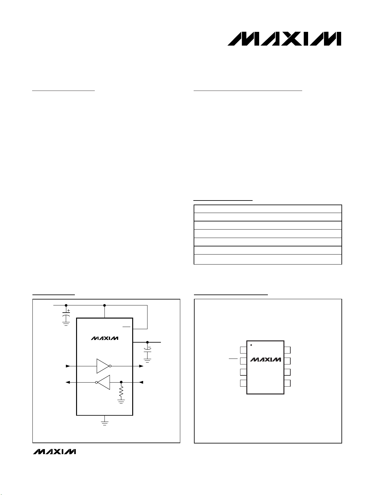
Pin Configuration
C
BYPASS
0.1µF
2
7
1
8
5
6
4
3
SHDN
V-
TOUT
RIN
TIN
ROUT
V
CC
GND
5kΩ
+5V
MAX3314E
CAPACITORS MAY BE POLARIZED OR NONPOLARIZED.
0.1µF
-5V
Typical Operating Circuit
19-1696; Rev 1; 3/01
Ordering Information
For pricing, delivery, and ordering information, please contact Maxim/Dallas Direct! at
1-888-629-4642, or visit Maxim’s website at www.maxim-ic.com.
PART TEMP. RANGE PIN-PACKAGE
MAX3314ECKA-T 0°C to +70°C 8 SOT23-8
MAX3314ECUA 0°C to +70°C 8 µMAX
MAX3314ECSA 0°C to +70°C 8 SO
MAX3314EEKA-T -40°C to +85°C 8 SOT23-8
MAX3314EEUA -40°C to +85°C 8 µMAX
MAX3314EESA -40°C to +85°C 8 SO
TOP VIEW
1
V
CC
2
SHDN
ROUT
MAX3314E
3
4
SOT23/µMAX/SO
87GND
V-
RIN
6
TOUTTIN
5
Page 2
MAX3314E
±15kV ESD-Protected, 460kbps, 1µA,
RS-232-Compatible Transceiver
2 _______________________________________________________________________________________
ABSOLUTE MAXIMUM RATINGS
Stresses beyond those listed under “Absolute Maximum Ratings” may cause permanent damage to the device. These are stress ratings only, and functional
operation of the device at these or any other conditions beyond those indicated in the operational sections of the specifications is not implied. Exposure to
absolute maximum rating conditions for extended periods may affect device reliability.
VCCto GND.............................................................-0.3V to +6V
V- to GND ...............................................................+0.3V to -6V
Input Voltages
TIN, SHDN to GND ...............................................-0.3V to +6V
RIN to GND ......................................................................±25V
Output Voltages
TOUT to GND................................................................±13.2V
ROUT .................................................…-0.3V to (V
CC
+ 0.3V)
Short-Circuit Duration
TOUT to GND .........................................................Continuous
Continuous Power Dissipation
8-Pin SOT23 (derate 9.7mW/°C above +70°C)...........777mW
8-Pin µMAX (derate 4.1mW/°C above +70°C) ............300mW
8-Pin SO (derate 5.88mW/°C above +70°C)...............471mW
Operating Temperature Ranges
MAX3314EC_A ..................................................0°C to +70°C
MAX3314EE_A................................................-40°C to +85°C
Junction Temperature.....................................................+150°C
Storage Temperature Range ............................-65°C to +150°C
Lead Temperature (soldering, 10s) ................................+300°C
ELECTRICAL CHARACTERISTICS
(VCC= +5V, V- = -5V, TA= T
MIN
to T
MAX
. Typical values are at TA= +25°C.)
PARAMETER SYMBOL CONDITIONS MIN TYP MAX UNITS
DC CHARACTERISTICS
P osi ti ve S up p l y Op er ati ng Rang e V
4.75 5 5.25 V
CC
N egati ve S up p l y O p er ating Range V- -4.75 -5 -5.25 V
Positive Supply Current SHDN = V
Negative Supply Current SHDN = V
, no load 30 100 µA
CC
, no load 15 30 µA
CC
Shutdown Supply Current SHDN = GND 1 10 µA
LOGIC INPUTS (TIN, SHDN)
Input Logic Threshold Low V
Input Logic Threshold High V
0.8 V
IL
2.4 V
IH
Transmitter Input Hysteresis 0.5 V
Input Leakage Current ±0.01 µA
RECEIVER OUTPUT
Output Voltage Low V
Output Voltage High V
OL
OH
I
= 1.6mA 0.4 V
OUT
I
= -1.0mA
OUT
RECEIVER INPUT
Input Threshold Low V
Input Threshold High V
0.8 V
IL
2.4 V
IH
Input Hysteresis 0.5 V
Input Resistance 5 kΩ
TRANSMITTER OUTPUT
Output Voltage Swing Tr ansm i tter outp ut l oad ed w i th 3kΩ to g r ound ±3.7 V
Output Resistance (Note 1) V
= V- = 0, transmitter output = ±2V 300 Ω
CC
Output Short-Circuit Current ±60 mA
Output Leakage Current V
= ±12V, transmitter disabled 25 µA
OUT
ESD PROTECTION (Transmitter Output, Receiver Input)
Human Body Model ±15
ESD-Protection Voltage
IEC 1000-4-2 Air-Gap Discharge ±15
IEC 1000-4-2 Contact Discharge ±8
V
- 0.3
CC
V
CC
- 0.1
V
kV
Page 3
MAX3314E
±15kV ESD-Protected, 460kbps, 1µA,
RS-232-Compatible Transceiver
_______________________________________________________________________________________ 3
Note 1: Not tested, guaranteed by design.
TIMING CHARACTERISTICS
(VCC= +5V, V- = -5V, TA= T
MIN
to T
MAX
. Typical values are at TA= +25°C.)
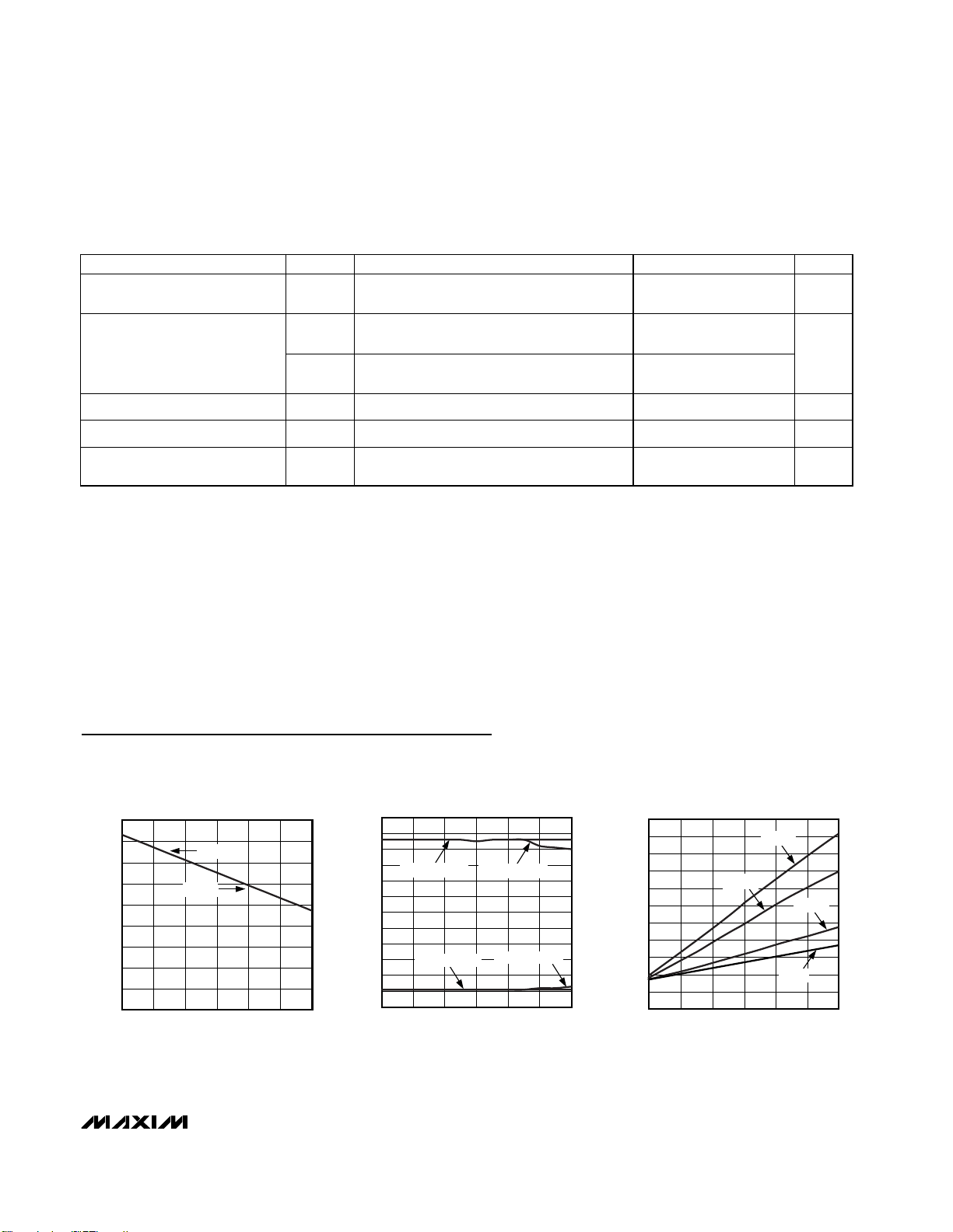
Typical Operating Characteristics
(VCC= +5V, V- = -5V, 250kbps data rate, transmitter loaded with 3kΩ and CL, TA= +25°C, unless otherwise noted.)
PARAMETER SYMBOL CONDITIONS MIN TYP MAX UNITS
Maximum Data Rate
Receiver Propagation Delay
Transmitter Skew 100 ns
Receiver Skew
Transition Region Slew Rate
R
= 3kΩ, C
L
switching
t
PLH
t
PHL
Receiver input to receiver output,
= 150pF
C
L
Receiver input to receiver output,
= 150pF
C
L
50 ns
RL = 3kΩ to 7kΩ, CL = 150pF to 1000pF,
measured from +3V to -3V or -3V to +3V
= 1000pF, transmitter
L
460
0.15
0.15
8 V/µs
kbps
µs
SLEW RATE vs. LOAD CAPACITANCE
9
8
7
6
5
4
SLEW RATE (V/µs)
3
2
1
0
0 1000500 1500 2000 2500 3000
-SLEW
+SLEW
LOAD CAPACITANCE (pF)
TRANSMITTER OUTPUT VOLTAGE
6
5
MAX3314E-01
4
3
20kbps/120kbps
2
1
0
-1
-2
-3
-4
TRANSMITTER OUTPUT VOLTAGE (V)
-5
-6
500
0 1000 1500 2000 2500 3000
vs. LOAD CAPACITANCE
460kbps/250kbps
20kbps/120kbps
LOAD CAPACITANCE (pF)
460kbps/250kbps
MAX3314E-02
SUPPLY CURRENT (mA)
5.5
5.0
4.5
4.0
3.5
3.0
2.5
2.0
1.5
1.0
0.5
0
0 500 1000 1500 2000 2500 3000
SUPPLY CURRENT
vs. LOAD CAPACITANCE
250kbps
LOAD CAPACITANCE (pF)
460kbps
MAX3314E-03
120kbps
20kbps
Page 4

MAX3314E
±15kV ESD-Protected, 460kbps, 1µA,
RS-232-Compatible Transceiver
4 _______________________________________________________________________________________
Detailed Description
RS-232-Compatible Drivers
The transmitter is an inverting level translator that converts CMOS-logic levels to ±3.7V EIA/TIA-232-compatible levels. It guarantees data rates up to 460kbps with
worst-case loads of 3kΩ in parallel with 1000pF. When
SHDN is driven low, the transmitter is disabled and put
into tristate. The transmitter input does not have a pullup resistor. Connect to ground if unused.
RS-232-Compatible Receivers
The MAX3314E’s receiver converts RS-232 signals to
CMOS-logic output levels. The receiver is rated to
receive signals to ±25V. It will remain active during
shutdown mode.
MAX3314E Shutdown Mode
In shutdown mode, the transmitter output is put into high
impedance (Table 1). This reduces supply current to 1µA.
The time required to exit shutdown is less than 2.5µs.
Applications Information
Capacitor Selection
The capacitor type used is not critical for proper operation; either polarized or nonpolarized capacitors are
acceptable. If polarized capacitors are used, connect
polarity as shown in the Typical Operating Circuit.
Bypass VCCand V- to ground with at least 0.1µF.
Transmitter Outputs When
Exiting Shutdown
Figure 1 shows the transmitter output when exiting
shutdown mode. The transmitter is loaded with 3kΩ in
parallel with 1000pF. The transmitter output displays no
ringing or undesirable transients as the MAX3314E
comes out of shutdown.
High Data Rates
The MAX3314E maintains minimum RS-232-compatible
±3.7V transmitter output voltage even at high data rates.
Figure 2 shows a transmitter loopback test circuit.
Figure 3 shows the loopback test result at 120kbps, and
Figure 4 shows the same test at 250kbps.
±15kV ESD Protection
As with all Maxim devices, ESD-protection structures are
incorporated on all pins to protect against electrostatic
discharges encountered during handling and assembly.
The MAX3314E driver outputs and receiver inputs have
extra protection against static discharge. Maxim’s engineers have developed state-of-the-art structures to protect these pins against ESD of ±15kV without damage.
The ESD structures withstand high ESD in all states: normal operation, shutdown, and powered down. After an
ESD event, Maxim’s E versions keep working without
latchup, whereas competing products can latch and
must be powered down to remove latchup.
ESD protection can be tested in various ways. The transmitter outputs and receiver inputs of the product family
are characterized for protection to the following limits:
• ±15kV using the Human Body Model
• ±8kV using the Contact Discharge method specified
in IEC 1000-4-2
• ±15kV using the IEC 1000-4-2 Air-Gap method
Pin Description
PIN NAME FUNCTION
1VCC+5V ±5% External Power Supply. Decouple with a 0.1µF capacitor to ground.
2 SHDN Shutdown, Active low (0 = off, 1 = on).
3 ROUT TTL/CMOS Receiver Output
4 TIN TTL/CMOS Transmitter Input
5 TOUT RS-232-Compatible Transmitter Output
6 RIN RS-232-Compatible Receiver Input
7 V- -5V ±5% External Power Supply. Decouple with a 0.1µF capacitor to ground.
8 GND Ground
Page 5

ESD Test Conditions
ESD performance depends on a variety of conditions.
Contact Maxim for a reliability report that documents
test setup, test methodology, and test results.
Human Body Model
Figure 5 shows the Human Body Model, and Figure 6
shows the current waveform it generates when discharged into low impedance. This model consists of a
100pF capacitor charged to the ESD voltage of interest,
which is then discharged into the test device through a
1.5kΩ resistor.
MAX3314E
±15kV ESD-Protected, 460kbps, 1µA,
RS-232-Compatible Transceiver
_______________________________________________________________________________________ 5
Table 1. Shutdown Logic Truth Table
Figure 1. Transmitter Outputs When Exiting Shutdown or
Powering Up
Figure 2. Loopback Test Circuit
Figure 3. Loopback Test Result at 120kbps
Figure 4. Loopback Test Result at 250kbps
SHDN
L High Z Active
H Active Active
5V/div
0
1.5V/div
0
TRANSMITTER
OUTPUT
TIN = GND
TIN = V
1µs/div
RECEIVER
OUTPUT
SHDN
TOUT
CC
TIN
TOUT
ROUT
5µs/div
TIN
TOUT
+5V
0.1µF
MAX3314E
TIN
ROUT
V
GND
ROUT
CC
SHDN
TOUT
0.1µF
-5V
V-
2µs/div
RIN
5kΩ
1000pF
Page 6

MAX3314E
IEC 1000-4-2
The IEC 1000-4-2 standard covers ESD testing and performance of finished equipment; it does not specifically
refer to ICs. The MAX3314E helps design equipment
that meets Level 4 (the highest level) of IEC 1000-4-2
without the need for additional ESD-protection components.
The major difference between tests done using the
Human Body Model and IEC 1000-4-2 is higher peak
current in IEC 1000-4-2 because series resistance is
lower in the IEC 1000-4-2 model. Hence, the ESD withstand voltage measured to IEC 1000-4-2 is generally
lower than that measured using the Human Body Model.
Figure 7 shows the IEC 1000-4-2 model, and Figure 8
shows the current waveform for the 8kV, IEC 1000-4-2,
Level 4, ESD Contact Discharge test.
The Air-Gap test involves approaching the device with a
charged probe. The Contact Discharge method connects
the probe to the device before the probe is energized.
Machine Model
The Machine Model for ESD tests all pins using a
200pF storage capacitor and zero discharge resistance. Its objective is to emulate the stress caused by
contact that occurs with handling and assembly during
manufacturing. Of course, all pins require this protection during manufacturing, not just RS-232 inputs and
outputs. Therefore, after PC board assembly, the
Machine Model is less relevant to I/O ports.
Chip Information
TRANSISTOR COUNT: 128
±15kV ESD-Protected, 460kbps, 1µA,
RS-232-Compatible Transceiver
6 _______________________________________________________________________________________
Figure 6. Human Body Current Waveform
Figure 7. IEC 1000-4-2 ESD Test Model
Figure 8. IEC 1000-4-2 ESD Generator Current Waveform
Figure 5. Human Body ESD Test Model
R
1MΩ
R
C
R
D
1500Ω
C
50MΩ to 100MΩ
R
330Ω
D
DISCHARGE
RESISTANCE
STORAGE
s
CAPACITOR
HIGH-
VOLTAGE
DC
SOURCE
CHARGE-CURRENT
LIMIT RESISTOR
C
100pF
IP 100%
90%
AMPERES
36.8%
10%
0
0
t
RL
TIME
t
DL
CURRENT WAVEFORM
PEAK-TO-PEAK RINGING
I
r
(NOT DRAWN TO SCALE)
DEVICE
UNDER
TEST
s
30ns
DISCHARGE
RESISTANCE
STORAGE
CAPACITOR
60ns
DEVICE
UNDER
TEST
t
CHARGE-CURRENT
LIMIT RESISTOR
HIGH-
VOLTAGE
DC
SOURCE
tr = 0.7ns to 1ns
PEAK
I
I
100%
90%
10%
150pF
C
Page 7

MAX3314E
±15kV ESD-Protected, 460kbps, 1µA,
RS-232-Compatible Transceiver
_______________________________________________________________________________________ 7
Package Information
SOT23, 8L.EPS
8LUMAXD.EPS
Page 8

MAX3314E
±15kV ESD-Protected, 460kbps, 1µA,
RS-232-Compatible Transceiver
Maxim cannot assume responsibility for use of any circuitry other than circuitry entirely embodied in a Maxim product. No circuit patent licenses are
implied. Maxim reserves the right to change the circuitry and specifications without notice at any time.
8 _____________________Maxim Integrated Products, 120 San Gabriel Drive, Sunnyvale, CA 94086 408-737-7600
© 2001 Maxim Integrated Products Printed USA is a registered trademark of Maxim Integrated Products.
Package Information (continued)
SOICN.EPS
 Loading...