

Page 1
现货库存、技术资料、百科信息、热点资讯,精彩尽在鼎好!
General Description
The MAX3314 is a ±5V powered EIA/TIA-232-compatible interface. It has one transmitter and one receiver in
a flow-through architecture. The transmitter has a lowdropout output stage providing minimum RS-232-compatible ±3.7V output levels while driving 3kΩ and
1000pf at 460kbps. Both +5V and -5V are supplied
externally.
The MAX3314 has a SHDN function that reduces supply current to 1µA. The transmitter is disabled and put
into 3-state mode while the receiver remains active.
The MAX3314 is available in 8-pin SOT23, µMAX and
SO packages.
________________________Applications
Digital Cameras
PDA
GPS
POS
Telecommunications
Handy Terminals
Set-Top Boxes
Features
♦ 1µA Low-Power Shutdown with Receiver Active
♦ 30µA Operating Supply Current
♦ 460kbps (min) Data Rate
♦ 8-Pin SOT23 Package
♦ RS-232-Compatible Levels
MAX3314
460kbps, 1µA, RS-232-Compatible Transceiver
________________________________________________________________ Maxim Integrated Products 1
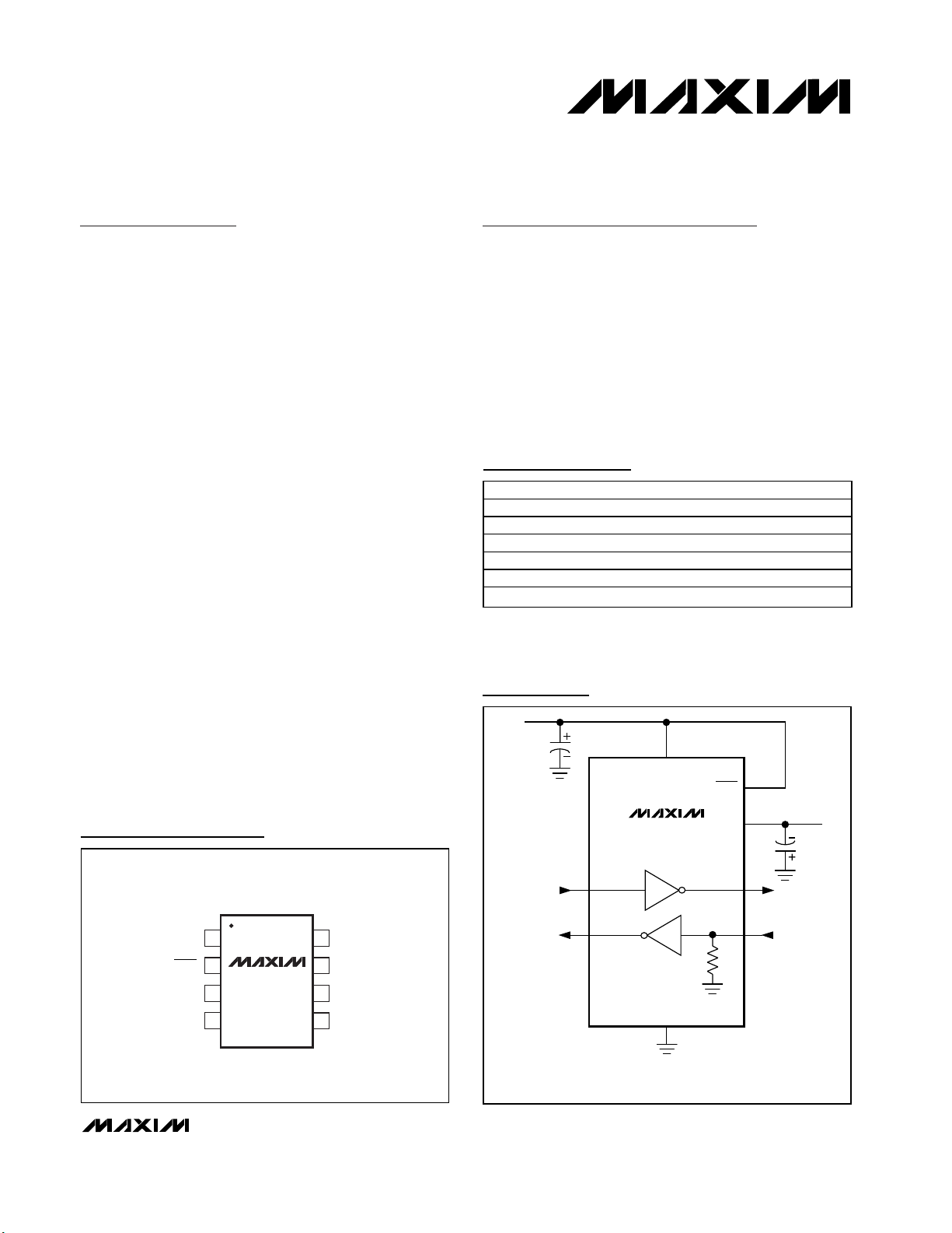
Pin Configuration
C
BYPASS
0.1µF
2
7
1
8
5
5kΩ
6
4
3
SHDN
V-
TOUT
RIN
TIN
ROUT
V
CC
GND
+5V
MAX3314
CAPACITORS MAY BE POLARIZED OR UNPOLARIZED.
-5V
0.1µF
Typical Operating Circuit
19-1725; Rev 1a; 3/01
Ordering Information
For pricing, delivery, and ordering information, please contact Maxim/Dallas Direct! at
1-888-629-4642, or visit Maxim’s website at www.maxim-ic.com.
PART TEMP. RANGE PIN-PACKAGE
MAX3314CKA 0°C to +70°C 8 SOT23
MAX3314CUA 0°C to +70°C 8 µMAX
MAX3314CSA 0°C to +70°C 8 SO
MAX3314EKA -40°C to +85°C 8 SOT23
MAX3314EUA -40°C to +85°C 8 µMAX
MAX3314ESA -40°C to +85°C 8 SO
TOP VIEW
1
V
CC
2
3
ROUT
4
SOT23/µMAX/SO
MAX3314
87GND
6
5
V-SHDN
RIN
TOUTTIN
Page 2
MAX3314
460kbps, 1µA, RS-232-Compatible Transceiver
2 _______________________________________________________________________________________
ABSOLUTE MAXIMUM RATINGS
ELECTRICAL CHARACTERISTICS
(VCC= +5V, V- = -5V, TA= T
MIN
to T
MAX
, unless otherwise noted. Typical values are at TA= +25°C.)
Stresses beyond those listed under “Absolute Maximum Ratings” may cause permanent damage to the device. These are stress ratings only, and functional
operation of the device at these or any other conditions beyond those indicated in the operational sections of the specifications is not implied. Exposure to
absolute maximum rating conditions for extended periods may affect device reliability.
Note 1: Not tested—guaranteed by design.
V
CC
to GND..............................................................-0.3V to +6V
V- to GND .................................................................+0.3V to -6V
Input Voltages
TIN, SHDN to GND ..............................................-0.3V to +6V
RIN to GND .....................................................................±25V
Output Voltages
TOUT to GND...............................................................±13.2V
ROUT .................................................…-0.3V to (V
CC
+ 0.3V)
Short-Circuit Duration
TOUT to GND ........................................................Continuous
Continuous Power Dissipation
8-Pin SOT23 (derate 9.7mW/°C above +70°C)...........777mW
8-Pin µMAX (derate 4.1mW/°C above +70°C) ............300mW
8-Pin SO (derate 5.88mW/°C above +70°C)...............471mW
Operating Temperature Ranges
MAX3314C_A.....................................................0°C to +70°C
MAX3314E_A..................................................-40°C to +85°C
Junction Temperature.....................................................+150°C
Storage Temperature Range ............................-65°C to +150°C
Lead Temperature (soldering, 10s) ................................+300°C
PARAMETER SYMBOL CONDITIONS MIN TYP MAX UNITS
DC CHARACTERISTICS
Positive Supply Operating
Range
Negative Supply Operating
Range
Positive Supply Current SHDN = V
Negative Supply Current SHDN = V
V
CC
4.75 5 5.25 V
V- -4.75 -5 -5.25 V
CC
CC
Shutdown Supply Current SHDN = GND 1 10 µA
LOGIC INPUTS (TIN, SHDN)
Input Logic Threshold Low V
Input Logic Threshold High V
IL
IH
0.8 V
2.4 V
Transmitter Input Hysteresis 0.5 V
Input Leakage Current ±0.01 µA
RECEIVER OUTPUT
Output Voltage Low V
Output Voltage High V
OL
OH
I
= 1.6mA 0.4 V
OUT
I
= -1.0mA
OUT
RECEIVER INPUT
Input Threshold Low V
Input Threshold High V
IL
IH
0.8 V
2.4 V
Input Hysteresis 0.5 V
Input Resistance 5 kΩ
TRANSMITTER OUTPUT
Transmitter output loaded with 3kΩ to
Output Voltage Swing
Output Resistance (Note 1) V
ground
= V- = 0, transmitter output = ±2V 300 Ω
CC
Output Short-Circuit Current ±60 mA
Output Leakage Current V
= ±12V, transmitter disabled
OUT
, no load 30 100 µA
, no load 15 30 µA
V
CC
- 0.3
V
CC
- 0.1
V
±3.7 V
25
µA
Page 3

MAX3314
460kbps, 1µA, RS-232-Compatible Transceiver
_______________________________________________________________________________________ 3
TIMING CHARACTERISTICS
(VCC= +5V, V- = -5V, TA= T
MIN
to T
MAX
, unless otherwise noted. Typical values are at TA= +25°C.)
Typical Operating Characteristics
(VCC= +5V, V- = -5V, 250kbps data rate, transmitter loaded with 3kΩ and CL, TA = +25°C, unless otherwise noted.)
0
2
1
5
4
3
8
7
6
9
0 1000500 1500 2000 2500 3000
SLEW RATE vs. LOAD CAPACITANCE
MAX3314-01
LOAD CAPACITANCE (pF)
SLEW RATE (V/us)
SLEW+
SLEW-
-6
-3
-4
-5
1
-1
0
-2
5
3
4
2
6
0 1000500 1500 2000 2500 3000
TRANSMITTER OUTPUT VOLTAGE
vs. LOAD CAPACITANCE
MAX3314-02
LOAD CAPACITANCE (pF)
TRANSMITTER OUTPUT VOLTAGE (V)
20kbps/120kbps
460kbps/250kbps
460kbps/250kbps
20kbps/120kbps
0
1.5
1.0
0.5
3.0
2.5
2.0
5.0
4.0
4.5
3.5
5.5
0 1000500 1500 2000 2500 3000
SUPPLY CURRENT
vs. LOAD CAPACITANCE
MAX3314-03
LOAD CAPACITANCE (pF)
SUPPLY CURRENT (mA)
120kbps
20kbps
250kbps
460kbps
Pin Description
PARAMETER SYMBOL CONDITIONS MIN TYP MAX UNITS
Maximum Data Rate
Receiver Propagation Delay
Transmitter Skew
Receiver Skew
Transition Region Slew Rate
t
PLH
t
PHL
R
= 3kΩ, C
L
=1000pf, transmitter switching 460 kbps
L
Receiver input to receiver output,
C
= 150pF
L
Receiver input to receiver output,
C
= 150pF
L
RL = 3kΩ to 7kΩ, CL = 150pF to 1000pF,
measured from +3V to -3V or from -3V to +3V
0.15
0.15
100 ns
50 ns
8 V/µs
µs
PIN NAME FUNCTION
1VCC± 5% E xter nal P ow er S up p l y. D ecoup l e w i th a 0.1µF cap aci tor to g r ound .
2 SHDN Shutdown Active Low. 0 = OFF, 1 = ON.
3 ROUT TTL/CMOS Receiver Output
4 TIN TTL/CMOS Transmitter Input
5 TOUT RS-232-Compatible Transmitter Output
6 RIN RS-232-Compatible Receiver Input
7V-±5% E xter nal P ow er S up p l y. D ecoup l e w i th a 0.1µF cap aci tor to g r ound .
8 GND Ground
Page 4
Detailed Description
RS-232-Compatible Drivers
The transmitter is an inverting level translator that converts CMOS-logic levels to EIA/TIA-232-compatible levels. It guarantees data rates up to 460kbps with
worst-case loads of 3kΩ in parallel with 1000pF. When
SHDN is driven low, the transmitter is disabled and put
into 3-state mode. The transmitter input does not have a
pull-up resistor. Connect to ground if unused.
RS-232-Compatible Receivers
The MAX3314’s receiver converts RS-232 signals to
CMOS-logic output levels. The receiver is rated to signals up to ±25V. The MAX3314’s receiver will remain
active during shutdown mode.
MAX3314 Shutdown Mode
In shutdown mode, the transmitter output is put into
high impedance. This reduces the supply current to
1µA. The time required to exit shutdown is less than
2.5µs. Table 1 is the shutdown logic truth table.
Applications Information
Capacitor Selection
The capacitor type used is not critical for proper operation; either polarized or nonpolarized capacitors are
acceptable. If polarized capacitors are used, connect
polarity as shown in the Typical Operating Circuit.
Bypass VCCand V- to ground with at least 0.1µF.
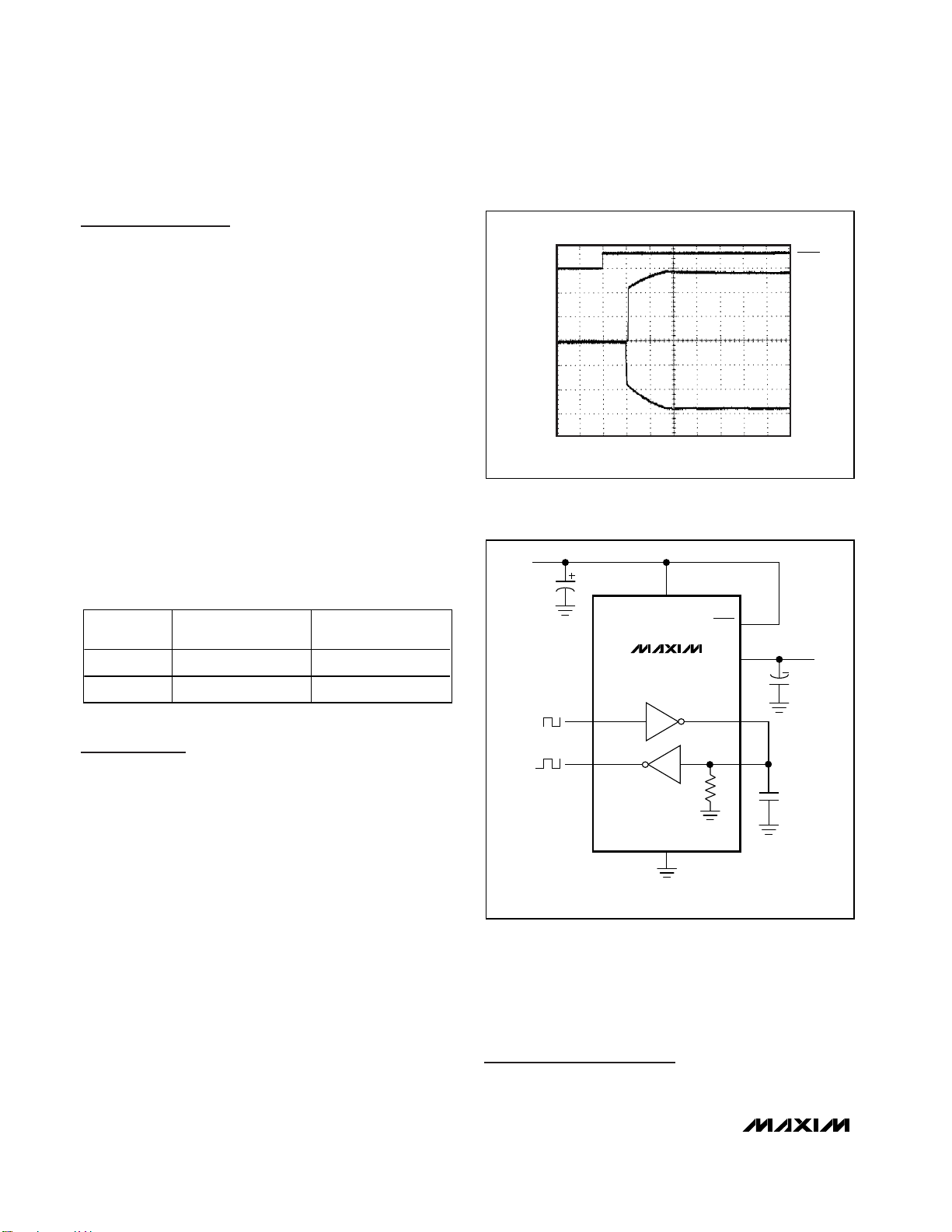
Transmitter Output When
Exiting Shutdown
Figure 1 shows the transmitter output when exiting shutdown mode. The transmitter is loaded with 3kΩ in parallel with 1000pF. The transmitter output displays no
ringing or undesirable transients as the MAX3314
comes out of shutdown. Note that the transmitter is
enabled only when the magnitude of V- exceeds
approximately -3V.
High Data Rates
The MAX3314 maintains minimum RS-232-compatible
±3.7V transmitter output voltage even at high data rates.
Figure 2 shows a transmitter loopback test circuit.
Figure 3 shows the loopback test result at 120kbps, and
Figure 4 shows the same test at 250kbps.
Chip Information
TRANSISTOR COUNT: 128
MAX3314
460kbps, 1µA, RS-232-Compatible Transceiver
4 _______________________________________________________________________________________
Table 1. Shutdown Logic Truth Table
Figure 1. Transmitter Output When Exiting Shutdown or
Powering Up
Figure 2. Loopback Test Circuit
5V/div
1.5V/div
0
0
1µs/div
TIN = GND
TIN = V
CC
SHDN
TOUT
SHDN
L High-Z Active
H Active Active
TRANSMITTER
OUTPUT
RECEIVER
OUTPUT
+5V
0.1µF
V
CC
SHDN
MAX3314
TIN
ROUT
GND
CAPACITORS MAY BE POLARIZED OR NONPOLARIZED.
V-
TOUT
RIN
5kΩ
-5V
0.1µF
1000pF
Page 5

MAX3314
460kbps, 1µA, RS-232-Compatible Transceiver
_______________________________________________________________________________________ 5
Figure 4. Loopback Test Results at 250kbps
Figure 3. Loopback Test Results at 120kbps
Package InformationPackage Information
5µs/div
TIN
TOUT
ROUT
TIN
TOUT
ROUT
2µs/div
Page 6

MAX3314
460kbps, 1µA, RS-232-Compatible Transceiver
Maxim cannot assume responsibility for use of any circuitry other than circuitry entirely embodied in a Maxim product. No circuit patent licenses are
implied. Maxim reserves the right to change the circuitry and specifications without notice at any time.
6 _____________________Maxim Integrated Products, 120 San Gabriel Drive, Sunnyvale, CA 94086 408-737-7600
© 2001 Maxim Integrated Products Printed USA is a registered trademark of Maxim Integrated Products.
Package Information (continued)
SOICN.EPS
SOT23, 8L.EPS
 Loading...