

General Description
The MAX3311E/MAX3313E are low-power, 5V EIA/TIA232-compatible transceivers. All transmitter outputs
and receiver inputs are protected to ±15kV using the
Human Body Model, making these devices ideal for
applications where more robust transceivers are
required.
Both devices have one transmitter and one receiver.
The transmitters have a proprietary low-dropout transmitter output stage enabling RS-232-compatible operation from a +5V supply with a single inverting charge
pump. These transceivers require only three 0.1µF
capacitors and will run at data rates up to 460kbps
while maintaining RS-232-compatible output levels.
The MAX3311E features a 1µA shutdown mode. In
shutdown the device turns off the charge pump, pulls
V- to ground, and the transmitter output is disabled.
The MAX3313E features an INVALID output that asserts
high when an active RS-232 cable signal is connected,
signaling to the host that a peripheral is connected to
the communication port.
________________________Applications
Digital Cameras
PDAs
GPS
POS
Telecommunications
Handy Terminals
Set-Top Boxes
Features
♦ ESD Protection for RS-232-Compatible I/O Pins
±15kV—Human Body Model
♦ 1µA Low-Power Shutdown (MAX3311E)
♦ INVALID Output (MAX3313E)
♦ Receiver Active in Shutdown (MAX3311E)
♦ Single Transceiver (1Tx/1Rx) in 10-Pin µMAX
Package
MAX3311E/MAX3313E
±15kV ESD-Protected, 460kbps, 1µA,
RS-232-Compatible Transceivers in µMAX
________________________________________________________________ Maxim Integrated Products 1
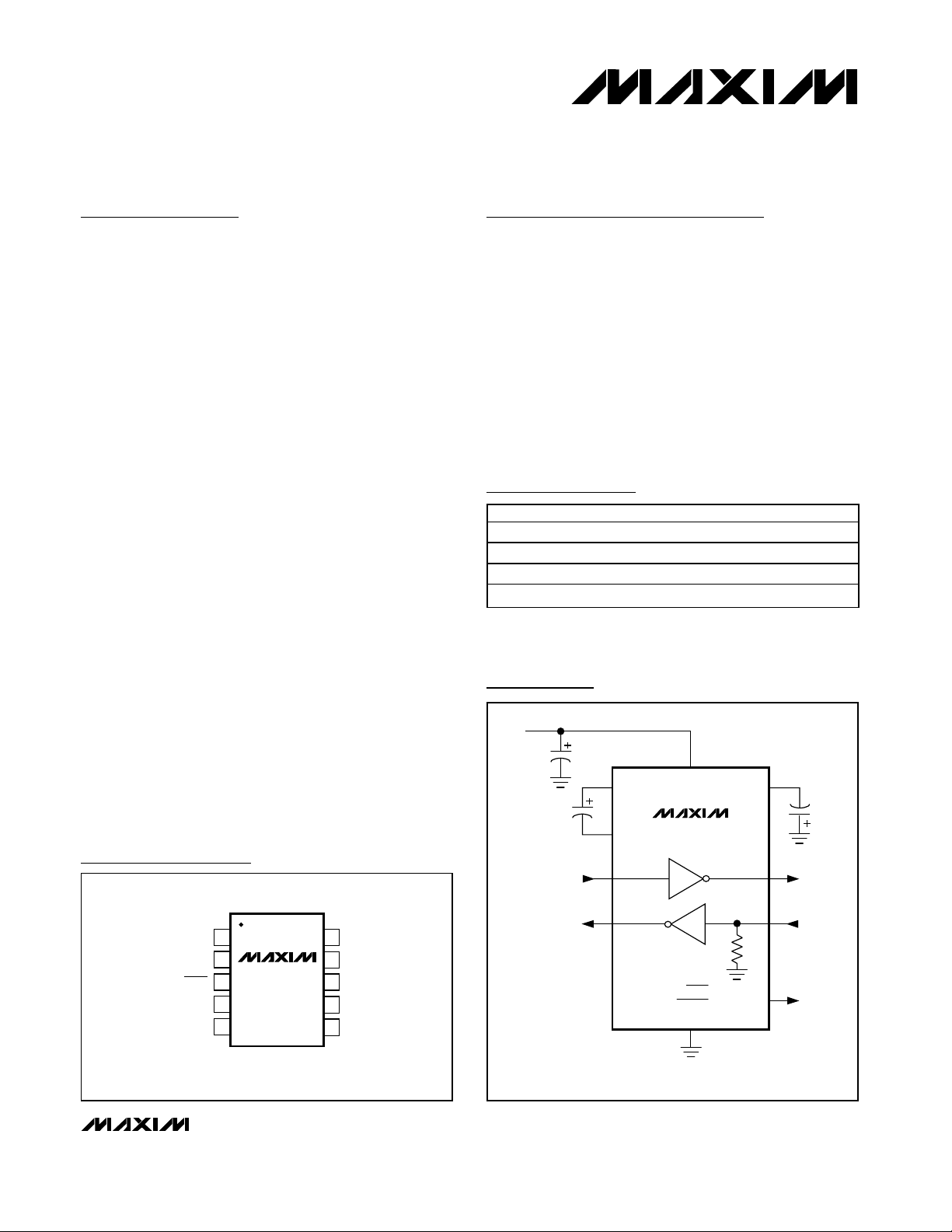
Pin Configurations
19-1910; Rev 0; 1/01
Ordering Information
1
2
3
4
5
10
9
8
7
6
GND
C1+
VTOUTTIN
SHDN
C1-
V
CC
MAX3311E
µMAX
TOP VIEW
RINROUT
For price, delivery, and to place orders, please contact Maxim Distribution at 1-888-629-4642,
or visit Maxim’s website at www.maxim-ic.com.
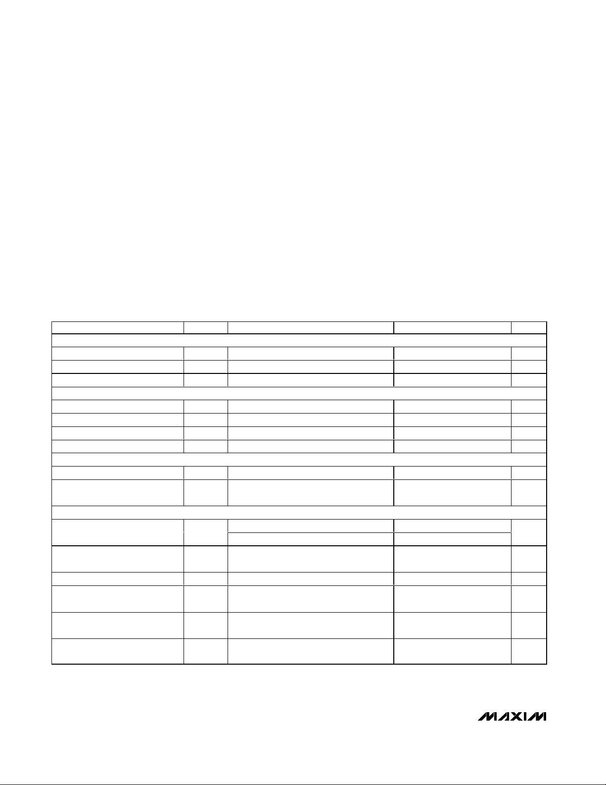
C1
0.1µF
C2
0.1µF
C
BYPASS
0.1µF
98
1
10
7
6
3
2
4
5
C1+ V-
TOUT
RIN
C1-
TIN
ROUT
V
CC
GND
5k
SHDN (MAX3311E)
INVALID (MAX3313E)
+5V
MAX3311E
MAX3313E
CAPACITORS MAY BE POLARIZED OR NONPOLARIZED.
Typical Operating Circuit
Pin Configurations continued at end of data sheet.
PART
TEMP. RANGE
PIN-PACKAGE
MAX3311ECUB 0°C to +70°C 10 µMAX
MAX3311EEUB -40°C to +85°C 10 µMAX
MAX3313ECUB 0°C to +70°C 10 µMAX
MAX3313EEUB -40°C to +85°C 10 µMAX
MAX3311E/MAX3313E
±15kV ESD-Protected, 460kbps, 1µA,
RS-232-Compatible Transceivers in µMAX
2 _______________________________________________________________________________________
ABSOLUTE MAXIMUM RATINGS
ELECTRICAL CHARACTERISTICS
(VCC= +5V, C1 and C2 = 0.1µF, TA= T
MIN
to T
MAX
. Typical values are at TA= +25°C.)
Stresses beyond those listed under “Absolute Maximum Ratings” may cause permanent damage to the device. These are stress ratings only, and functional
operation of the device at these or any other conditions beyond those indicated in the operational sections of the specifications is not implied. Exposure to
absolute maximum rating conditions for extended periods may affect device reliability.
VCCto GND.............................................................-0.3V to +6V
V- to GND................................................................+0.3V to -7V
V
CC
+ |V-|............................................................................+13V
Input Voltages
TIN, SHDN to GND...............................................-0.3V to +6V
RIN to GND......................................................................±25V
Output Voltages
TOUT to GND................................................................±13.2V
ROUT, INVALID to GND.....................…-0.3V to (V
CC
+ 0.3V)
Short-Circuit Duration
TOUT to GND.........................................................Continuous
Continuous Power Dissipation
10-Pin µMAX (derate 5.6mW/°C above +70°C)..........444mW
Operating Temperature Ranges
MAX331_ECUB.................................................0°C to +70°C
MAX331_EEUB..............................................-40°C to +85°C
Junction Temperature.....................................................+150°C
Storage Temperature Range............................-65°C to +150°C
Lead Temperature (soldering, 10s)................................+300°C
PARAMETER
SYMBOL
CONDITIONS MIN TYP
MAX
UNITS
DC CHARACTERISTICS
Supply Operation Range V
CC
4.5 5 5.5 V
Supply Current SHDN = V
CC
, no load 100 250 µA
Shutdown Supply Current SHDN = GND (MAX3311E only) 1
µA
LOGIC INPUTS (TIN, SHDN)
Input Logic Threshold Low V
IL
0.8 V
Input Logic Threshold High V
IH
2.4 V
Transmitter Input Hysteresis 0.5 V
Input Leakage Current
±1 µA
RECEIVER OUTPUT
Output Voltage Low V
OL
I
OUT
= 1.6mA 0.4 V
Output Voltage High V
OH
I
OUT
= -1.0mA
V
INVALID OUTPUT (MAX3313E only)
Figure 7, positive threshold 2.7
Receiver Input Threshold to
INVALID Output High
Figure 7, negative threshold -2.7
V
Receiver Input Threshold to
INVALID Output Low
Figure 7 -0.3 0.3
V
INVALID Output Low V
OL
I
OUT
= 1.6mA 0.4 V
INVALID Output High V
OH
I
OUT
= -1.0mA
V
Receiver Positive or Negative
Thresholds to INVALID High
Figure 7 0.1 µs
Receiver Positive or Negative
Threshold to INVALID Low
Figure 7 30 µs
10
±0.01
V
CC
- 0.6 V
CC
- 0.1
V
CC
- 0.6
MAX3311E/MAX3313E
±15kV ESD-Protected, 460kbps, 1µA,
RS-232-Compatible Transceivers in µMAX
_______________________________________________________________________________________ 3
ELECTRICAL CHARACTERISTICS (continued)
(VCC= +5V, C1 and C2 = 0.1µF, TA= T
MIN
to T
MAX
. Typical values are at TA= +25°C.)
TIMING CHARACTERISTICS
(VCC= +5V, C1 and C2 = 0.1µF, TA= T
MIN
to T
MAX
. Typical values are at TA= +25°C.)
PARAMETER
SYMBOL
CONDITIONS MIN TYP
MAX
UNITS
RECEIVER INPUT
Input Threshold Low V
IL
0.8 V
Input Threshold High V
IH
2.4 V
Input Hysteresis 0.5 V
Input Resistance 5 kΩ
TRANSMITTER OUTPUT
Output Voltage Swing
Tr ansm i tter outp ut l oad ed w i th 3kΩ to
±3.7 V
Output Resistance (Note 1) V
CC
= 0, transmitter output = ±2V 300 Ω
Output Short-Circuit Current ±60 mA
Output Leakage Current V
OUT
= ±12V, transmitter disabled
±25 µA
ESD PERFORMANCE (TRANSMITTER OUTPUT, RECEIVER INPUT)
ESD-Protection Voltage Human Body Model ±15 kV
Note 1: Not tested—guaranteed by design.
PARAMETER SYMBOL CONDITIONS MIN TYP MAX UNITS
Maximum Data Rate R
Receiver Propagation Delay t
PLH/tPHL
= 3kΩ, C
L
= 1000pF 460 kbps
L
Receiver input to receiver output,
= 150pF
C
L
0.15 µs
Transmitter Skew 100 ns
Receiver Skew 50 ns
RL = 3kΩ to 7kΩ, CL = 150pF to 1000pF,
Transition Region Slew Rate
measured from +3V to -3V or from -3V to +3V
11
V/µs

MAX3311E/MAX3313E
±15kV ESD-Protected, 460kbps, 1µA,
RS-232-Compatible Transceivers in µMAX
4 _______________________________________________________________________________________
Typical Operating Characteristics
(VCC= +5V, 0.1µF capacitors, transmitter loaded with 3kΩ and CL, TA= +25°C, unless otherwise noted.)
0
4
2
8
6
12
10
14
0 1000 1500500 2000 2500 3000
SLEW RATE
vs. LOAD CAPACITANCE
MAX3311E/13E-01
LOAD CAPACITANCE (pF)
SLEW RATE (V/µs)
+SLEW
250 kbps DATA RATE
-SLEW
-5
-4
-3
-2
-1
0
1
2
3
4
5
6
0 500 1000 1500 2000 2500 3000
TRANSMITTER OUTPUT VOLTAGE
vs. LOAD CAPACITANCE
MAX3311E/13E-02
LOAD CAPACITANCE (pF)
TRANSMITTER OUTPUT VOLTAGE (V)
460kbps/250kbps/120kbps
460kbps/250kbps/120kbps
0
4
2
8
6
12
10
14
0 1000 1500500 2000 2500 3000
SUPPLY CURRENT
vs. LOAD CAPACITANCE
MAX3311E/13E-03
LOAD CAPACITANCE (pF)
SUPPLY CURRENT (mA)
20kbps
120kbps
250kbps
460kbps
Pin Description
PIN
MAX3311E MAX3313E
NAME FUNCTION
11V
CC
+5V External Power Supply. Decouple with a 0.1µF capacitor to ground.
2 2 C1- Negative Terminal of the Voltage Inverter Charge-Pump Capacitor
3 — SHDN Shutdown Active Low (0 = off, 1 = on)
— 3 INVALID
Valid Signal Detector Output, Active Low. A logic high indicates that a valid
RS-232 level is present on the receiver input.
4 4 TIN TTL/CMOS Transmitter input
5 5 ROUT TTL/CMOS Receiver output
6 6 RIN ±15kV ESD-Protected, RS-232 Receiver Input
7 7 TOUT ±15kV ESD-Protected, RS-232-Compatible Transmitter Output
8 8 V- -4.3V generated by the charge pump. Connect a 0.1µF capacitor to ground.
9 9 C1+ Positive Terminal of the Voltage Inverter Charge-Pump Capacitor
10 10 GND Ground

Detailed Description
Single Charge-Pump Voltage Converter
The MAX3311E/MAX3313E internal power supply has a
single inverting charge pump that provides a negative
voltage from a single +5V supply. The charge pump
operates in a discontinuous mode and requires a flying
capacitor (C1) and a reservoir capacitor (C2) to generate the V- supply.
RS-232-Compatible Driver
The transmitter is an inverting level translator that converts CMOS-logic levels to EIA/TIA-232 compatible levels. It guarantees data rates up to 460kbps with
worst-case loads of 3kΩ in parallel with 1000pF. When
SHDN is driven low, the transmitter is disabled and put
into tri-state. The transmitter input does not have an
internal pullup resistor.
RS-232 Receiver
The MAX3311E/MAX3313E receiver converts RS-232
signals to CMOS-logic output levels. The MAX3311E
receiver will remain active during shutdown mode. The
MAX3313E INVALID indicates when an RS-232 signal
is present at the receiver input, and therefore when the
port is in use.
The MAX3313E INVALID output is pulled low when no
valid RS-232 signal level is detected on the receiver
input.
MAX3311E Shutdown Mode
In shutdown mode, the charge pump is turned off, V- is
pulled to ground, and the transmitter output is disabled
(Table 1). This reduces supply current typically to 1µA.
The time required to exit shutdown is less than 25ms.
Applications Information
Capacitor Selection
The capacitor type used for C1 and C2 is not critical for
proper operation; either polarized or nonpolarized
capacitors are acceptable. If polarized capacitors are
used, connect polarity as shown in the Typical
Operating Circuit. The charge pump requires 0.1µF
capacitors. Increasing the capacitor values (e.g., by a
factor of 2) reduces power consumption. C2 can be
increased without changing C1’s value. However, do
not increase C1’s value without also increasing the
value of C2 and C
BYPASS
to maintain the proper ratios
(C1 to the other capacitors).
When using the minimum 0.1µF capacitors, make sure
the capacitance does not degrade excessively with
temperature. If in doubt, use capacitors with a larger
nominal value. The capacitor’s equivalent series resistance (ESR) usually rises at low temperatures and influences the amount of ripple on V-.
To reduce the output impedance at V-, use larger
capacitors (up to 10µF).
Bypass VCCto ground with at least 0.1µF. In applications sensitive to power-supply noise generated by the
charge pump, decouple VCCto ground with a capacitor the same size as (or larger than) charge-pump
capacitors C1 and C2.
Transmitter Output when Exiting
Shutdown
Figure 1 shows the transmitter output when exiting
shutdown mode. The transmitter is loaded with 3kΩ in
parallel with 1000pF. The transmitter output displays no
ringing or undesirable transients as the MAX3311E
comes out of shutdown. Note that the transmitter is
enabled only when the magnitude of V- exceeds
approximately -3V.
High Data Rates
The MAX3311E/MAX3313E maintain RS-232-compatible ±3.7V minimum transmitter output voltage even at
MAX3311E/MAX3313E
±15kV ESD-Protected, 460kbps, 1µA,
RS-232-Compatible Transceivers in µMAX
_______________________________________________________________________________________ 5
Table 1. MAX3311E Shutdown Logic
Truth Table
SHDN
TRANSMITTER
OUTPUT
RECEIVER
OUTPUT
CHARGE
PUMP
L High Z Active Inactive
H Active Active Active
Figure 1. Transmitter Output when Exiting Shutdown or
Powering Up
10µs/div
SHDN
TOUT
5V/div
0
1.5V/div
0
TIN = GND
TIN = V
CC

MAX3311E/MAX3313E
±15kV ESD-Protected, 460kbps, 1µA,
RS-232-Compatible Transceivers in µMAX
6 _______________________________________________________________________________________
high data rates. Figure 2 shows a transmitter loopback
test circuit. Figure 3 shows the loopback test result at
120kbps, and Figure 4 shows the same test at
250kbps.
±15kV ESD Protection
As with all Maxim devices, ESD-protection structures
are incorporated on all pins to protect against electrostatic discharges encountered during handling and
assembly. The MAX3311E/MAX3313E driver outputs
and receiver inputs have extra protection against static
discharge. Maxim’s engineers have developed state-ofthe-art structures to protect these pins against ESD of
±15kV without damage. The ESD structures withstand
high ESD in all states: normal operation, shutdown, and
powered down. After an ESD event, Maxim’s E versions
keep working without latchup; whereas, competing
products can latch and must be powered down to
remove latchup.
ESD protection can be tested in various ways. The
transmitter outputs and receiver inputs of the product
family are characterized for protection to ±15kV using
the Human Body Model.
ESD Test Conditions
ESD performance depends on a variety of conditions.
Contact Maxim for a reliability report that documents
test setup, test methodology, and test results.
Human Body Model
Figure 5 shows the Human Body Model, and Figure 6
shows the current waveform it generates when discharged into low impedance. This model consists of a
100pF capacitor charged to the ESD voltage of interest,
which is then discharged into the test device through a
1.5kΩ resistor.
Machine Model
The Machine Model for ESD tests all pins using a
200pF storage capacitor and zero discharge resistance. Its objective is to emulate the stress caused by
contact that occurs with handling and assembly during
manufacturing. Of course, all pins require this protection during manufacturing, not just RS-232 inputs and
outputs. Therefore, after PC board assembly, the
Machine Model is less relevant to I/O ports.
Figure 2. Loopback Test Circuit
C1
C2
0.1µF
V-
TOUT
TIN
ROUT
1000pF
RIN
V
CC
GND
5k
+5V
MAX3311E
MAX3313E
C1+
C1-
Figure 4. Loopback Test Results at 250kbps
2µs/div
TOUT
TIN
ROUT
Figure 3. Loopback Test Results at 120kbps
5µs/div
TOUT
TIN
ROUT

MAX3311E/MAX3313E
±15kV ESD-Protected, 460kbps, 1µA,
RS-232-Compatible Transceivers in µMAX
_______________________________________________________________________________________ 7
Figure 5. Human Body ESD Test Model
CHARGE-CURRENT
LIMIT RESISTOR
DISCHARGE
RESISTANCE
STORAGE
CAPACITOR
C
s
100pF
R
C
1MΩ
R
D
1500Ω
HIGH-
VOLTAGE
DC
SOURCE
DEVICE
UNDER
TEST
Figure 6. Human Body Current Waveform
IP 100%
90%
36.8%
t
RL
TIME
t
DL
CURRENT WAVEFORM
PEAK-TO-PEAK RINGING
(NOT DRAWN TO SCALE)
I
r
10%
0
0
AMPERES
Figure 7. Receiver Positive/Negative Thresholds for
INVALID
RECEIVER INPUT LEVELS
-2.7V
-0.3V
+2.7V
+0.3V
0
INDETERMINATE
INVALID HIGH
INVALID LOW
INVALID HIGH
INDETERMINATE
Pin Configurations (continued)
Chip Information
TRANSISTOR COUNT: 278
V
C1-
INVALID
1
CC
2
MAX3313E
3
4
5
MAX
µ
10
9
8
7
6
GND
C1+
VTOUTTIN
RINROUT

MAX3311E/MAX3313E
±15kV ESD-Protected, 460kbps, 1µA,
RS-232-Compatible Transceivers in µMAX
Maxim cannot assume responsibility for use of any circuitry other than circuitry entirely embodied in a Maxim product. No circuit patent licenses are
implied. Maxim reserves the right to change the circuitry and specifications without notice at any time.
8 _____________________Maxim Integrated Products, 120 San Gabriel Drive, Sunnyvale, CA 94086 408-737-7600
© 2001 Maxim Integrated Products Printed USA is a registered trademark of Maxim Integrated Products.
10LUMAX.EPS
______________________________________________________________Pin Description
 Loading...