

Page 1
General Description
The MAX3301E/MAX3302E fully integrated USB On-theGo (OTG) transceivers and charge pumps allow mobile
devices such as PDAs, cellular phones, and digital
cameras to interface directly with USB peripherals and
each other without the need of a host PC. Use the
MAX3301E/MAX3302E with an embedded USB host to
directly connect to peripherals such as printers or
external hard drives.
The MAX3301E/MAX3302E integrate a USB OTG transceiver, a V
BUS
charge pump, a linear regulator, and an
I
2
C-compatible, 2-wire serial interface. An internal level
shifter allows the MAX3301E/MAX3302E to interface
with +1.65V to +3.6V logic supply voltages. The
MAX3301E/MAX3302E’s OTG-compliant charge pump
operates with +3V to +4.5V input supply voltages, and
supplies an OTG-compatible output on V
BUS
while
sourcing more than 8mA of output current.
The MAX3301E/MAX3302E enable USB OTG communi-
cation from highly integrated digital devices that cannot
supply or tolerate the +5V V
BUS
levels that USB OTG
requires. The device supports USB OTG session-request
protocol (SRP) and host-negotiation protocol (HNP).
The MAX3301E/MAX3302E provide built-in ±15kV electrostatic-discharge (ESD) protection for the V
BUS
, ID_IN,
D+, and D- terminals. The MAX3301E/MAX3302E are
available in 25-bump chip-scale (UCSP™), 25-bump
WLP package, 28-pin TQFN, and 32-pin TQFN packages and operate over the extended -40°C to +85°C
temperature range.
Applications
Mobile Phones Digital Cameras
PDAs MP3 Players
Features
o USB 2.0-Compliant Full-/Low-Speed OTG
Transceivers
o Ideal for USB On-the-Go, Embedded Host, or
Peripheral Devices
o ±15kV ESD Protection on ID_IN, V
BUS
, D+, and D-
Terminals
o Charge Pump for V
BUS
Signaling and Operation
Down to 3V
o Internal V
BUS
and ID Comparators
o Internal Switchable Pullup and Pulldown
Resistors for Host/Peripheral Functionality
o I
2
C Bus Interface with Command and Status
Registers
o Linear Regulator Powers Internal Circuitry and
D+/D- Pullup Resistors
o Support SRP and HNP
MAX3301E/MAX3302E
USB On-the-Go Transceivers and Charge Pumps
________________________________________________________________
Maxim Integrated Products
1
Ordering Information
19-3275; Rev 3; 10/07
For pricing, delivery, and ordering information, please contact Maxim Direct at 1-888-629-4642,
or visit Maxim’s website at www.maxim-ic.com.
Note: All devices specified over the -40°C to +85°C operating
range.
‡
UCSP bumps are in a 5 x 5 array. The UCSP package size is
2.5mm x 2.5mm x 0.62mm. Requires solder temperature profile
described in the Absolute Maximum Ratings section. UCSP reliability is integrally linked to the user’s assembly methods, circuit
board material and environment. See the UCSP Applications
Information section of this data sheet for more information.
*
Future product—contact factory for availability.
**
EP = Exposed paddle.
T = Tape and reel.
+
Denotes a lead-free package.
Selector Guide
†
The MAX3301E powers up in its lowest power state and the
MAX3302E powers up in the operational, VP/VM USB mode.
Pin Configurations appear at end of data sheet.
I2C ADDRESSES FOR
†
PART POWER-UP STATE
Shutdown (sdwn = 1,
MAX3301E
MAX3302E
bit 0 of specialfunction register 2)
Operating (sdwn = 1,
bit 0 of specialfunction register 2)
SPECIAL-FUNCTION
REGISTER 2
16h, 17h
10h, 11h, and 16h, 17h
PACKAGE
PART
MAX3301EEBA-T 2.5 x 2.5 25 UCSP
MAX3301EETJ 5 x 5 32 TQFN-EP** T3255-4
MAX3302EEBA-T* 2.5 x 2.5 25 UCSP
MAX3302EETI 4 x 4 28 TQFN-EP** T2844-1
MAX3302EEWA+T 2.54 x 2.54 25 WLP W252A2-1
SIZE
(mm)
PINPACKAGE
‡
‡
PKG
CODE
B25-1
B25-1
Page 2
MAX3301E/MAX3302E
USB On-the-Go Transceivers and Charge Pumps
2 _______________________________________________________________________________________
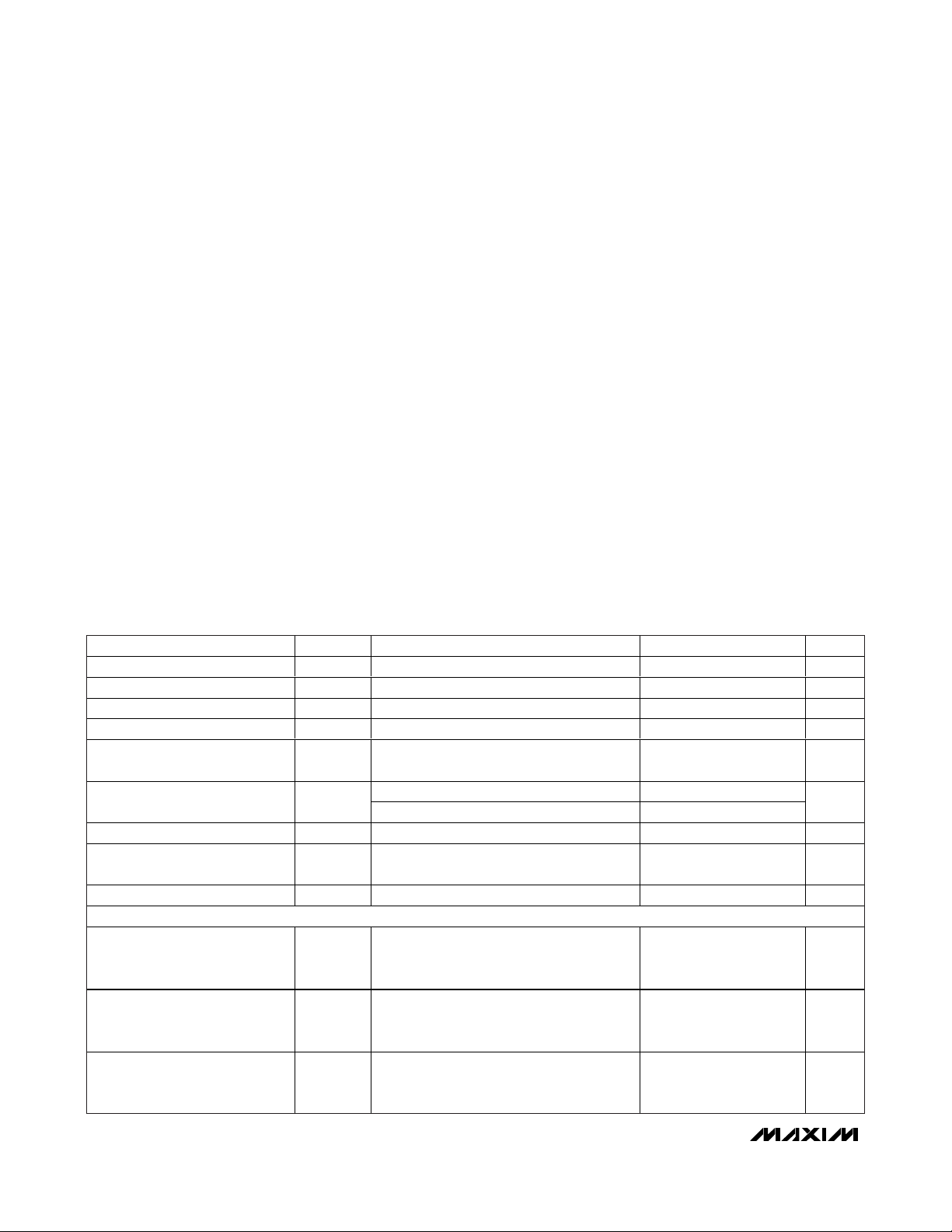
ABSOLUTE MAXIMUM RATINGS
DC ELECTRICAL CHARACTERISTICS
(VCC= +3V to +4.5V, VL= +1.65V to +3.6V, C
FLYING
= 100nF, C
VBUS
= 1µF, ESR
CVBUS
= 0.1Ω (max), TA= T
MIN
to T
MAX
, unless
otherwise noted. Typical values are at V
CC
= +3.7V, VL= +2.5V, TA= +25°C.) (Note 2)
Note 1: The UCSP package is constructed using a unique set of packaging techniques that impose a limit on the thermal profile the
device can be exposed to during board-level solder attach and rework. This limit permits only the use of the solder profiles recommended in the industry-standard specification, JEDEC 020A, paragraph 7.6, Table 3 for IR/VPR and convection reflow. Preheating is
required. Hand or wave soldering is not allowed.
Stresses beyond those listed under “Absolute Maximum Ratings” may cause permanent damage to the device. These are stress ratings only, and functional
operation of the device at these or any other conditions beyond those indicated in the operational sections of the specifications is not implied. Exposure to
absolute maximum rating conditions for extended periods may affect device reliability.
All voltages are referenced to GND.
V
CC
, VL.....................................................................-0.3V to +6V
TRM (regulator off or supplied by V
BUS
) ..-0.3V to (V
BUS
+ 0.3V)
TRM (regulator supplied by V
CC
)...............-0.3V to (VCC+ 0.3V)
D+, D- (transmitter tri-stated) ...................................-0.3V to +6V
D+, D- (transmitter functional)....................-0.3V to (V
CC
+ 0.3V)
V
BUS
.........................................................................-0.3V to +6V
ID_IN, SCL, SDA.......................................................-0.3V to +6V
INT, SPD, RESET, ADD, OE/INT, RCV, VP,
VM, SUS, DAT_VP, SE0_VM ......................-0.3V to (V
L
+ 0.3V)
C+.............................................................-0.3V to (V
BUS
+ 0.3V)
C-................................................................-0.3V to (V
CC
+ 0.3V)
Short-Circuit Duration, V
BUS
to GND .........................Continuous
Continuous Power Dissipation (T
A
= +70°C)
25-Bump WLP (derate 12.2mW/°C above +70°C).......976mW
25-Bump UCSP (derate 12.2mW/°C above +70°C) ....976mW
32-Pin TQFN (5mm x 5mm x 0.8mm) (derate 21.3mW/°C
above +70°C).........................................................1702mW
28-Pin TQFN (4mm x 4mm x 0.8mm) (derate 20.8mW/°C
above +70°C).........................................................1666mW
Operating Temperature Range ...........................-40°C to +85°C
Junction Temperature......................................................+150°C
Storage Temperature Range .............................-65°C to +150°C
Lead Temperature (soldering, 10s) .................................+300°C
Bump Reflow Temperature (Note 1)
Infrared (15s) ...............................................................+200°C
Vapor Phase (20s) .......................................................+215°C
)
)
PARAMETER SYM B O L CONDITIONS MIN TYP MAX UNITS
Supply Voltage V
TRM Output Voltage V
Logic Supply Voltage V
VL Supply Current I
VCC Operating Supply Current I
CC
TRM
L
VL
CC
VCC Supply Current During FullSpeed Idle
VCC Shutdown Supply Current I
VCC Interrupt Shutdown Supply
Current
CC(SHDN
I
CC(ISHDN
VCC Suspend Supply Current U SB suspend mode, ID _IN unconnected or hig h 170 500 µA
LOGIC I/O
RC V , D AT_V P , S E 0_V M , INT,
OE/INT, V P , V M Outp ut H i g h
V
OH
V ol tag e
3.0 4.5 V
3.0 3.6 V
1.65 3.60 V
I2C interface in steady state 5 µA
USB normal mode, CL = 50pF, device
switching at full speed
V
VBUS_DRV
V
VBUS_DRV
= 1, I
= 0 1.4 2
VBUS
= 0, D+ = high, D- = low 0.5 0.8
10 mA
3.5 10 µA
ID_IN unconnected or high 20 30 µA
I
= 1mA (sourcing) V L - 0.4 V
OUT
mA
RCV, DAT_VP, SE0_VM, INT,
OE/INT, VP, VM Output Low
V
OL
I
= 1mA (sinking) 0.4 V
OUT
Voltage
OE/INT, SPD, SUS, RESET,
DAT_VP, SE0_VM Input High
V
IH
2/3 x V
L
Voltage
V
Page 3
MAX3301E/MAX3302E
USB On-the-Go Transceivers and Charge Pumps
_______________________________________________________________________________________ 3
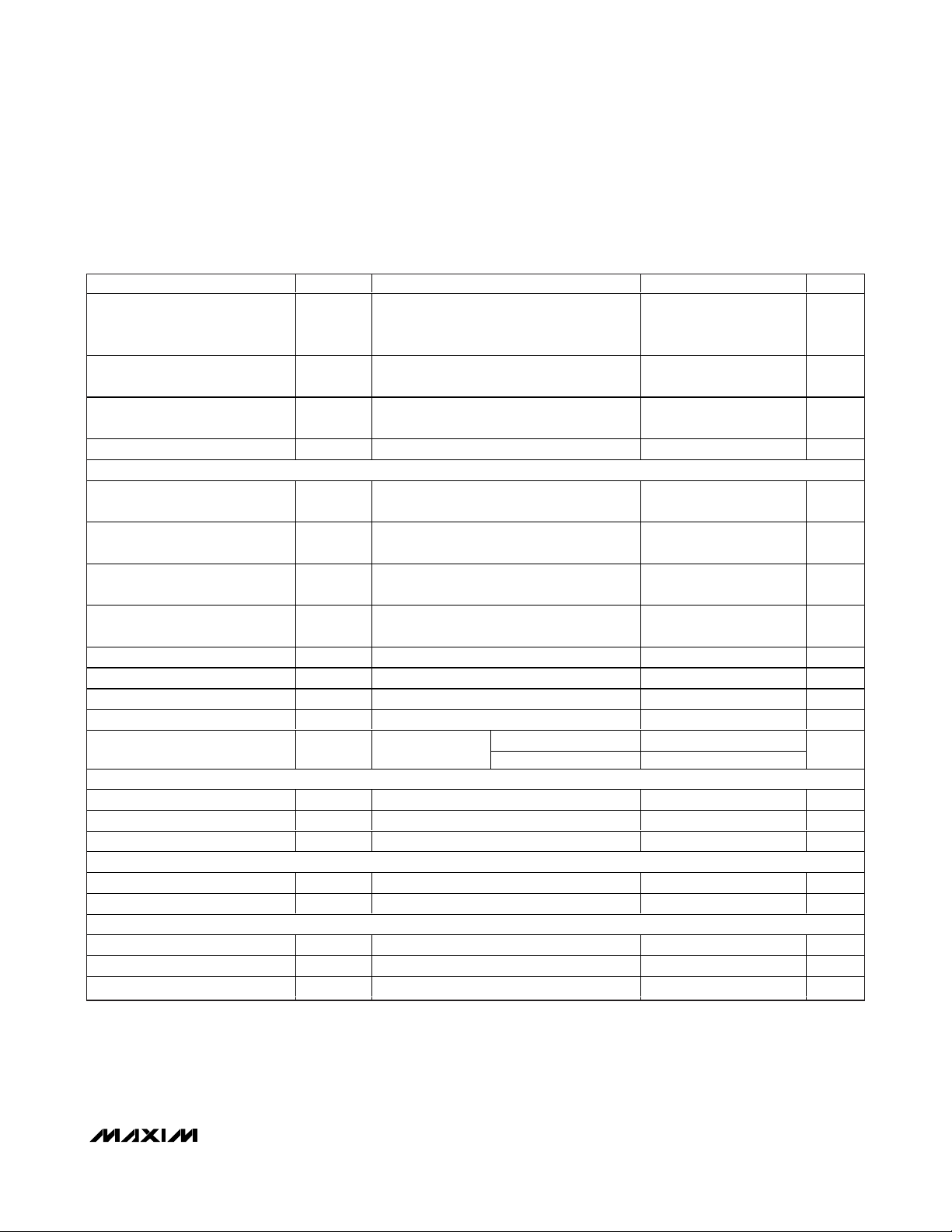
DC ELECTRICAL CHARACTERISTICS (continued)
(VCC= +3V to +4.5V, VL= +1.65V to +3.6V, C
FLYING
= 100nF, C
VBUS
= 1µF, ESR
CVBUS
= 0.1Ω (max), TA= T
MIN
to T
MAX
, unless
otherwise noted. Typical values are at V
CC
= +3.7V, VL= +2.5V, TA= +25°C.) (Note 2)
PARAMETER SYM B O L CONDITIONS MIN TYP MAX UNITS
OE/INT, SPD, SUS, RESET
DAT_VP, SE0_VM Input Low
V
IL
0.4 V
Voltage
ADD Input High Voltage V
ADD Input Low Voltage V
IHA
ILA
2/3 x V
L
1/3 x V
V
V
L
Input Leakage Current ±1µA
TRANSCEIVER SPECIFICATIONS
Differential Receiver Input
Sensitivity
Differential Receiver CommonMode Voltage
Single-Ended Receiver Input Low
Voltage
Single-Ended Receiver Input
High Voltage
V
ILD
V
IHD
- VD-| 0.2 V
|V
D+
0.8 2.5 V
D+, D- 0.8 V
D+, D- 2.0 V
S i ng l e- E nd ed Recei ver H yster esi s 0.2 V
S i ng l e- E nd ed Outp ut Low V ol tag eV
S i ng l e- E nd ed Outp ut H i g h V ol tag eV
OLD
OHD
D+, D-, RL = 1.5kΩ from D+ or D- to 3.6V 0.3 V
D+, D-, RL = 15kΩ from D+ or D- to GND 2.8 3.6 V
Off-State Leakage Current D+, D- ±1µA
Driver Output Impedance
ESD PROTECTION (V
BUS
, ID_IN, D+, D-)
D+, D-, not
including R
EXT High steady-state drive 2 13
Low steady-state drive 2 13
Ω
Human Body Model ±15 kV
IEC 61000-4-2 Air-Gap Discharge ±10 kV
IEC 61000-4-2 Contact Discharge ±6kV
THERMAL SHUTDOWN
Thermal Shutdown Low-to-High +160
Thermal Shutdown High-to-Low +150
o
C
o
C
CHARGE-PUMP SPECIFICATIONS (vbus_drv = 1)
V
Output Voltage V
BUS
V
Output Current I
BUS
V
Output Ripple I
BUS
BUS
VBUS
3V < V
VBUS
< 4.5V, C
C C
= 8mA, C
V BUS
= 10µF, I
= 8m A 4.80 5.25 V
V BUS
8mA
= 10µF 100 mV
VBUS
Page 4
MAX3301E/MAX3302E
USB On-the-Go Transceivers and Charge Pumps
4 _______________________________________________________________________________________
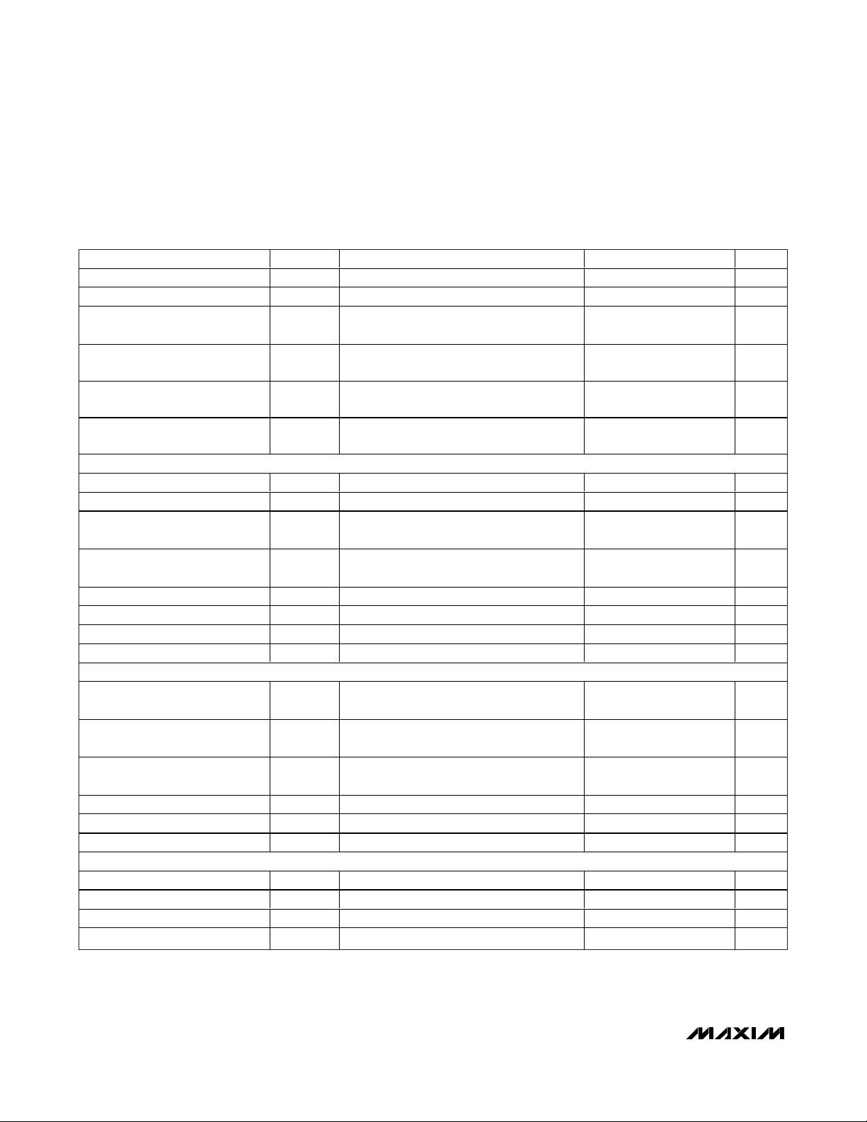
DC ELECTRICAL CHARACTERISTICS (continued)
(VCC= +3V to +4.5V, VL= +1.65V to +3.6V, C
FLYING
= 100nF, C
VBUS
= 1µF, ESR
CVBUS
= 0.1Ω (max), TA= T
MIN
to T
MAX
, unless
otherwise noted. Typical values are at V
CC
= +3.7V, VL= +2.5V, TA= +25°C.) (Note 2)
PARAMETER SYM B O L CONDITIONS MIN TYP MAX UNITS
Switching Frequency f
V
Leakage Voltage V
BUS
V
Rise Time
BUS
V
Pulldown Resistance
BUS
V
Pullup Resistance
BUS
V
Input Impedance Z
BUS
SW
INVBUS
COMPARATOR SPECIFICATIONS
V
V al i d C om p ar ator Thr eshol d V
B U S
V
V al i d C om p ar ator H yster esi sV
B U S
Session-Valid Comparator
Threshold
Session-End Comparator
Threshold
TH-VBUS
HYS-VBUS
V
TH-
SESS_VLD
V
TH-
SESS_END
dp_hi Comparator Threshold 0.8 1.3 2.0 V
dm_hi Comparator Threshold 0.8 1.3 2.0 V
cr_int Pulse Width 750 ns
cr_int Comparator Threshold 0.4 0.5 0.6 V
ID_IN SPECIFICATIONS
ID_IN Input Voltage for Car Kit
ID_IN Input Voltage for A Device
ID_IN Input Voltage for B Device
ID_IN Input Impedance Z
ID_IN
ID_IN Input Leakage Current ID_IN = V
ID_IN Pulldown Resistance id_pulldown = 1 150 300 Ω
TERMINATING RESISTOR SPECIFICATIONS (D+, D-)
D+ Pulldown Resistor dp_pulldown = 1 14.25 15 15.75 kΩ
D- Pulldown Resistor dm_pulldown = 1 14.25 15 15.75 kΩ
D+ Pullup Resistor dp_pullup = 1 1.425 1.5 1.575 kΩ
D- Pullup Resistor dm_pullup = 1 1.425 1.5 1.575 kΩ
VBUS_DRV
C
= 10µF, I
VBUS
from 0 to +4.4V
V
VBUS_DISCHRG
V
VBUS_CHRG
V
VBUS_CHRG
V
VBUS_DISCHRG
V
VBUS_DISCHRG
V
VBUS_CHRG
390 kHz
= 0 0.2 V
= 8mA, measured
VBUS
= 1, V
= 0
= 1, V
= 0
= 0, V
= 0
VBUS_DRV
VBUS_DRV
VBUS_DRV
= 0,
= 0,
= 0,
3.8 5 6.5 kΩ
650 930 1250 Ω
40 70 100 kΩ
100 ms
4.4 4.6 4.8 V
50 mV
0.8 1.4 2.0 V
0.2 0.5 0.8 V
0.2 x
V
CC
0.8 x
V
CC
0.1 x
V
CC
0.9 x
V
CC
70 100 130 kΩ
CC
-1 +1 µA
V
V
V
Page 5
MAX3301E/MAX3302E
USB On-the-Go Transceivers and Charge Pumps
_______________________________________________________________________________________ 5
TIMING CHARACTERISTICS
(VCC= +3V to +4.5V, VL= +1.65V to +3.6V, C
FLYING
= 100nF, C
VBUS
= 1µF, ESR
CVBUS
= 0.1Ω (max), TA= T
MIN
to T
MAX
, unless
otherwise noted. Typical values are at V
CC
= +3.7V, VL= +2.5V, TA= +25°C.) (Note 2)
PARAMETER SYM B O L CONDITIONS MIN TYP MAX UNITS
TRANSMITTER CHARACTERISTICS (FULL-SPEED MODE)
D+, D- Rise Time t
D+, D- Fall Time t
R
F
Rise-/Fall-Time Matching Figures 2 and 5 (Note 3) 90 110 %
Output-Signal Crossover Voltage V
CRS_F
TRANSMITTER CHARACTERISTICS (LOW-SPEED MODE)
D+, D- Rise Time t
D+, D- Fall Time t
R
F
Rise-/Fall-Time Matching Figures 2 and 5 80 125 %
Output-Signal Crossover Voltage V
CRS_L
TRANSMITTER TIMING (FULL-SPEED MODE)
t
Driver Propagation Delay
(DAT_VP, SE0_VM to D+, D-)
Driver Disable Delay t
Driver Enable Delay t
PLH
t
PHL
PDZ
PZD
TRANSMITTER TIMING (LOW-SPEED MODE) (Low-speed delay timing is dominated by the slow rise and fall times.)
SPEED-INDEPENDENT TIMING CHARACTERISTICS
Receiver Disable Delay t
Receiver Enable Delay t
PVZ
PZV
D+ Pullup Assertion Time During HNP 3 µs
RCV Rise Time t
RCV Fall Time t
Differential-Receiver Propagation
Delay
Single-Ended-Receiver
Propagation Delay
t
PHL
t
PHL
R
F
, t
PLH
, t
PLH
Interrupt Propagation Delay 100 µs
V
BUS_CHRG
Propagation Delay Dominated by the V
Time to Exit Shutdown 1µs
Shutdown Delay 10 µs
Figures 2 and 5 4 20 ns
Figures 2 and 5 4 20 ns
Figures 2, 6, and 7 (Note 3) 1.3 2.0 V
Figures 2 and 5 75 300 ns
Figures 2 and 5 75 300 ns
Figures 2, 6, and 7 1.3 2.0 V
Low-to-high, Figures 2 and 6 25
High-to-low, Figures 2 and 6 25
Figures 1 and 8 25 ns
Figures 2 and 8 25 ns
Figure 4 30 ns
Figure 4 30 ns
Figures 3 and 5, CL = 15pF 4 ns
Figures 3 and 5, CL = 15pF 4 ns
Figures 3 and 10, |D+ - D-| to DAT_VP 30
Figures 3 and 9, |D+ - D-| to RCV 30
Figures 3 and 9, D+, D- to DAT_VP,
SE0_VM
rise time 0.2 µs
BUS
30 ns
ns
ns
Page 6
MAX3301E/MAX3302E
USB On-the-Go Transceivers and Charge Pumps
6 _______________________________________________________________________________________
I2C-/SMBus™-COMPATIBLE TIMING SPECIFICATIONS
(VCC= +3V to +4.5V, VL= +1.65V to +3.6V, C
FLYING
= 100nF, C
VBUS
= 1µF, ESR
CVBUS
= 0.1Ω (max), TA= T
MIN
to T
MAX
, unless
otherwise noted. Typical values are at V
CC
= +3.7V, VL= +2.5V, TA= +25°C.) (Note 2)
Note 2: Parameters are 100% production tested at +25°C. Limits over temperature are guaranteed by design.
Note 3: Guaranteed by bench characterization. Limits are not production tested.
Note 4: A master device must provide a hold time of at least 300ns for the SDA signal to bridge the undefined region of SCL’s falling
edge.
Note 5: C
B
is the total capacitance of one bus line in pF, tested with CB= 400pF.
Note 6: Input filters on SDA, SCL, and ADD suppress noise spikes of less than 50ns.
SMBus is a trademark of Intel Corporation.
PARAMETER SYM B O L CONDITIONS MIN TYP MAX UNITS
Serial Clock Frequency f
Bus-Free Time Between Stop and
Start Conditions
Start-Condition Hold Time t
Stop-Condition Setup Time t
Clock Low Period t
Clock High Period t
Data Setup Time t
Data Hold Time t
Rise Time of SDA and SCL t
Fall Time of SDA and SCL t
Capacitive Load for each Bus
Line
SCL
t
BUF
HD_STA
SU_STO
LOW
HIGH
SU_DAT
HD_DAT
R
F
C
B
SDA AND SCL I/O STAGE CHARACTERISTICS
Input-Voltage Low V
Input-Voltage High V
SDA Output-Voltage Low V
Pulse Width of Suppressed Spike t
IL
IH
OL
SP
400 kHz
1.3 µs
0.6 µs
0.6 µs
1.3 µs
0.6 µs
100 ns
(Note 4) 0.9 µs
20 +
(Note 5)
0.1 x
C
B
300 ns
Measured from 0.3 x VL to 0.7 x VL (Note 5) 300 ns
400 pF
0.3 x
V
L
0.7 x
V
L
I
= 3mA 0.4 V
SINK
(Note 6) 50 ns
V
V
Page 7
DRIVER PROPAGATION DELAY HIGH-TO-LOW
(FULL-SPEED MODE)
MAX3301E toc09
4ns/div
D+
1V/div
D1V/div
DAT_VP
1V/div
DRIVER PROPAGATION DELAY LOW-TO-HIGH
(LOW-SPEED MODE)
MAX3301E toc08
100ns/div
D1V/div
D+
1V/div
DAT_VP
1V/div
DRIVER PROPAGATION DELAY HIGH-TO-LOW
(LOW-SPEED MODE)
MAX3301E toc07
100ns/div
D+
1V/div
D1V/div
DAT_VP
1V/div
TIME TO EXIT SHUTDOWN
MAX3301E toc05
4μs/div
D1V/div
D+
1V/div
SCL
1V/div
V
BUS
DURING SRP
MAX3301E toc06
20ns/div
V
BUS
1V/div
V
BUS
1V/div
C
VBUS
> 96μF
C
VBUS
> 13μF
TIME TO ENTER SHUTDOWN
MAX3301E toc04
100ns/div
D+
1V/div
D1V/div
SCL
2V/div
V
BUS
OUTPUT VOLTAGE
vs. INPUT VOLTAGE (V
CC
)
MAX3301E toc03
INPUT VOLTAGE (VCC) (V)
V
BUS
OUTPUT VOLTAGE (V)
5.55.04.54.03.53.0
4.75
5.00
5.25
5.50
5.75
4.50
2.5 6.0
LINEAR REGULATOR
POWERED BY V
CC
I
VBUS
= 8mA
I
VBUS
= 0
V
BUS
OUTPUT VOLTAGE
vs. V
BUS
OUTPUT CURRENT
MAX3301E toc02
V
BUS
OUTPUT CURRENT (mA)
V
BUS
OUTPUT VOLTAGE (V)
252015105
4.25
4.50
4.75
5.00
5.25
5.50
4.00
030
VCC = 3.0V
V
CC
= 4.2V
LINEAR REGULATOR
POWERED BY V
CC
INPUT CURRENT (ICC)
vs. V
BUS
OUTPUT CURRENT
MAX3301E toc01
V
BUS
OUTPUT CURRENT (mA)
INPUT CURRENT (I
CC
) (mA)
161284
10
20
30
40
50
0
020
VCC = 3.3V
V
CC
= 4.2V
LINEAR REGULATOR
POWERED BY V
CC
MAX3301E/MAX3302E
USB On-the-Go Transceivers and Charge Pumps
_______________________________________________________________________________________
7
Typical Operating Characteristics
(Typical operating circuit, VCC= +3.7V, VL= +2.5V, C
FLYING
= 100nF, TA= +25°C, unless otherwise noted.)
Page 8
SUPPLY CURRENT
vs. TEMPERATURE
MAX3301E toc15
TEMPERATURE (°C)
SUPPLY CURRENT (mA)
603510-15
0.2
0.4
0.6
0.8
1.0
0
-40 85
V
BUS
OFF
FULL-SPEED IDLE
VCC = 3.3V
VCC = 4.2V
DRIVER DISABLE DELAY
(LOW-SPEED MODE)
MAX3301E toc14
10ns/div
D+
1V/div
D1V/div
OE/INT
1V/div
DRIVER ENABLE DELAY
(LOW-SPEED MODE)
MAX3301E toc13
100ns/div
D1V/div
D+
1V/div
CD+ = CD- = 400pF
OE/INT
1V/div
DRIVER DISABLE DELAY
(FULL-SPEED MODE)
MAX3301E toc12
10ns/div
D+
1V/div
D1V/div
OE/INT
1V/div
DRIVER ENABLE DELAY
(FULL-SPEED MODE)
MAX3301E toc11
10ns/div
D1V/div
D+
1V/div
OE/INT
1V/div
DRIVER PROPAGATION DELAY LOW-TO-HIGH
(FULL-SPEED MODE)
MAX3301E toc10
4ns/div
D1V/div
D+
1V/div
DAT_VP
1V/div
MAX3301E/MAX3302E
USB On-the-Go Transceivers and Charge Pumps
8 _______________________________________________________________________________________
Typical Operating Characteristics (continued)
(Typical operating circuit, VCC= +3.7V, VL= +2.5V, C
FLYING
= 100nF, TA= +25°C, unless otherwise noted.)
Page 9
MAX3301E/MAX3302E
USB On-the-Go Transceivers and Charge Pumps
_______________________________________________________________________________________ 9
Pin Description
PIN
MAX3302E
28-PIN TQFN
1 2 D2 DAT_VP
2, 25 3, 29 D1, E3 V
3, 9, 23
4 5 C1 C- Charge-Pump Flying-Capacitor Negative Terminal
5 6 C2 SE0_VM
6, 18 7, 21 B1, C5 GND Ground
7 8 A1 SDA I2C-Compatible Serial Data Interface. Open-drain data input/output.
8 10 B2 SCL I2C-Compatible Serial Clock Input
10 11 A2 OE/INT
11 13 A3 RCV
12 14 B3 SPD
13 15 A4 V
14 16 A5 SUS
MAX3301E
32-PIN TQFN
1, 4, 9, 12, 17,
25, 28
UCSP/
WLP
NAME FUNCTION
System-Side Data Input/Output. DAT_VP is an input if OE/INT is logic 0.
DAT_VP is an output if OE/INT is logic 1. Program the function of DAT_VP
with the dat_se0 bit (bit 2 of control register 1, see Table 7).
Input Power Supply. Connect a +3V to +4.5V supply to VCC and bypass to
GND with a 1µF capacitor. The supply range enables direct powering from
CC
one Li+ battery.
— N.C. No Connection. Not internally connected.
System-Side Data Input/Output. SE0_VM is an input if OE/INT is logic 0.
SE0_VM is an output if OE/INT is logic 1. Program the function of SE0_VM
with the dat_se0 bit (bit 2 of control register 1, see Table 7).
O utp ut E nab l e. O E/INT contr ol s the i np ut or outp ut status of D AT_V P /S E 0_V M
and D + /D - . W hen O E/INT i s l og i c 0, the d evi ce i s i n tr ansm i t m od e. W hen
O E/INT i s l og i c 1, the d evi ce i s i n r ecei ve m od e. When i n susp end m od e,
O E/INT can b e p r og r am m ed to functi on as an i nter r up t outp ut that d etects the
sam e i nter r up ts as
7) enab l es and d i sab l es the i nter r up t ci r cui tr y of O E/INT. The i r q _m od e b i t ( b i t 1
of sp eci al - functi on r eg i ster 2, see Tab l e 15) p r og r am s the outp ut confi g ur ati on
of INT and O E/INT as op en- d r ai n or p ush- p ul l .
D+ and D- Differential Receiver Output. In receive mode (see Table 4), when
D+ is high and D- is low, RCV is high. In receive mode, when D+ is low and
D- is high, RCV is low. RCV is low in suspend mode.
Speed-Selector Input. Connect SPD to GND to select the low-speed data rate
(1.5Mbps). Connect SPD to V
Disable the SPD input by writing a 1 to spd_susp_ctl (bit 1 in special-function
register 1, see Table 14). The speed bit (bit 0 of control register 1, see Table
7) determines the maximum data rate of the MAX3301E/MAX3302E when the
SPD input is disabled.
System-Side Logic-Supply Input. Connect to the system’s logic-level power
supply, +1.65V to +3.6V. This sets the maximum output levels of the logic
L
outputs and the input thresholds of the logic inputs. Bypass to GND with a
0.1µF capacitor.
Active-High Suspend Input. Drive SUS low for normal USB operation. Drive
SUS high to enable suspend mode. RCV asserts low in suspend mode.
Disable the SUS input by writing a 1 to spd_susp_ctl (bit 1 in special-function
register 1, see Table 14). The suspend bit (bit 1 of control register 1, see
Table 7) determines the operating mode of the MAX3301E/MAX3302E when
the SUS input is disabled.
INT. The oe_i nt_en b i t ( b i t 5 of contr ol r eg i ster 1, see Tab l e
to select the full-speed data rate (12Mbps).
L
Page 10
MAX3301E/MAX3302E
USB On-the-Go Transceivers and Charge Pumps
10 ______________________________________________________________________________________
Pin Description (continued)
Test Circuits and Timing Diagrams
Figure 1. Load for Disable Time Measurement
Figure 2. Load for Enable Time, Transmitter Propagation Delay,
and Transmitter Rise/Fall Times
PIN
MAX3302E
28-PIN TQFN
MAX3301E
32-PIN TQFN
UCSP/
WLP
15 18 B4 INT
NAME FUNCTION
Active-Low Interrupt Source. Program the INT output as push-pull or open-
drain with the irq_mode bit (bit 1 of special-function register 2, see Tables 15
and 16).
16 19 B5 RESET
Active-Low Reset Input. Drive RESET low to asynchronously reset the
MAX3301E/MAX3302E.
17 20 C3 ADD I2C-Interface Address Selection Input. (See Table 5.)
19 22 C4 ID_IN
20 23 D5 D-
21 24 E5 D+
22 26 D4 VM
ID Input. ID_IN is internally pulled up to V
ID bits 3 and 5 of the interrupt source register (see Table 10).
USB Differential Data Input/Output. Connect D- to the D- terminal of the USB
connector through a 27.4Ω ±1% series resistor.
USB Differential Data Input/Output. Connect D+ to the D+ terminal of the USB
connector through a 27.4Ω ±1% series resistor.
Single-Ended Receiver Output. VM functions as a receiver output in all
operating modes. VM duplicates D-.
USB Transceiver Regulated Output Voltage. TRM provides a regulated 3.3V
output. Bypass TRM to GND with a 1µF ceramic capacitor installed as close
to the device as possible. TRM normally derives power from V
24 27 E4 TRM
provides power to internal circuitry and provides the pullup voltage for the
internal USB pullup resistor. Do not use TRM to power external circuitry. The
reg_sel bit (bit 3 of special-function register 2, see Table 15 and Table 16)
controls the TRM power source with software.
26 30 D3 VP
Single-Ended Receiver Output. VP functions as a receiver output in all
operating modes. VP duplicates D+.
USB Bus Power. Use V
27 31 E2 V
to power the internal linear regulator. Bits 5 to 7 of control register 2 (see
BUS
Table 8) control the charging and discharging functions of V
28 32 E1 C+ Charge-Pump Flying-Capacitor Positive Terminal
EP EP — EP Exposed Paddle. Connect EP to GND or leave unconnected.
. The state of ID_IN determines
CC
. TRM
CC
as an output to power the USB bus, or as an input
BUS
.
BUS
TEST POINT
27.4Ω 220Ω
DUT
D+/D-
C
LOAD FOR DISABLE TIME (D+/D-) MEASUREMENT
V = 0 FOR t
V = V
C
C
L
.
PHZ
FOR t
TRM
= 50pF FOR FULL SPEED.
L
= 200pF TO 600pF FOR LOW SPEED.
L
V
.
PLZ
27.4Ω
DUT
D+/D-
15kΩ
TEST POINT
LOAD FOR
1) ENABLE TIME (D+/D-) MEASUREMENT
2) DAT_VP/SEO_VM TO D+/D- PROPAGATION DELAY
3) D+/D- RISE/FALL TIMES
= 50pF FOR FULL SPEED.
C
C
L
L
= 200pF TO 600pF FOR LOW SPEED.
C
L
Page 11
MAX3301E/MAX3302E
USB On-the-Go Transceivers and Charge Pumps
______________________________________________________________________________________ 11
Test Circuits and Timing Diagrams (continued)
Figure 5. Rise and Fall Times
Figure 6. Timing of DAT_VP, SE0_VM to D+, D- in VP_VM
Mode (dat_se0 = 0)
Figure 7. Timing of DAT_VP, SE0_VM to D+/D- in DAT_SE0
Mode (dat_se0 = 1)
Figure 8. Enable and Disable Timing
Figure 9. D+/D- to RCV, DAT_VP, SE0_VM Propagation Delays
(VP_VM Mode)
Figure 10. D+/D- to DAT_VP, SE0_VM Propagation Delays
(DAT_SE0 Mode)
Figure 3. Load for Receiver Propagation Delay and Receiver
Rise/Fall Times
Figure 4. Load for DAT_VP, SE0_VM Enable/Disable Time
Measurements
TEST POINT
LOAD FOR
DUT
RCV, VP, VM,
DAT_VP,
SEO_VM
V
V
DAT_VP
SE0_VM
1) D+/D- TO RCV/VP/VM/DAT_VP/SEO_VM PROPAGATION DELAYS
2) RCV/VP/VM/DAT_VP/SEO_VM RISE/FALL TIMES (C
C
L
TEST POINT
DUT
DAT_VP
SEO_VM
OH
OL
270Ω
V = 2/3 x V
t
R
t
PHL
t
F
t
PLH
90%
10%
= 15pF)
L
L
V
L
VL
OE/INT
0V
V
OH
/ 2 VL
t
PZD
/ 2
t
PDZ
- 0.3V
V
OHD
D+ OR D-
V
+ 0.3V
V
OL
OLD
D+
D-
RCV
DAT_VP
SE0_VM
D+/D- RISE/FALL TIMES ≤ 8ns, VL = 1.8V, 2.5V, OR 3.3V
t
PHL
t
PHL
t
PLH
3V
0V
t
PLH
V
L
VL / 2
0V
t
PLH
V
L
V
/ 2
L
0V
t
PHL
V
L
/ 2
V
L
0V
D+
V
OHD
V
, V
CRS_F
D-
V
OLD
CRS_L
V
CRS_F
, V
CRS_L
DAT_VP
SE0_VM
D+
V
D-
V
OHD
OLD
t
PHL
V
CRS_F
, V
t
CRS_L
PLH
V
CRS_F
, V
CRS_L
D+
D-
t
DAT_VP
SE0_VM
D+/D- RISE/FALL TIMES ≤ 8ns, VL = 1.8V, 2.5V, OR 3.3V
PHL
t
PLH
3V
0V
V
L
VL / 2
0V
Page 12
MAX3301E/MAX3302E
USB On-the-Go Transceivers and Charge Pumps
12 ______________________________________________________________________________________
Block Diagram
Figure 11. Block Diagram
ADD
INT
RESET
SCL
SDA
SERIAL
CONTROLLER
DAT_VP
SE0_VM
OE/INT
VP
VM
RCV
V
GND
SPD
CC
V
L
POWER
BLOCK
LEVEL
TRANSLATOR
ID
DETECTOR
V
BUS
CHARGE PUMP
V
BUS
COMPARATORS
LINEAR
REGULATOR
PULLUP/PULLDOWN
RESISTORS
CAR KIT INTERRUPT
DETECTOR
SE
D+
SE
D-
DIFF
TX
DIFF
RX
ID_IN
C+
C-
V
BUS
TRM
D+
D-
SUS
MAX3301E
MAX3302E
Page 13

MAX3301E/MAX3302E
USB On-the-Go Transceivers and Charge Pumps
______________________________________________________________________________________ 13
Detailed Description
The USB OTG specification defines a dual-role USB
device that acts either as an A device or as a B device.
The A device supplies power on V
BUS
and initially
serves as the USB host. The B device serves as the initial peripheral and requires circuitry to monitor and pulse
V
BUS
. These initial roles can be reversed using HNP.
The MAX3301E/MAX3302E combine a low- and fullspeed USB transceiver with additional circuitry required
by a dual-role device. The MAX3301E/MAX3302E
employ flexible switching circuitry to enable the device
to act as a dedicated host or peripheral USB transceiver. For example, the charge pump can be turned off and
the internal regulator can be powered from V
BUS
for
bus-powered peripheral applications.
The
Selector Guide
shows the differences between the
MAX3301E and MAX3302E. The MAX3301E powers up
in its lowest power state and must be turned on by setting the sdwn bit to 0. The MAX3302E powers up in the
operational, VP/VM USB mode. This allows a microprocessor (µP) to use the USB port for power-on bootup, without having to access I
2
C. To put the MAX3302E
into low-power shutdown, set the sdwn bit to 0. In the
MAX3302E, special-function register 2 can be
addressed at I2C register location 10h, 11h (as well as
locations 16h, 17h) to support USB OTG serial-interface
engine (SIE) implementations that are limited to I2C
register addresses between 0h and 15h.
Transceiver
The MAX3301E/MAX3302E transceiver complies with
the USB version 2.0 specification, and operates at fullspeed (12Mbps) and low-speed (1.5Mbps) data rates.
Set the data rate with the SPD input. Set the direction of
data transfer with the OE/INT input. Alternatively, control
transceiver operation with control register 1 (Table 7)
and special-function registers 1 and 2 (see Tables 14,
15, and 16).
Level Shifters
Internal level shifters allow the system-side interface to
run at logic-supply voltages as low as +1.65V. Interface
logic signals are referenced to the voltage applied to
the logic-supply voltage, VL.
Charge Pump
The MAX3301E/MAX3302E’s OTG-compliant charge
pump operates with +3V to +4.5V input supply voltages
(VCC) and supplies a +4.8V to +5.25V OTG-compatible
output on V
BUS
while sourcing the 8mA or greater output current that an A device is required to supply.
Connect a 0.1µF flying capacitor between C+ and C-.
Bypass V
BUS
to GND with a 1µF to 6.5µF capacitor, in
accordance with USB OTG specifications. The charge
pump can be turned off to conserve power when not
used. Control of the charge pump is set through the
vbus_drv bit (bit 5) of control register 2 (see Table 8).
Linear Regulator (TRM)
An internal 3.3V linear regulator powers the transceiver
and the internal 1.5kΩ D+/D- pullup resistor. Under the
control of internal register bits, the linear regulator can be
powered from VCCor V
BUS
. The regulator power-supply
settings are controlled by the reg_sel bit (bit 3) in specialfunction register 2 (Tables 15 and 16). This flexibility
allows the system designer to configure the MAX3301E/
MAX3302E for virtually any USB power situation.
The output of the TRM is not a power supply. Do not use
as a power source for any external circuitry. Connect a
1.0µF (or greater) ceramic or plastic capacitor from TRM
to GND, as close to the device as possible.
V
BUS
Level-Detection Comparators
Comparators drive interrupt source register bits 0, 1,
and 7 (Table 10) to indicate important USB OTG V
BUS
voltage levels:
•V
BUS
is valid (vbus_vld)
• USB session is valid (sess_vld)
• USB session has ended (sess_end)
The vbus_valid comparator sets vbus_vld to 1 if V
BUS
is
higher than the V
BUS
valid comparator threshold. The
V
BUS
valid status bit (vbus_vld) is used by the A device
to determine if the B device is sinking too much current
(i.e., is not supported). The session_valid comparator
sets sess_vld to 1 if V
BUS
is higher than the session
valid comparator threshold. This status bit indicates that
a data transfer session is valid. The session_end comparator sets sess_end to 1 if V
BUS
is higher than the
Figure 12. Comparator Network Diagram
V
BUS
V
TH-VBUS
V
TH-SESS_VLD
V
TH-SESS_END
VBUS_VLD
SESS_VLD
SESS_END
Page 14

MAX3301E/MAX3302E
USB On-the-Go Transceivers and Charge Pumps
14 ______________________________________________________________________________________
Table 1. Functional Blocks Enabled During Specific Operating Modes
= Enabled.
X
= Disabled.
1. For the MAX3301E, enter shutdown mode by writing a 1 to sdwn (bit 0 of special-function register 2). For the MAX3302E, enter
shutdown mode by writing a 0 to sdwn (bit 0 of special-function register 2).
2. Enter interrupt shutdown mode by writing a 1 to int_sdwn (bit 0 of special-function register 1).
3. Enter suspend mode by writing a 1 to spd_susp_ctl (bit 1 of special-function register 1) and suspend (bit 1 of control register 1), or
by writing a 0 to spd_susp_ctl (bit 1 of special-function register 1) and driving SUS high.
session end comparator threshold. Figure 12 shows the
level-detector comparators. The interrupt-enable registers (Tables 12 and 13) determine whether a falling or
rising edge of V
BUS
asserts these status bits.
ID_IN
The USB OTG specification defines an ID input that
determines which dual-role device is the default host.
An OTG cable connects ID to ground in the connector
of one end and is left unconnected in the other end.
Whichever dual-role device receives the grounded end
becomes the A device. The MAX3301E/MAX3302E provide an internal pullup resistor on ID_IN. Internal comparators detect if ID_IN is grounded or left floating.
Interrupt Logic
When OTG events require action, the MAX3301E/
MAX3302E provide an interrupt output signal on INT.
Alternatively, OE/INT can be configured to act as an
interrupt output while the device operates in USB suspend mode. Program INT and OE/INT as open-drain or
push-pull interrupts with irq_mode (bit 1 of special-function register 2, see Tables 15 and 16).
V
BUS
Power Control
V
BUS
is a dual-function port that powers the USB bus
and/or provides a power source for the internal linear regulator. The V
BUS
power-control block performs the various
switching functions required by an OTG dual-role device.
These actions are programmed by the system logic using
bits 5 to 7 of control register 2 (see Table 8) to:
• Discharge V
BUS
through a resistor
• Provide power-on or receive power from V
BUS
• Charge V
BUS
through a resistor
The OTG supplement allows an A device to turn V
BUS
off when the bus is not being used to conserve power.
The B device can issue a request that a new session be
started using SRP. The B device must discharge V
BUS
to a level below the session-end threshold (0.8V) to
ensure that no session is in progress before initiating
SRP. Setting bit 6 of control register 2 to 1, discharges
V
BUS
to GND through a 5kΩ current-limiting resistor.
When V
BUS
has discharged, the resistor is removed
from the circuit by resetting bit 6 of control register 2.
An OTG A device is required to supply power on V
BUS
.
The MAX3301E/MAX3302E provide power to V
BUS
from
VCCor from the internal charge pump. Set bit 5 in control
register 2 to 1 in both cases. Bit 5 in control register 2
controls a current-limited switch, preventing damage to
the device in the event of a V
BUS
short circuit.
An OTG B device (peripheral mode) can request a session using SRP. One of the steps in implementing SRP
requires pulsing V
BUS
high for a controlled time. A 930Ω
resistor limits the current according to the OTG specification. Pulse V
BUS
through the pullup resistor by assert-
ing bit 7 of control register 2. Prior to pulsing V
BUS
(bit
7), a B device first connects an internal pulldown resistor to discharge V
BUS
below the session-end threshold.
The discharge current is limited by the 5kΩ resistor and
set by bit 6 of control register 2. An OTG A device must
MODE I2C ID_IN
Shutdown1✓ X X X X X X X XXXX
Interrupt
Shutdown
Suspend
Normal
Operating
✓✓ X ✓ XX✓✓XXXX
2
3
✓✓✓✓✓✓✓✓✓✓X ✓
✓✓✓✓✓✓✓✓✓✓✓✓
sess_end
COMP
sess _vld
COMP
vbus_ vld
COMP
cr_int
COMP
dp_hi
COMP
dm_hi
COMP
TRM TX
DIFFRXSE
RX
Page 15

MAX3301E/MAX3302E
USB On-the-Go Transceivers and Charge Pumps
______________________________________________________________________________________ 15
supply 5V power and at least 8mA on V
BUS
. Setting bit
5 of control register 2 turns on the V
BUS
charge pump.
Operating Modes
The MAX3301E/MAX3302E have four operating modes to
optimize power consumption. Only the I
2
C interface
remains active in shutdown mode, reducing supply current to 1µA. The I2C interface, the ID_IN port, and the
session-valid comparator all remain active in interrupt
shutdown mode. RCV asserts low in suspend mode; however, all other circuitry remains active. Table 1 lists the
active blocks’ power in each of the operating modes.
Applications Information
Data Transfer
Transmitting Data to the USB
The MAX3301E/MAX3302E transceiver features two
modes of transmission: DAT_SE0 or VP_VM (see Table 3).
Set the transmitting mode with dat_se0 (bit 2 in control
register 1, see Table 7). In DAT_SE0 mode with OE/INT
low, DAT_VP specifies data for the differential transceiver, and SE0_VM forces D+/D- to the single-ended zero
(SE0) state. In VP_VM mode with OE/INT low, DAT_VP
drives D+, and SE0_VM drives D-. The differential
receiver determines the state of RCV.
Receiving Data from the USB
The MAX3301E/MAX3302E transceiver features two
modes of receiving data: DAT_SE0 or VP_VM (see
Table 4). Set the receiving mode with dat_se0 (bit 2 in
control register 1, see Table 7). In DAT_SE0 mode with
OE/INT high, DAT_VP is the output of the differential
receiver and SE0_VM indicates that D+ and D- are both
logic-low. In VP_VM mode with OE/INT high, DAT_VP
provides the input logic level of D+ and SE0_VM provides the input logic level of D-. The differential receiver
determines the state of RCV. VP and VM echo D+ and
D-, respectively.
OE/INT
OE/INT controls the direction of communication. OE/INT
can also be programmed to act as an interrupt output
when in suspend mode. The output-enable portion controls the input or output status of DAT_VP/SE0_VM and
D+/D-. When OE/INT is a logic 0, DAT_VP and SE0_VM
function as inputs to the D+ and D- outputs in a method
depending on the status of dat_se0 (bit 2 in control register 1). When OE/INT is a logic 1, DAT_VP and SE0_VM
indicate the activity of D+ and D-.
OE/INT functions as an interrupt output when the
MAX3301E/MAX3302E is in suspend mode and
oe_int_en = 1 (bit 5 in control register 1, see Table 7). In
this mode, OE/INT detects the same interrupts as INT.
Set irq_mode (bit 1 in special-function register 2, see
Tables 15 and 16) to 0 to program OE/INT as an opendrain interrupt output. Set irq_mode to 1 to configure
OE/INT as a push-pull interrupt output.
RCV
RCV monitors D+ and D- when receiving data. RCV is a
logic 1 for D+ high and D- low. RCV is a logic 0 for D+
low and D- high. RCV retains its last valid state when D+
and D- are both low (single-ended zero, or SE0). RCV
asserts low in suspend mode. Table 4 shows the state
of RCV.
SPD
Use hardware or software to control the slew rate of the
D+ and D- terminals. The SPD input sets the slew rate of
the MAX3301E/MAX3302E when spd_susp_ctl (bit 1 in
special-function register 1, see Table 14) is 0. Drive SPD
low to select low-speed mode (1.5Mbps). Drive SPD
high to select full-speed mode (12Mbps). Alternatively,
when spd_susp_ctl (bit 1 of special-function register 1)
is 1, software controls the slew rate. The SPD input is
ignored when using software to control the data rate.
The speed bit (bit 0 of control register 1, see Table 7)
sets the slew rate when spd_susp_ctl = 1.
SUS
Use hardware or software to control the suspend mode
of the MAX3301E/MAX3302E. Set spd_susp_ctl (bit 1 of
special-function register 1, see Table 14) to 0 to allow
the SUS input to enable and disable the suspend mode
of the MAX3301E/MAX3302E. Drive SUS low for normal
operation. Drive SUS high to enable suspend mode.
RCV asserts low in suspend mode while all other circuitry remains active.
Alternatively, when the spd_susp_ctl bit (bit 1 of specialfunction register 1) is set to 1, software controls the suspend mode. Set the suspend bit (bit 1 of control register
1, see Table 7) to 1 to enable suspend mode. Set the
suspend bit to 0 to resume normal operation. The SUS
input is ignored when using software to control suspend
mode. The MAX3301E/MAX3302E must be in full-speed
mode (SPD = high or speed = 1) to issue a remote
wake-up from the device when in suspend mode.
RESET
The active-low RESET input allows the MAX3301E/
MAX3302E to be asynchronously reset without cycling
the power supply. Drive RESET low to reset the internal
registers (see Tables 7–16 for the default power-up
states). Drive RESET high for normal operation.
Page 16

MAX3301E/MAX3302E
USB On-the-Go Transceivers and Charge Pumps
16 ______________________________________________________________________________________
2-Wire I2C-Compatible Serial Interface
A register file controls the various internal switches and
operating modes of the MAX3301E/MAX3302E through
a simple 2-wire interface operating at clock rates up to
400kHz. This interface supports data bursting, where
multiple data phases can follow a single address phase.
UART Mode
Set uart_en (bit 6 in control register 1) to 1 to place the
MAX3301E/MAX3302E in UART mode. D+ transfers
data to DAT_VP and SE0_VM transfers data to D- in
UART mode.
General-Purpose Buffer Mode
Set gp_en (bit 7 in special-function register 1) and
dat_se0 (bit 2 in control register 1) to 1, set uart_en (bit 6
in control register 1) to 0, and drive OE/INT low to place
the MAX3301E/MAX3302E in general-purpose buffer
mode. Control the direction of data transfer with dminus_dir and dplus_dir (bits 3 and 4 of special-function
register 1, see Tables 2 and 14).
Serial Addressing
The MAX3301E/MAX3302E operate as a slave device
that sends and receives control and status signals
through an I2C-compatible 2-wire interface. The interface uses a serial data line (SDA) and a serial clock line
(SCL) to achieve bidirectional communication between
master(s) and slave(s). A master (typically a microcontroller) initiates all data transfers to and from the
MAX3301E/MAX3302E and generates the SCL clock
that synchronizes the data transfer (Figure 13).
The MAX3301E/MAX3302E SDA line operates as both an
input and as an open-drain output. SDA requires a
pullup resistor, typically 4.7kΩ. The MAX3301E/
MAX3302E SCL line only operates as an input. SCL
requires a pullup resistor if there are multiple masters on
the 2-wire interface, or if the master in a single-master
system has an open-drain SCL output.
Each transmission consists of a start condition (see
Figure 14) sent by a master device, the MAX3301E/
MAX3302E 7-bit slave address (determined by the state
of ADD), plus an R/W bit (see Figure 15), a register
address byte, one or more data bytes, and a stop condition (see Figure 14).
Table 2. Setting the Direction of Data
Transfer in General-Purpose Buffer Mode
Figure 13. 2-Wire Serial-Interface Timing Details
dplus_dir dminus_ dir
00
01
10
11
DIRECTION OF DATA
TRANSFER
DAT_VP → D+
SE0_VM → D-
DAT_VP → D+
SE0_VM ← D-
DAT_VP ← D+
SE0_VM → D-
DAT_VP ← D+
SE0_VM ← D-
SDA
t
t
t
LOW
SCL
t
HD: STA
START
CONDITION
SU: DAT
t
HIGH
t
R
t
HD: DAT
t
F
SU: STA
REPEATED START
CONDITION
t
HD: STA
t
SU: STO
STOP
CONDITION
t
BUF
CONDITION
START
Page 17

MAX3301E/MAX3302E
USB On-the-Go Transceivers and Charge Pumps
______________________________________________________________________________________ 17
Table 3. Transmit Mode
Figure 14. Start and Stop Conditions
Figure 15. Slave Address
MODE
Functional
DAT_SE0
Functional
VP_VM
Suspend
SUS GP_EN
CONTROL PIN/BIT INPUT OUTPUT
OE/INT
DAT_SE0 DAT_VP SE0_VM D+ D-
000 1 0 0 0 1
000 1 1 0 1 0
000 1 0 1 0 0
000 1 1 1 0 0
000 0 0 0 0 0
U S B functi onal m od e
tr anscei ver and I
ar e ful l y functi onal
000 0 1 0 1 0
000 0 0 1 0 1
000 0 1 1 1 1
100 1 0 0 0 1
100 1 1 0 1 0
100 1 0 1 0 0
100 1 1 1 0 0
100 0 0 0 0 0
100 0 1 0 1 0
USB suspend mode
100 0 0 1 0 1
100 0 1 1 1 1
101 X X X
Driver is
Hi-Z
Driver is
Hi-Z
DESCRIPTION
2
C i nter face
Receiving 0 0 1 X X X
General-
purpose
X 1 0 1 See Table 2
buffer
SDA
SCL
CONDITION
S
START
P
STOP
CONDITION
SDA
SCL
START
1
MSB
0
0
1
Driver is
Hi-Z
Driver is
Hi-Z
See Table 4
General-purpose buffer
mode
0
0A0
LSB
R/W
ACK
Page 18

MAX3301E/MAX3302E
USB On-the-Go Transceivers and Charge Pumps
18 ______________________________________________________________________________________
Table 4. Receive Mode
Note 7: Enter suspend mode by driving SUS high or by writing a 1 to suspend (bit 1 in control register 1), depending on the status of
spd_susp_ctl in special-function register 1.
X = Don’t care.
CONTROL PIN/BIT INPUTS OUTPUTS
MODE
SUS
(NOTE 7)
GP_EN OE/INT DAT_SE0 BI_DI D+ D- DAT_VP SE0 _ VM RCV VP VM
001 1100
001 11101 0 1
Functional
DAT_SE0
Functional
VP_VM
General-
purpose buffer
Transmitting
(see Table 3)
001 11010 0 0
0 0 1 1 1 1 1 Undefined 0 Undefined
101 11000 1 0
101 11101 0 0
101 11010 0 0
101 11111 0 0
001 01000 0
001 01101 0 1
001 01010 1 0
0 0 1 0 1 1 1 1 1 Undefined
101 01000 0 0
101 01101 0 0
101 01010 1 0
101 01111 1 0
X 1 X X X See Table 2 0
XX0 XX — 0
Last value
of DAT_VP
1
Last value
of RCV
Last value
of RCV
EchoD+Echo
D-
Unidirectional
(transmitter
only)
XXX X0 — 0
Page 19

MAX3301E/MAX3302E
USB On-the-Go Transceivers and Charge Pumps
______________________________________________________________________________________ 19
Start and Stop Conditions
Both SCL and SDA assert high when the interface is not
busy. A master device signals the beginning of a transmission with a start (S) condition by transitioning SDA
from high to low while SCL is high. The master issues a
stop (P) condition by transitioning SDA from low to high
while SCL is high. The bus is then free for another transmission (see Figure 14).
Bit Transfer
One data bit is transferred during each clock pulse. The
data on SDA must remain stable while SCL is high (see
Figure 16).
Acknowledge
The acknowledge bit (ACK) is the 9th bit attached to
any 8-bit data word. ACK is always generated by the
receiving device. The MAX3301E/MAX3302E generate
an ACK when receiving an address or data by pulling
SDA low during the ninth clock period. When transmitting data, the MAX3301E/MAX3302E wait for the receiving device to generate an ACK. Monitoring ACK allows
for detection of unsuccessful data transfers. An unsuccessful data transfer occurs if a receiving device is busy
or if a system fault has occurred. In the event of an
unsuccessful data transfer, the bus master should reattempt communication at a later time.
Slave Address
A bus master initiates communication with a slave
device by issuing a START condition followed by the 7bit slave address (see Figure 15). When idle, the
MAX3301E/MAX3302E wait for a START condition followed by its slave address. The LSB of the address
word is the read/write (R/W) bit. R/W indicates whether
the master is writing to or reading from the
MAX3301E/MAX3302E (R/W = 0 selects the write condition, R/W = 1 selects the read condition). After
receiving the proper address, the MAX3301E/
MAX3302E issue an ACK.
The MAX3301E/MAX3302E have two possible addresses
(see Table 5). Address bits A6 through A1 are preset,
while a reset condition or an I2C general call address
loads the value of A0 from ADD. Connect ADD to GND to
set A0 to 0. Connect ADD to VLto set A0 to 1. This allows
up to two MAX3301E’s or two MAX3302E’s to share the
same bus.
Write Byte Format
Writing data to the MAX3301E/MAX3302E requires the
transmission of at least 3 bytes. The first byte consists of
the MAX3301E/MAX3302E’s 7-bit slave address, followed by a 0 (R/W bit). The second byte determines
which register is to be written to. The third byte is the
new data for the selected register. Subsequent bytes
are data for sequential registers. Figure 18 shows the
typical write byte format.
Read Byte Format
Reading data from the MAX3301E/MAX3302E requires
the transmission of at least 3 bytes. The first byte consists of the MAX3301E/MAX3302E’s slave address, followed by a 0 (R/W bit). The second byte selects the
register from which data is read. The third byte consists
Figure 16. Bit Transfer
Figure 17. Acknowledge
Figure 18. Write Byte Format
SDA
SCL
DATA LINE STABLE,
DATA VALID
CHANGE OF DATA
ALLOWED
START
CONDITION
SCL
SDA BY
TRANSMITTER
S
SDA BY
RECEIVER
S
A6 A5 A4 A3 A2 A1 A0 0
CLOCK PULSE FOR ACKNOWLEDGEMENT
12 8 9
SLAVE ADDRESS
(7 BITS)
R/W
A
MSB LSB
REGISTER ADDRESS
(8 BITS)
AAP
MSB LSB
DATA
(8 BITS)
Page 20

MAX3301E/MAX3302E
USB On-the-Go Transceivers and Charge Pumps
20 ______________________________________________________________________________________
of the MAX3301E/MAX3302E’s slave address, followed
by a 1 (R/W bit). The master then reads one or more
bytes of data. Figure 19 shows the typical read byte
format.
Burst-Mode Write Byte Format
The MAX3301E/MAX3302E allow a master device to
write to sequential registers without repeatedly sending
the slave address and register address each time. The
master first sends the slave address, followed by a 0 to
write data to the MAX3301E/MAX3302E. The
MAX3301E/MAX3302E send an acknowledge bit back
to the master. The master sends the 8-bit register
address and the MAX3301E/MAX3302E return an
acknowledge bit. The master writes a data byte to the
selected register and receives an acknowledge bit if a
supported register address has been chosen. The register address increments and is ready for the master to
send the next data byte. The MAX3301E/MAX3302E
send an acknowledge bit after each data byte. If an
unsupported register is selected, the MAX3301E/
MAX3302E send a NACK to the master and the register
index does not increment (see Figure 20).
Figure 20. Burst-Mode Write Byte Format
Figure 19. Read Byte Format
R/W: Read/write (R/W = 1: read; R/W = 0: write)
S: Start condition
RS: Repeated start condition
P: Stop condition
A: Acknowledge bit from the slave
NA: Not-acknowledged bit from the master
Blank: Master transmission
S
A6 A5 A4 A3 A2 A1 A0 0 0 0
RS
A6 A5 A4 A3 A2 A1 A0 1 1 00
SLAVE ADDRESS
(7 BITS)
SLAVE ADDRESS
(7 BITS)
S
A6 A5 A4 A3 A2 A1 A0 0
MSB LSB
SLAVE ADDRESS
(7 BITS)
DATA (K+1)
(8 BITS)
A
R/W
MSB LSB
A
MSB LSB
MAX3301E/MAX3302E RECOGNIZES
ITS ADDRESS
A
R/W
MSB LSB
R/W
A
MSB LSB
REGISTER ADDRESS (K)
(8 BITS)
DATA (K+2)
(8 BITS)
REGISTER ADDRESS
(8 BITS)
DATA
(8 BITS)
AA
MSB LSB
AA
MSB LSB
MAX3301E/MAX3302E SENDS
AN ACK
A
NA P
DATA (K)
(8 BITS)
DATA (K+N)
(8 BITS)
P
S
A6 A5 A4 A3 A2 A1 A0 0
SLAVE ADDRESS
(7 BITS)
R/W
UNSUPPORTED REGISTER ADDRESS (K)
A
MSB LSB
(8 BITS)
ANA
MSB LSB
MAX3301E/MAX3302E RECOGNIZES A WRITE TO AN
UNSUPPORTED LOCATION, THEN SENDS A NACK
DATA (K)
(8 BITS)
Page 21

MAX3301E/MAX3302E
USB On-the-Go Transceivers and Charge Pumps
______________________________________________________________________________________ 21
Figure 21. Burst-Mode Read Byte Format
Table 5. I2C Slave Address Map
S
A6 A5 A4 A3 A2 A1 A0 0
S
A6 A5 A4 A3 A2 A1 A0 1
MSB LSB
S
A6 A5 A4 A3 A2 A1 A0 0
S
A6 A5 A4 A3 A2 A1 A0 1
SLAVE ADDRESS
(7 BITS)
SLAVE ADDRESS
(7 BITS)
DATA (K+2)
(8 BITS)
MAX3301E/MAX3302E RECOGNIZE
SLAVE ADDRESS
(7 BITS)
SLAVE ADDRESS
(7 BITS)
A
R/W
MSB LSB
R/W
A
MSB LSB
A
MSB LSB
THEIR ADDRESS
R/W
A
MSB LSB
R/W
A
MSB LSB
REGISTER ADDRESS (K)
(8 BITS)
DATA (K)
(8 BITS)
DATA (K+3)
(8 BITS)
UNSUPPORTED REGISTER ADDRESS (K)
(8 BITS)
UNSUPPORTED REGISTER ADDRESS (K)
(8 BITS) — ALL 0's RETURNED
A
P
AA
MSB LSB
ANA
MSB LSB
MAX3301E/MAX3302E SENDS
AN ACK
A
P
A
DATA (K+1)
DATA (K+N)
(8 BITS)
(8 BITS)
P
ACK FROM MASTER
ADD INPUT
A
6
A
5
A
GND (0) 0101100
VL (1)0101101
4
ADDRESS BITS
A
3
A
2
A
1
A
0
Page 22

MAX3301E/MAX3302E
USB On-the-Go Transceivers and Charge Pumps
22 ______________________________________________________________________________________
Table 6. Register Map
Burst-Mode Read Byte Format
The MAX3301E/MAX3302E allow a master device to
read data from sequential registers with the burst-mode
read byte protocol (see Figure 21). The master device
first sends the slave address, followed by a 0. The
MAX3301E/MAX3302E then sends an acknowledge bit.
Next, the master sends the register address to the
MAX3301E/MAX3302E, which then generates another
acknowledge bit. The master then sends a stop condition to the MAX3301E/MAX3302E. Next, the master
sends a start condition, followed by the MAX3301E/
MAX3302E’s slave address, and then a 1 to indicate a
read command. The MAX3301E/MAX3302E then sends
data to the master device, one byte at a time. The master sends an acknowledge bit to the MAX3301E/
MAX3302E after each data byte, and the register
address of the MAX3301E/MAX3302E increments after
each byte. This continues until the master sends a stop
condition. If an unsupported register address is encountered, the MAX3301E/MAX3302E send a byte of zeros.
Registers
Control Registers
There are two read/write control registers. Control register 1 (Table 7) sets operating modes, sets the data rate,
and controls the direction of data transfer. Control register 2 (Table 8) connects the D+/D- pullup or pulldown
resistors, sets the V
BUS
charge/discharge conditions,
and grounds ID_IN. The control registers have two
addresses that implement write-one-set and write-oneclear features for each of these registers. Writing a 1 to
the set address sets that bit to 1. Writing a 1 to the clear
address resets that bit to 0. Writing a 0 to either address
has no effect on the bits.
*
When writing to an unused register, the device generates a NACK and the register index does not increment.
REGISTER MEMORY ADDRESS DESCRIPTION
Vendor ID 00h, 01h Read only. The contents of registers 00h and 01h are 6Ah and 0Bh, respectively.
Product ID 02h, 03h Read only. The contents of registers 02h and 03h are 01h and 33h, respectively.
Control 1
Control 2
Interrupt source 08h (read) Read only.
Unused* 09h Not used.
Interrupt latch
Interrupt-enable
Falling edge
Interrupt-enable
Rising edge
Unused*/Special
Function 2
04h (set)
05h (clear)
06h (set)
07h (clear)
0Ah (set)
0Bh (clear)
0Ch (set)
0Dh (clear)
0Eh (set)
0Fh (clear)
10h (set)
11h (clear)
Sets operating modes, maximum data rate, and direction of data transfer.
Controls D+/D- pullup/pulldown resistor connections, ID_IN state, and V
behavior.
Indicates which interrupts have occurred.
Enables interrupts for high-to-low transitions.
Enables interrupts for low-to-high transitions.
MAX3301E: Not used.
MAX3302E: Alternate register addresses for special-function register 2. This
register is also accessible from 16h and 17h.
BUS
Special function 1
Revision ID 14h, 15h Read only. The contents of registers 14h and 15h are 77h and 41h, respectively.
Special function 2
Unused* 18h–Fh Not used.
12h (set)
13h (clear)
16h (set)
17h (clear)
Enables hardware/software control of the MAX3301E's behavior, interrupt activity,
and operating modes.
Sets operating modes, INT output configuration, D+/D- behavior in audio mode,
and TRM source.
Page 23

MAX3301E/MAX3302E
USB On-the-Go Transceivers and Charge Pumps
______________________________________________________________________________________ 23
Table 7. Control Register 1 Description (Write to Address 04h to Set, Write to Address
05h to Clear)
Table 8. Control Register 2 Description (Write to Address 06h to Set, Write to Address
07h to Clear)
Note 8: To prevent a high-current state where the transceiver is both sourcing current to V
BUS
and sinking current from V
BUS
, the fol-
lowing logic is used to set bits 5, 6, and 7 of control register 2:
• Setting vbus_drv clears vbus_dischrg and vbus_chrg
• Setting vbus_dischrg clears vbus_drv and vbus_chrg, unless vbus_drv is set with the same command, in which case vbus_drv
clears the other bits
• Setting vbus_chrg clears vbus_drv and vbus_dischrg, unless either of these bits are set with the same command, as shown in Table 9
BIT NUMBER SYMBOL OPERATION
0 speed
1 suspend
2 dat_se0 Set to 0 for VP_VM USB mode. Set to 1 for DAT_SE0 USB mode. 0
3 — Not used. 0
4 bdis_acon_en
S et to 0 for l ow - sp eed ( 1.5M b p s) m od e. S et to 1 for ful l - sp eed ( 12M b p s) m od e. Thi s
b i t chang es the d ata r ate onl y i f sp d _susp _ctl = 1 i n sp eci al - functi on r eg i ster 1.
Set to 0 for normal operating mode. Set to 1 for suspend mode. This bit changes
the operating mode only if spd_susp_ctl = 1 in sp eci al - functi on r eg i ster 1.
Enables the transceiver (when configured as an A device) to connect its pullup
resistor if the B device disconnect is detected during HNP. Set to 0 to disable this
feature. Set to 1 to enable this feature.
VALUE AT
POWER-UP
0
0
0
5 oe_int_en
6 uart_en
7 — Not used. 0
Set to 0 to disable the interrupt output circuitry of OE/INT. Set to 1 to enable the
interrupt output circuitry of OE/INT.
Set to 0 to disable UART mode. Set to 1 to enable UART mode. This bit overrides
the settings of dminus_dir, dplus_dir, and gp_en bits.
BIT NUMBER SYMBOL OPERATION
0 dp_pullup S et to 0 to d i sconnect the p ul lup resi stor to D+ . Set to 1 to connect the pul l up r esi stor to D +. 0
1 dm_pullup S et to 0 to d i sconnect the p ul l up r esi stor to D - . S et to 1 to connect the p ul l up r esi stor to D - .0
2 dp_pulldown
3 dm_pulldown
4 id_pulldown Set to 0 to allow ID_IN to float. Set to 1 to connect ID_IN to GND. 0
5 vbus_drv S et to 0 to tur n V
6 vbus_dischrg
7 vbus_chrg
Set to 0 to disconnect the pulldown resistor to D+. Set to 1 to connect the pulldown
resistor to D+.
Set to 0 to disconnect the pulldown resistor to D-. Set to 1 to connect the pulldown
resistor to D-.
off. S et to 1 to d r i ve V
B U S
Set to 0 to disconnect the V
discharge resistor (see Note 8).
Set to 0 to disconnect the V
charge resistor (see Note 8).
BUS
BUS
discharge resistor. Set to 1 to connect the V
charge resistor. Set to 1 to connect the V
thr oug h a l ow i m p ed ance ( see N ote 8) .0
B U S
BUS
BUS
VALUE AT
POWER-UP
0
0
1
1
0
0
Page 24

MAX3301E/MAX3302E
USB On-the-Go Transceivers and Charge Pumps
24 ______________________________________________________________________________________
Table 9. V
BUS
Control Logic
Table 10. Interrupt Source Register (Address 08h is Read Only)
Interrupt Registers
Four registers control all interrupt behavior of the
MAX3301E/MAX3302E. A source register (Table 10)
indicates the current status of the various interrupt
sources. An interrupt latch register (Table 11) indicates
which interrupts have occurred. An interrupt-enable low
and interrupt-enable high register enable interrupts on
rising or falling (or both) transitions. Tables 10–13 provide the bit configurations for the various interrupt registers. The interrupt latch, interrupt-enable low, and
interrupt-enable high registers have two addresses that
implement write- one-set and write-one-clear features for
each of these registers. Writing a 1 to the set address
sets that bit to 1. Writing a 1 to the clear address resets
that bit to 0. Writing a 0 to either address has no effect
on the bits.
Special-Function Registers
Tables 14, 15, and 16 describe the special-function
registers. The special-function registers have two
addresses that implement write-one-set and write-oneclear features for each of these registers. Writing a 1 to
the set address sets that bit to 1. Writing a 1 to the clear
address resets that bit to 0. Writing a 0 to either
address has no effect on the bits. Special-function register 1 determines whether hardware or software controls the maximum data rate and suspend behavior,
sets the direction of data transfer, and toggles generalpurpose buffer mode. Special-function register 2
enables shutdown mode, configures the interrupt output as open-drain or push-pull, sets the TRM power
source, and controls the D+/D- connections for audio
mode. Table 15 depicts the special-function register 2
for the MAX3301E and Table 16 depicts the specialfunction register 2 for the MAX3302E.
The MAX3301E powers up in its lowest power state and
must be turned on by setting the sdwn bit to 0. The
MAX3302E powers up in the operational, VP/VM USB
mode. This allows a µP to use the USB port for poweron boot-up, without having to access I
2
C. To put the
MAX3302E into low-power shutdown, set the sdwn bit
to 0. The MAX3302E also has special-function register
2 mapped to two I2C register addresses. In the
MAX3302E, special-function register 2 can be
X = Don’t care.
vbus_drv vbus_dischrg vbus_chrg vbus_drv vbus_dischrg vbus_chrg
1XX 1 0 0
01X0 1 0
001 0 0 1
0 0 0 Not affected Not affected Not affected
SET COMMAND (ADDRESS 06h) BEHAVIOR OF MAX3301E/MAX3302E
BIT NUMBER SYMBOL CONTENTS
0 vbus_vld Logic 1 if V
1 sess_vld Logic 1 if V
2 dp_hi
3 id_gnd Logic 1 if V
4 dm_hi
5 id_float Logic 1 if V
6 bdis_acon
7 cr_int_sess_end
Logic 1 if V
SRP method).
Logic 1 if V
method).
Logic 1 if bdis_acon_en = 1 and the MAX3301E/MAX3302E assert dp_pullup after detecting a
B device disconnect during HNP.
Log i c 1 i f V
0.6V ) , d ep end i ng on the val ue of i nt_sour ce ( b i t 5 of sp eci al - functi on r eg i ster 1, see Tab l e 14) .
> V
BUS
BUS
> dp_hi comparator threshold (D+ assertion during data line pulsing through
D+
ID_IN
> dm_hi comparator threshold (D- assertion during data line pulsing through SRP
D-
ID_IN
< sess_end com p ar ator thr eshol d , or i f V
BU S
valid comparator threshold.
BUS
> session valid comparator threshold.
< 0.1 x VCC.
> 0.9 x VCC.
> cr _i nt com p ar ator thr eshol d ( 0.4V to
D +
Page 25

MAX3301E/MAX3302E
USB On-the-Go Transceivers and Charge Pumps
______________________________________________________________________________________ 25
Table 11. Interrupt Latch Register Description (Write to Address 0Ah to Set, Write to
Address 0Bh to Clear)
Table 12. Interrupt-Enable Low Register (Write to Address 0Ch to Set, Write to Address
0Dh to Clear)
BIT NUMBER SYMBOL CONTENTS
0 vbus_vld
1 sess_vld
2 dp_hi
3 id_gnd
4 dm_hi
5 id_float
6 bdis_acon
7 cr_int_sess_end
vb us_vl d asser ts i f a tr ansi ti on occur s on thi s cond i ti on and the ap p r op r i ate
i nter r up t- hi g h or i nter r up t- l ow enab l e b i t i s set. S ee Tab l es 10, 12, and 13.
sess_vl d asser ts i f a tr ansi ti on occur s on thi s cond i ti on and the ap p r op r i ate
i nter r up t- hi g h or i nter r up t- l ow enab l e b i t i s set. S ee Tab l es 10, 12, and 13.
d p _hi asser ts i f a tr ansi ti on occur s on thi s cond i ti on and the ap p r op r i ate i nter r up thi g h or i nter r up t- l ow enab l e b i t i s set. S ee Tab l es 10, 12, and 13.
i d _g nd asser ts i f a tr ansi ti on occur s on thi s cond i ti on and the ap p r op r i ate i nter r up thi g h or i nter r up t- l ow enab l e b i t i s set. S ee Tab l es 10, 12, and 13.
d m _hi asser ts i f a tr ansi ti on occur s on thi s cond i ti on and the ap p r op r i ate i nter r up thi g h or i nter r up t- l ow enab l e b i t i s set. S ee Tab l es 10, 12, and 13.
i d _fl oat asser ts i f a tr ansi ti on occur s on thi s cond i ti on and the ap p r op r i ate i nter r up thi g h or i nter r up t- l ow enab l e b i t i s set. S ee Tab l es 10, 12, and 13.
b d i s_acon asser ts i f a tr ansi ti on occur s on thi s cond i ti on and the ap p r op r i ate
i nter r up t- hi g h or i nter r up t- l ow enab l e b i t i s set. S ee Tab l es 10, 12, and 13.
cr _i nt_sess_end asser ts i f a tr ansi ti on occur s on thi s cond i ti on and the ap p r op r i ate
i nter r up t- hi g h or i nter r up t- l ow enab l e b i t i s set. S ee Tab l es 10, 12, and 13.
VALUE AT
POWER-UP
0
0
0
0
0
0
0
0
BIT NUMBER SYMBOL CONTENTS
0 vbus_vld
1 sess_vld
2 dp_hi
3 id_gnd
4 dm_hi
5 id_float
6 bdis_acon
7 cr_int_sess_end
S et to 0 to d i sab l e the vb us_vld i nter rup t for a hig h- to- l ow transiti on. S et to 1 to
enab l e the vb us_vld i nter rup t for a hig h- to- l ow transiti on. S ee Tab l es 10 and 11.
S et to 0 to d i sab l e the sess_vld i nter rup t for a hig h- to- l ow transiti on. S et to 1 to
enab l e the sess_vld i nter rup t for a hig h- to- l ow transiti on. S ee Tab l es 10 and 11.
S et to 0 to d i sab l e the d p _hi interr up t for a hi g h-to- lo w tr ansi ti on. Set to 1 to
enab l e the d p _hi interr up t for a hi g h-to- low tr ansi ti on. See Tab l es 10 and 11.
S et to 0 to d i sab l e the i d _g nd i nter r upt for a hi g h- to-l ow tr ansi tion. S et to 1 to
enab l e the i d _g nd i nter r upt for a hi g h- to-l ow tr ansi tion. S ee Tab les 10 and 11.
S et to 0 to d i sab l e the d m _hi interr up t for a hi g h-to- low tr ansi ti on. Set to 1 to
enab l e the d m _h i interr up t for a hi g h-to- low tr ansi ti on. See Tab l es 10 and 11.
S et to 0 to d i sab l e the i d _fl oat i nter rup t for a hig h- to- l ow transiti on. S et to 1 to
enab l e the i d _fl oat i nter rup t for a hig h- to- l ow transiti on. S ee Tab l es 10 and 11.
S et to 0 to d i sab l e the b d is_acon interr up t for a hi g h-to- low tr ansi ti on. Set to 1 to
enab l e the b d is_acon interr up t for a hi g h-to- low tr ansi ti on. See Tab l es 10 and 11.
S et to 0 to d i sab l e the cr _i nt_sess_end i nter r up t for a hi g h- to- l ow tr ansi ti on.
S et to 1 to enab l e the cr _i nt_sess_end i nter r up t for a hi g h- to- l ow tr ansi ti on.
S ee Tab l es 10 and 11.
VALUE AT
POWER-UP
0
0
0
0
0
0
0
0
Page 26

addressed at I2C register location 10h, 11h (as well as
locations 16h, 17h) to support USB OTG SIE implementations that are limited to I2C register addresses
between 0h and 15h.
ID and Manufacturer Register Address Map
Table 17 provides the contents of the ID registers of the
MAX3301E/MAX3302E. Addresses 00h and 01h comprise the vendor ID registers. Addresses 02h and 03h
comprise the product ID registers. Addresses 14h and
15h comprise the revision ID registers.
Audio Car Kit
Many cell phones are required to interface to car kits.
Depending upon the car kit, the interface to the phone
may be required to support any or all of the following
functions:
• Audio input
• Audio output
• Charging
• Control and status
D+ and D- of the MAX3301E/MAX3302E go to a highimpedance state when in shutdown mode, allowing
external signals (including audio) to be multiplexed onto
these lines.
External Components
External Resistors
Two external resistors (27.4Ω ±1%) are required for
USB connection. Install one resistor in series between
D+ of the MAX3301E/MAX3302E and D+ of the USB
connector. Install the other resistor in series between Dof the MAX3301E/MAX3302E and D- of the USB connector (see the
Typical Operating Circuit
).
External Capacitors
Five external capacitors are recommended for proper
operation. Install all capacitors as close to the device as
possible. Decouple VLto GND with a 0.1µF ceramic
capacitor. Bypass VCCto GND with a 1µF ceramic
capacitor. Bypass TRM to GND with a 1µF (or greater)
ceramic or plastic capacitor. Connect a 100nF flying
capacitor between C+ and C- for the charge pump (see
the
Typical Operating Circuit
). Bypass V
BUS
to GND
with a 1µF to 6.5µF ceramic capacitor in accordance
with USB OTG specifications.
ESD Protection
To protect the MAX3301E/MAX3302E against ESD, D+,
D-, ID_IN, and V
BUS
, have extra protection against static electricity to protect the device up to ±15kV. The ESD
structures withstand high ESD in all states; normal oper-
MAX3301E/MAX3302E
USB On-the-Go Transceivers and Charge Pumps
26 ______________________________________________________________________________________
Table 13. Interrupt-Enable High Register (Write to Address 0Eh to Set, Write to Address
0Fh to Clear)
BIT NUMBER SYMBOL CONTENTS
0 vbus_vld
1 sess_vld
2 dp_hi
3 id_gnd
4 dm_hi
5 id_float
6 bdis_acon
S et to 0 to d i sab l e the vb us_vld i nter rup t for a l ow - to- hi gh transiti on. S et to 1 to
enab l e the vb us_vld i nter rup t for a l ow - to- hi gh transiti on. S ee Tab l es 10 and 11.
S et to 0 to d i sab l e the sess_vld i nter rup t for a l ow - to- hi gh transiti on. S et to 1 to
enab l e the sess_vld i nter rup t for a l ow - to- hi gh transiti on. S ee Tab l es 10 and 11.
S et to 0 to d i sab l e the d p _hi i nter r up t for a l ow - to- hi g h tr ansi ti on. S et to 1 to
enab l e the d p _hi i nter r up t for a l ow - to- hi g h tr ansi ti on. S ee Tab l es 10 and 11.
S et to 0 to d i sab l e the i d _g nd i nter r up t for a l ow - to- hi g h tr ansi ti on. S et to 1 to
enab l e the i d _g nd i nter r up t for a l ow - to- hi g h tr ansi ti on. S ee Tab l es 10 and 11.
S et to 0 to d i sab l e the d m _hi i nter r up t for a l ow - to- hi g h tr ansi ti on. S et to 1 to
enab l e the d m _hi i nter r up t for a l ow - to- hi g h tr ansi ti on. S ee Tab l es 10 and 11.
S et to 0 to d i sab l e the i d _fl oat i nter r up t for a l ow - to- hi g h tr ansi ti on. S et to 1 to
enab l e the i d _fl oat i nter r up t for a l ow - to- hi g h tr ansi ti on. S ee Tab l es 10 and 11.
S et to 0 to d i sab l e the b d is_acon interr up t for a low - to- hig h tr ansi ti on. Set to 1 to
enab l e the b d is_acon interr up t for a low - to- hig h tr ansi ti on. See Tab l es 10 and 11.
VALUE AT
POWER-UP
0
0
0
0
0
0
0
S et to 0 to d i sab l e the cr _i nt_sess_end i nter r up t for a l ow - to- hi g h tr ansi ti on.
7 cr_int_sess_end
S et to 1 to enab l e the cr _i nt_sess_end i nter r up t for a l ow - to- hi g h tr ansi ti on.
S ee Tab l es 10 and 11.
0
Page 27

MAX3301E/MAX3302E
USB On-the-Go Transceivers and Charge Pumps
______________________________________________________________________________________ 27
Table 14. Special-Function Register 1 (Write to Address 12h to Set, Write to Address 13h
to Clear)
Table 15. MAX3301E Special-Function Register 2 (Write to Address 16h to Set, Write to
Address 17h to Clear)
ation, suspend mode, interrupt shutdown, and shutdown. For the ESD structures to work correctly, connect
a 1µF or greater capacitor from TRM to GND and from
V
BUS
to GND. ESD protection can be tested in various
ways; the D+, D-, ID_IN, and V
BUS
inputs/outputs are
characterized for protection to the following limits:
• ±15kV using the Human Body Model
• ±6kV using the IEC 61000-4-2 Contact Discharge
Method
• ±10kV using the IEC 61000-4-2 Air-Gap Discharge
Method
Note: sess_end value at power-up is dependent on the voltage at V
BUS
.
BIT NUMBER SYMBOL CONTENTS
0 int_sdwn
1 spd_susp_ctl
2 bi_di
3 dminus_dir
4 dplus_dir
5 int_source
6 sess_end
7 gp_en
S et to 0 for nor m al op er ati on. S et to 1 to enter i nter r up t shutd ow n m od e. The I
i nter face and i nter r up t sour ces r em ai n acti ve, w hi l e al l other ci r cui tr y i s off.
S et to 0 to contr ol the M AX 3301E /M AX3302E b ehavi or w i th S P D and S U S . S et to 1 to
contr ol the M AX 3301E /M AX 3302E b ehavior w i th the sp eed and susp end b i ts i n contr ol
r eg i ster 1 (see Tab l e 7) .
Set to 0 to transfer data from DAT_VP and SE0_VM to D+ and D-, respectively.
DAT_VP and SE0_VM are always inputs when this bit is 0. Set to 1 to control the
direction of data transfer with OE/INT.
Set to 0 to transfer data from SE0_VM to D-. Set to 1 to transfer data from D- to
SE0_VM. Ensure that gp_en = 1, dat_se0 = 1, uart_en = 0, and OE/INT = low to
activate this function.
Set to 0 to transfer data from DAT_VP to D+. Set to 1 to transfer data from D+ to
DAT_VP. Ensure that gp_en = 1, dat_se0 = 1, uart_en = 0, and OE/INT = low to
activate this function.
Set to 0 to use cr_int as the interrupt source for bit 7 of the interrupt source
register. Set to 1 to use sess_end as the interrupt source for bit 7 of the interrupt
source register (see Table 10).
Session end comparator status (read only). Sess_end = 0 when V
sess_end threshold. Sess_end = 1 when V
Set to 0 to disable general-purpose buffer mode. Set to 1 to enable generalpurpose buffer mode.
BUS
< sess_end threshold.
BUS
2
C
>
VALUE AT
POWER-UP
0
0
1
0
0
0
—
0
BIT NUMBER SYMBOL CONTENTS
0 sdwn
1 irq_mode
2 xcvr_input_disc
3 reg_sel Set to 0 to power TRM from VCC. Set to 1 to power TRM from V
4–7 — Reserved. Set to 0 for normal operation. 0000
Set to 0 for normal operation. Set to 1 to enable shutdown mode. Only the I
interface remains active in shutdown.
Set to 0 to set INT and OE/INT as open-drain outputs. Set to 1 to set INT and
OE/INT as push-pull outputs.
S et to 0 to l eave the D + /D - si ng l e- end ed r ecei ver i np uts connected . S et to 1 to
d i sconnect the D + /D - r ecei ver i np uts to r ed uce p ow er consum p ti on i n aud i o m od e.
.0
BUS
2
C
VALUE AT
POWER-UP
1
0
0
Page 28

MAX3301E/MAX3302E
ESD performance depends on a variety of conditions.
Contact Maxim for a reliability report that documents
test setup, methodology, and results.
Human Body Model
Figure 22 shows the Human Body Model and Figure 23
shows the current waveform it generates when discharged into a low impedance. This model consists of a
100pF capacitor charged to the ESD voltage of interest,
which is then discharged into the test device through a
1.5kΩ resistor.
IEC 61000-4-2
The IEC 61000-4-2 standard covers ESD testing and
performance of finished equipment; it does not specifically refer to integrated circuits. The MAX3301E/
MAX3302E helps the user design equipment that meets
level 3 of IEC 61000-4-2, without the need for additional
ESD-protection components. The major difference
between tests done using the Human Body Model and
IEC 61000-4-2 is a higher peak current in IEC 61000-4-2,
due to the fact that series resistance is lower in the IEC
61000-4-2 model. Hence, the ESD-withstand voltage
measured to IEC 61000-4-2 is generally lower than that
measured using the Human Body Model. Figure 24
shows the IEC 61000-4-2 model. The Air-Gap Discharge
test involves approaching the device with a charged
probe. The contact discharge method connects the
probe to the device before the probe is energized.
Figure 25 shows the IEC 61000-4-2 current waveform.
Layout Considerations
The MAX3301E/MAX3302E high operating frequency
makes proper layout important to ensure stability and
maintain the output voltage under all loads. For best
performance, minimize the distance between the
bypass capacitors and the MAX3301E/MAX3302E. Use
symmetric trace geometry from D+ and D- to the USB
connector.
UCSP Applications Information
For the latest application details on UCSP construction,
dimensions, tape carrier information, PC board techniques, bump-pad layout, and the recommended reflow
temperature profile, as well as the latest information on
reliability testing results, refer to the Application Note:
Understanding the Basics of the Wafer-Level Chip-Scale
Package (WL-CSP)
available on Maxim’s website at
www.maxim-ic.com/ucsp.
USB On-the-Go Transceivers and Charge Pumps
28 ______________________________________________________________________________________
Table 16. MAX3302E Special-Function Register 2 (Write to Address 10h or 16h to Set,
Write to Address 11h or 17h to Clear)
Table 17. ID Registers
BIT NUMBER SYMBOL CONTENTS
0 sdwn
1 irq_mode
2 xcvr_input_disc
3 reg_sel Set to 0 to power TRM from VCC. Set to 1 to power TRM from V
4–7 — Reserved. Set to 0 for normal operation. 0000
Set to 0 to enable shutdown mode. Set to 1 for normal operation. Only the I
interface remains active in shutdown.
Set to 0 to set INT and OE/INT as open-drain outputs. Set to 1 to set INT and
OE/INT as push-pull outputs.
S et to 0 to l eave the D+ /D - si ng l e-end ed r ecei ve r inp uts connected . S et to 1 to
d i sconnect the D + /D- r ecei ver inp uts to r educe p ow er consump ti on i n audi o mod e.
.0
BUS
2
C
VALUE AT
POWER-UP
1
0
0
REGISTER ADDRESS CONTENTS
Vendor ID
Product ID
Revision ID
00h 6Ah
01h 0Bh
02h 01h
03h 33h
14h 77h
15h 41h
Page 29

MAX3301E/MAX3302E
USB On-the-Go Transceivers and Charge Pumps
______________________________________________________________________________________ 29
Figure 22. Human Body ESD Test Modes
Figure 23. Human Body Model Current Waveform
Figure 24. IEC 61000-4-2 ESD Test Model
Figure 25. IEC 61000-4-2 Current Waveform
Chip Information
PROCESS: BiCMOS
R
D
1.5kΩ
DISCHARGE
RESISTANCE
STORAGE
CAPACITOR
HIGH-
VOLTAGE
DC
SOURCE
R
C
1MΩ
CHARGE-CURRENT-
LIMIT RESISTOR
C
s
100pF
AMPERES
IP 100%
90%
36.8%
10%
0
0
t
RL
I
r
TIME
t
DL
CURRENT WAVEFORM
DEVICE
UNDER
TEST
PEAK-TO-PEAK RINGING
(NOT DRAWN TO SCALE)
I
100%
90%
PEAK
I
10%
t
= 0.7ns TO 1ns
R
30ns
60ns
t
R
D
330Ω
DISCHARGE
RESISTANCE
STORAGE
CAPACITOR
HIGH-
VOLTAGE
DC
SOURCE
R
C
50MΩ to 100MΩ
CHARGE-CURRENT-
LIMIT RESISTOR
C
s
150pF
DEVICE
UNDER
TEST
Page 30

MAX3301E/MAX3302E
USB On-the-Go Transceivers and Charge Pumps
30 ______________________________________________________________________________________
Pin Configurations
TOP VIEW
D+
D-
ID_IN
GND
ADD
RESET
INT17N.C.
18192021222324
25
N.C.
26
VM
27
TRM
28
N.C.
V
29
CC
30
VP
V
31
BUS
32
C+
N.C.
MAX3301E
EXPOSED PADDLE
CC
V
DAT_VP
(5mm x 5mm)
N.C.
TQFN
8
7654321
C-
SE0_VM
GND
SDA
TOP VIEW
D-
GND
ADDD+RESET
SE0_VM
GND
INT
SDA
14
13
12
SPD
RCV
11
10
OE/INT
N.C.
9
8
SCL
N.C.
TRM
V
V
BUS
VM
ID_IN
2021 19 17 16 15
18
22
23
24
25
CC
26
VP
27
28
C+
EXPOSED PADDLE
12
CC
V
DAT_VP
MAX3302E
4567
3
C-
N.C.
TQFN
(4mm x 4mm)
SUS
V
BOTTOM VIEW
MAX3301E/MAX3302E
INT
VM
SUS
V
L
RESET
GND
D-
D+
SDA
GND
C-
V
C+
OE/INT
SCL
SE0_VM
DAT_VP
CC
V
1
SUS
16
V
L
15
SPD
14
13
RCV
N.C.
12
OE/INT
11
SCL
10
9
N.C.
A
B
C
D
E
RCV
SPD
ADD
V
BUS
23 45
UCSP
(2.5mm x 2.5mm)
ID_IN
VP
TRM
CC
BOTTOM VIEW
MAX3301E/MAX3302E
INT
VM
SUS
V
L
RESET
GND
D-
D+
SDA
OE/INT
L
A
GND
B
C
V
D
E
SCL
C-
SE0_VM
DAT_VP
CC
C+
V
1
RCV
SPD
ADD
V
BUS
23 45
ID_IN
VP
TRM
CC
WLP PACKAGE
(2.54mm x 2.54mm)
Page 31

MAX3301E/MAX3302E
MAX3301E
MAX3302E
ASIC
DAT_VP
SE0_VM
RCV
VP
VM
SDA
SCL
SUS
SPD
V
L(I/O)
ADD
GND
TRM
D+
D-
27.4Ω
27.4Ω
ID_IN
V
BUS
C+
C-
OTG
CONNECTOR
V
BUS
D+
D-
ID
GND
V
L
V
CC
V
L
V
CC
*USB OTG SPECIFICATIONS LIMIT
THE TOTAL CAPACITANCE ON V
BUS
FROM 1μF (MIN) TO 6.5μF (MAX)
FOR A DUAL-ROLE DEVICE.
0.1μF
OEV/INT
INT
RESET
1μF
C
FLYING
0.1μF
1μF
C
VBUS
*
4.7μF
Typical Operating Circuit
USB On-the-Go Transceivers and Charge Pumps
______________________________________________________________________________________ 31
Page 32

MAX3301E/MAX3302E
USB On-the-Go Transceivers and Charge Pumps
32 ______________________________________________________________________________________
Package Information
(The package drawing(s) in this data sheet may not reflect the most current specifications. For the latest package outline information,
go to www.maxim-ic.com/packages
.)
QFN THIN.EPS
Page 33

MAX3301E/MAX3302E
USB On-the-Go Transceivers and Charge Pumps
______________________________________________________________________________________ 33
Package Information (continued)
(The package drawing(s) in this data sheet may not reflect the most current specifications. For the latest package outline information,
go to www.maxim-ic.com/packages
.)
Page 34

MAX3301E/MAX3302E
USB On-the-Go Transceivers and Charge Pumps
34 ______________________________________________________________________________________
Package Information (continued)
(The package drawing(s) in this data sheet may not reflect the most current specifications. For the latest package outline information,
go to www.maxim-ic.com/packages
.)
24L QFN THIN.EPS
Page 35

MAX3301E/MAX3302E
USB On-the-Go Transceivers and Charge Pumps
______________________________________________________________________________________ 35
Package Information (continued)
(The package drawing(s) in this data sheet may not reflect the most current specifications. For the latest package outline information,
go to www.maxim-ic.com/packages
.)
Page 36

MAX3301E/MAX3302E
USB On-the-Go Transceivers and Charge Pumps
36 ______________________________________________________________________________________
Package Information (continued)
(The package drawing(s) in this data sheet may not reflect the most current specifications. For the latest package outline information,
go to www.maxim-ic.com/packages
.)
25L WLP.EPS
Page 37

MAX3301E/MAX3302E
USB On-the-Go Transceivers and Charge Pumps
______________________________________________________________________________________ 37
Package Information (continued)
(The package drawing(s) in this data sheet may not reflect the most current specifications. For the latest package outline information,
go to www.maxim-ic.com/packages
.)
25L, UCSP.EPS
PACKAGE OUTLINE, 5x5 UCSP
21-0096
1
H
1
Page 38

MAX3301E/MAX3302E
USB On-the-Go Transceivers and Charge Pumps
Maxim cannot assume responsibility for use of any circuitry other than circuitry entirely embodied in a Maxim product. No circuit patent licenses are
implied. Maxim reserves the right to change the circuitry and specifications without notice at any time.
38
____________________Maxim Integrated Products, 120 San Gabriel Drive, Sunnyvale, CA 94086 408-737-7600
© 2007 Maxim Integrated Products is a registered trademark of Maxim Integrated Products, Inc.
Revision History
REVISION
NUMBER
0 0 Initial release —
1 10/04 Correction —
2 1/06 Release of 3302E —
3 10/07 Addition of new packaging 1, 2, 4, 9, 10, 30, 36, 37
REVISION
DATE
DESCRIPTION
PAGES
CHANGED
 Loading...