

Page 1
现货库存、技术资料、百科信息、热点资讯,精彩尽在鼎好!
General Description
The MAX3293/MAX3294/MAX3295 low-power, highspeed transmitters for RS-485/RS-422 communication
operate from a single +3.3V power supply. These
devices contain one differential transmitter. The
MAX3295 transmitter operates at data rates up to
20Mbps, with an output skew of less than 5ns, and a
guaranteed driver propagation delay below 25ns. The
MAX3293 (250kbps) and MAX3294 (2.5Mbps) are
slew-rate limited to minimize EMI and reduce reflections
caused by improperly terminated cables.
The MAX3293/MAX3294/MAX3295 output level is guaranteed at +1.5V with a standard 54Ω load, compliant
with RS-485 specifications. The transmitter draws 5mA
of supply current when unloaded, and 1µA in lowpower shutdown mode (DE = GND).
Hot-swap circuitry eliminates false transitions on the data
cable during circuit initialization or connection to a live
backplane, and short-circuit current limiting and thermalshutdown circuitry protect the driver against excessive
power dissipation.
The MAX3293/MAX3294/MAX3295 are offered in a
6-pin SOT23 package, and are specified over the
automotive temperature range.
Applications
RS-485/RS-422 Communications
Clock Distribution
Telecom Equipment
Automotive
Security Equipment
Point-of-Sale Equipment
Industrial Control
Features
♦ Space-Saving 6-Pin SOT23 Package
♦ 250kbps/2.5Mbps/20Mbps Data Rates Available
♦ Operate from a Single +3.3V Supply
♦ ESD Protection
±9kV—Human Body Model
♦ Slew-Rate Limited for Errorless Data
Transmission (MAX3293/MAX3294)
♦ 1µA Low-Current Shutdown Mode
♦ -7V to +12V Common-Mode Input Voltage Range
♦ Current Limiting and Thermal Shutdown for
Driver-Overload Protection
♦ Hot-Swap Inputs for Telecom Applications
♦ Automotive Temperature Range (-40°C to +125°C)
MAX3293/MAX3294/MAX3295
20Mbps, +3.3V, SOT23 RS-485/
RS-422 Transmitters
________________________________________________________________ Maxim Integrated Products 1
Selector Guide
Ordering Information
19-2770; Rev 1; 2/03
For pricing, delivery, and ordering information, please contact Maxim/Dallas Direct! at
1-888-629-4642, or visit Maxim’s website at www.maxim-ic.com.
PART TEMP RANGE
PINPACKAGE
MAX3293AUT-T -40°C to +125°C 6 SOT23-6
MAX3294AUT-T -40°C to +125°C 6 SOT23-6
MAX3295AUT-T -40°C to +125°C 6 SOT23-6
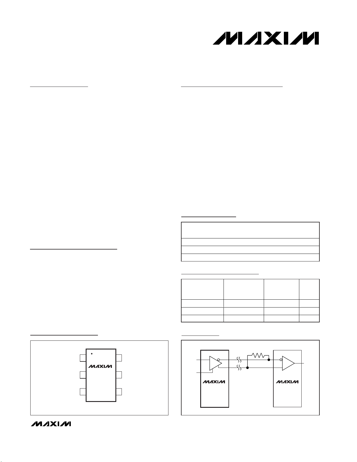
Typical Operating Circuit
MAX3293
MAX3294
MAX3295
D
DI
DE
MAX3280E
MAX3281E
MAX3283E
MAX3284E
R
RO
120Ω
Z
Y
Pin Configuration
MAXIMUM
PART
MAX3293AUT-T 0.25 Yes ABNI
MAX3294AUT-T 2.5 Yes ABNJ
MAX3295AUT-T 20 No ABNK
DATA RATE
(Mbps)
SLEW-RATE
LIMITED
MARK
TOP
TOP VIEW
16Y
DI
V
CC
MAX3293
2
MAX3294
MAX3295
34
SOT23-6
5 GND
ZDE
Page 2
MAX3293/MAX3294/MAX3295
20Mbps, +3.3V, SOT23 RS-485/
RS-422 Transmitters
2 _______________________________________________________________________________________
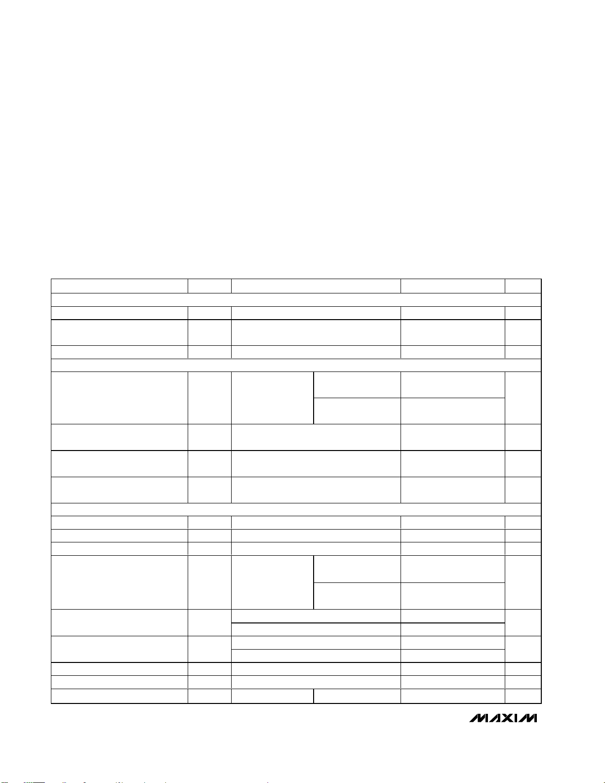
ABSOLUTE MAXIMUM RATINGS
ELECTRICAL CHARACTERISTICS
(VCC= +3.3V ±5%, TA= T
MIN
to T
MAX
, unless otherwise noted. Typical values are at VCC= +3.3V and TA= +25°C.) (Notes 1, 2)
Stresses beyond those listed under “Absolute Maximum Ratings” may cause permanent damage to the device. These are stress ratings only, and functional
operation of the device at these or any other conditions beyond those indicated in the operational sections of the specifications is not implied. Exposure to
absolute maximum rating conditions for extended periods may affect device reliability.
(All voltages referenced to GND, unless otherwise noted.)
Supply Voltage (V
CC
).............................................................+6V
DE, DI .......................................................................-0.3V to +6V
Y, Z .........................................................................-7V to +12.5V
Maximum Continuous Power Dissipation (T
A
= +70°C)
6-Pin SOT23 (derate 6.25mW/°C above +70°C).........500mW
Operating Temperature Ranges
MAX32_ _AUT...............................................-40°C to +125°C
Storage Temperature Range .............................-65°C to +160°C
Junction Temperature .....................................................+160°C
Lead Temperature (soldering, 10s) .................................+300°C
PARAMETER
CONDITIONS
UNITS
POWER SUPPLY
Supply Voltage V
CC
V
Supply Current in Normal
Operation
I
Q
No load, DI = VCC or GND, DE = V
CC
5mA
I
SHDN
No load, DE = GND 1 10 µA
DRIVER
R = 50Ω (RS-422),
T
A
≤ +85°C
2.0
Differential Driver Output V
OD
Figure 1, DE = VCC,
DI = GND or V
CC
R = 27Ω (RS-485),
T
A
≤ +85°C
1.5
V
Change in Magnitude of
Differential Output Voltage
∆V
OD
Figure 1, R = 27Ω or 50Ω,
DE = V
CC
(Note 3)
0.2 V
Driver Common-Mode Output
Voltage
V
OC
Figure 1, R = 27Ω or 50Ω,
DE = V
CC
, DI = VCC or GND
-1 +3 V
Change in Magnitude of CommonMode Voltage
∆V
OC
Figure 1, R = 27Ω or 50Ω (Note 3) 0.2 V
DRIVER LOGIC
Input High Voltage V
IH
DE, DI 2.0 V
Input Low Voltage V
IL
DE, DI 0.8 V
Input Current I
IN
DE, DI -2 +2 µA
VIN = +12V -20
Output Leakage I
O
Y, Z
DE = GND,
V
CC
= GND or
+3.3V
VIN = -7V -20
µA
(VCC - 1V) ≤ V
OUT
≤ +12V, output high
Driver Short-Circuit Foldback
Output Current
I
OSFD
-7V ≤ V
OUT
≤ 1V, output high -25
mA
0 ≤ V
OUT
≤ +12V, output low
Driver Short-Circuit
Output Current
I
OSD
-7V ≤ V
OUT
≤ VCC, output high
mA
Thermal-Shutdown Threshold T
TS
°C
Thermal-Shutdown Hysteresis T
TSH
40 °C
ESD Protection Y, Z Human Body Model ±9 kV
Supply Current in Shutdown Mode
SYMBOL
MIN TYP MAX
3.135 3.300 3.465
V
CC
V
CC
+20
+20
+250
+25
-250
160
Page 3
MAX3293/MAX3294/MAX3295
20Mbps, +3.3V, SOT23 RS-485/
RS-422 Transmitters
_______________________________________________________________________________________ 3
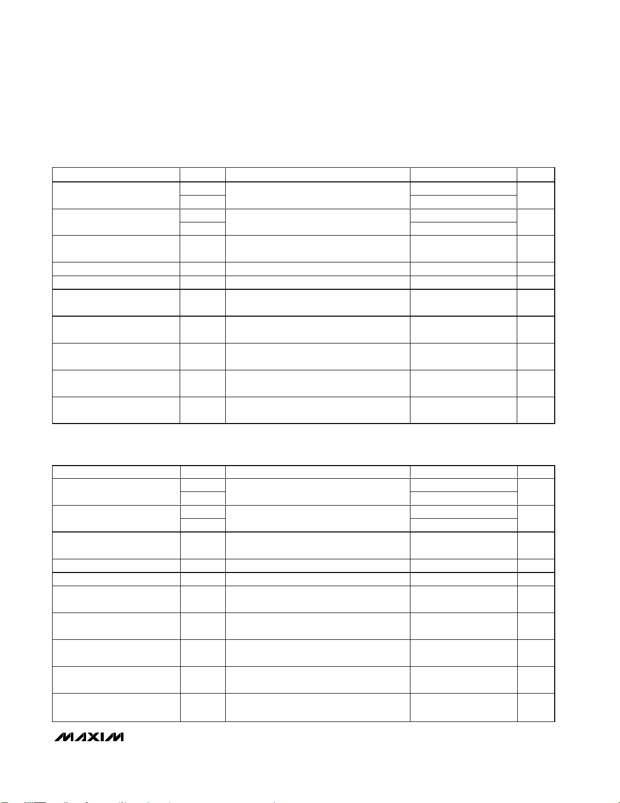
SWITCHING CHARACTERISTICS (MAX3293)
(VCC= +3.3V ±5%, TA= +25°C, unless otherwise noted. Typical values are at VCC= +3.3V.)
SWITCHING CHARACTERISTICS (MAX3294)
(VCC= +3.3V ±5%, TA= +25°C, unless otherwise noted. Typical values are at VCC= +3.3V.)
PARAMETER
CONDITIONS
UNITS
t
PLH
Driver Propagation Delay
t
PHL
Figures 2, 3; R
DIFF
= 54Ω,
C
L
= 50pF
ns
t
R
Driver Differential Output Rise
or Fall Time
t
F
Figures 2, 3; R
DIFF
= 54Ω,
C
L
= 50pF
ns
Driver Output Skew t
SKEW
Figures 2, 3; R
DIFF
= 54Ω, CL = 50pF,
t
SKEW
= | t
PLH
- t
PHL
| (Note 5)
ns
Differential Driver Output Skew
Figures 2, 3; R
DIFF
= 54Ω, CL = 50pF
ns
Maximum Data Rate Figures 2, 3; R
DIFF
= 54Ω, CL = 50pF
kbps
Driver Enable to Output High t
ZH
Figures 4, 5; S2 closed, RL = 500Ω,
C
L
= 100pF
ns
Driver Enable to Output Low t
ZL
Figures 4, 5; S1 closed, RL = 500Ω,
C
L
= 100pF
ns
Driver Disable Time from Low t
LZ
Figures 4, 5; S1 closed, RL = 500Ω,
C
L
= 100pF
ns
Driver Disable Time from High t
HZ
Figures 4, 5; S2 closed, RL = 500Ω,
C
L
= 100pF
ns
Device-to-Device Propagation
Delay Matching
Same power supply, maximum temperature
900 ns
SYMBOL
t
DSKEW
difference between devices = +30°C (Note 5)
MIN TYP MAX
400 1300
400 1300
400 1200
400 1200
-400 +400
-100 +100
250
2000
2000
1000
1000
Driver Propagation Delay
Driver Differential Output Rise
or Fall Time
Driver Output Skew t
Differential Driver Output Skew t
Maximum Data Rate Figures 2, 3; R
Driver Enable to Output High t
Driver Enable to Output Low t
Driver Disable Time from Low t
Driver Disable Time from High t
Device-to-Device Propagation
Delay Matching
PARAMETER SYMBOL CONDITIONS MIN TYP MAX UNITS
t
PLH
t
PHL
t
R
t
F
SKEW
DSKEW
ZH
ZL
LZ
HZ
Figures 2, 3; R
C
= 50pF
L
Figures 2, 3; R
C
= 50pF
L
Figures 2, 3; R
= | t
t
SKEW
Figures 2, 3; R
Figures 4, 5; S2 closed, RL = 500Ω,
= 100pF
C
L
Figures 4, 5; S1 closed, RL = 500Ω,
= 100pF
C
L
Figures 4, 5; S1 closed, RL = 500Ω,
= 100pF
C
L
= 54Ω,
DIFF
= 54Ω,
DIFF
= 54Ω, CL = 50pF,
DIFF
- t
PLH
| (Note 5)
PHL
= 54Ω, CL = 50pF -6 +6 ns
DIFF
= 54Ω, CL = 50pF 2.5 Mbps
DIFF
Figures 4, 5; S2 closed, RL = 500Ω,
= 100pF
C
L
Same power supply, maximum temperature
difference between devices = +30°C (Note 5)
24 70
24 70
10 70
10 70
ns
ns
-40 +40 ns
400 ns
400 ns
100 ns
100 ns
46 ns
Page 4
MAX3293/MAX3294/MAX3295
20Mbps, +3.3V, SOT23 RS-485/
RS-422 Transmitters
4 _______________________________________________________________________________________
Note 1: Devices production tested at +25°C. Limits over the operating temperature range are guaranteed by design.
Note 2: All currents into the device are positive; all currents out of the device are negative. All voltages are referenced to device
ground, unless otherwise noted.
Note 3: ∆V
OD
and ∆VOCare the changes in VODand VOC, respectively, when the DI input changes state.
Note 4: The maximum current applies to peak current just prior to foldback current limiting.
Note 5: Not production tested. Guaranteed by design.
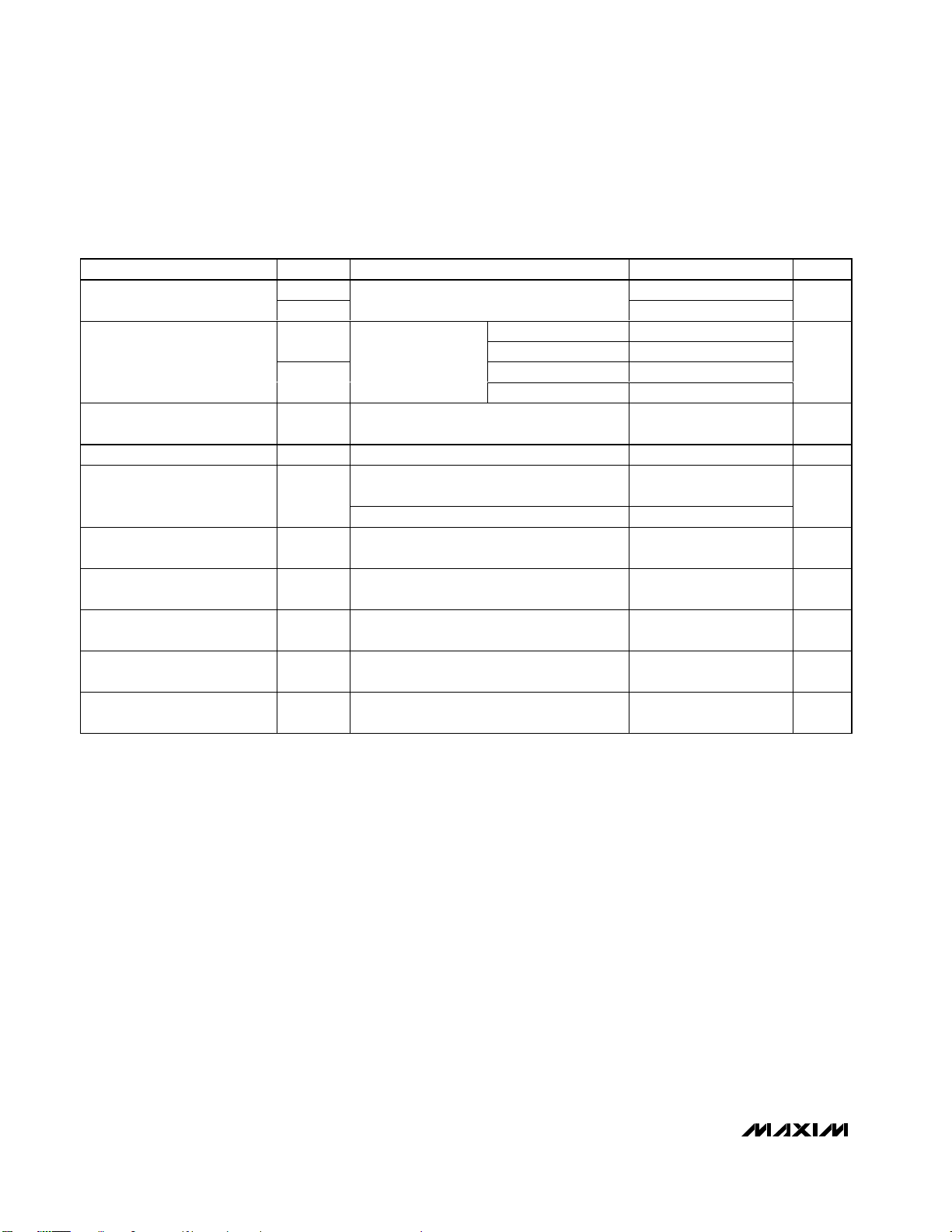
SWITCHING CHARACTERISTICS (MAX3295)
(VCC= +3.3V ±5%, TA= +25°C, unless otherwise noted. Typical values are at VCC= +3.3V.)
PARAMETER
SYMBOL
CONDITIONS
MIN
TYP
MAX
UNITS
t
PLH
25
Driver Propagation Delay
t
PHL
Figures 2, 3; R
DIFF
= 54Ω, CL = 50pF
25
ns
t
R
TA < +85°C 15
Driver Differential Output Rise
or Fall Time
t
F
Figures 2, 3;
R
DIFF
= 54Ω,
C
L
= 50pF
T
A
< +85°C 15
ns
Driver Output Skew t
SKEW
Figures 2, 3; R
DIFF
= 54Ω, CL = 50pF,
t
SKEW
= | t
PLH
- t
PHL
|
5ns
Differential Driver Output Skew
Figures 2, 3; R
DIFF
= 54Ω, CL = 50pF 5 ns
Figures 2, 3; R
DIFF
= 54Ω, CL = 50pF,
T
A
≤ +85°C
20
Maximum Data Rate
Figures 2, 3; R
DIFF
= 54Ω, CL = 50pF 16
Mbps
Driver Enable to Output High t
ZH
Figures 4, 5; S2 closed, RL = 500Ω,
C
L
= 100pF
ns
Driver Enable to Output Low t
ZL
Figures 4, 5; S1 closed, RL = 500Ω,
C
L
= 100pF
ns
Driver Disable Time from Low t
LZ
Figures 4, 5; S1 closed, RL = 500Ω,
C
L
= 100pF
ns
Driver Disable Time from High t
HZ
Figures 4, 5; S2 closed, RL = 500Ω,
C
L
= 100pF
ns
Device-to-Device Propagation
Delay Matching
Same power supply, maximum temperature
25 ns
TA = -40°C to +125°C 18.5
TA = -40°C to +125°C 18.5
t
DSKEW
400
400
difference between devices = +30°C (Note 5)
100
100
Page 5

MAX3293/MAX3294/MAX3295
20Mbps, +3.3V, SOT23 RS-485/
RS-422 Transmitters
_______________________________________________________________________________________ 5
Y
Z
V
OD
R
R
V
OC
Figure 1. Driver DC Test Load
Figure 2. Driver Timing Test Circuit
Figure 3. Driver Propagation Delays
Figure 4. Enable/Disable Timing Test Load
OUTPUT NORMALLY LOW
OUTPUT NORMALLY HIGH
3V
0V
Y, Z
V
OL
Y, Z
0V
1.5V
1.5V
V
OL
+ 0.25V
V
OH
- 0.25V
2.3V
2.3V
t
ZL(SHDN)
, t
ZL
t
LZ
t
ZH(SHDN)
, t
ZH
t
HZ
DE
Figure 5. Driver Enable and Disable Times
Test Circuits and Timing Diagrams
3V
DE
Y
DI
Z
V
S1
OUTPUT
R
L
UNDER TEST
C
L
S2
C
R
V
DIFF
ID
L
C
L
CC
3V
DI
1.5V
0V
Z
V
O
Y
1/2 V
O
V
O
0V
V
DIFF
10%
-V
O
t
R
f = 1MHz, tR ≤ 3ns, tF ≤ 3ns
t
PLH
V
= V (Y) - V (Z)
DIFF
90%
t
= | t
SKEW
PLH
- t
t
PHL
PHL
1.5V
1/2 V
O
90%
t
F
|
10%
Page 6

0
10
20
30
40
MAX3293-95 toc09
TEMPERATURE (°C)
PROPAGATION DELAY (ns)
-40 20 50 80-10 110
DRIVER PROPAGATION DELAY
vs. TEMPERATURE
t
PHL
t
PLH
R
DIFF
= 54Ω
C
L
= 50pF
0
1
2
3
4
OUTPUT SKEW vs. TEMPERATURE
MAX3293-95 toc08
TEMPERATURE (°C)
OUTPUT SKEW (ns)
-40 20 50 80-10 110
DRIVER OUTPUT CURRENT
vs. DRIVER OUTPUT HIGH VOLTAGE
MAX3293-95 toc07
2V/div
OUTPUT HIGH VOLTAGE
OUTPUT CURRENT
(20mA/div)
0mA
-7V 5V
120mA
0
10
30
20
40
50
OUTPUT CURRENT
vs. DIFFERENTIAL OUTPUT VOLTAGE
MAX3293-95 toc04
DIFFERENTIAL OUTPUT VOLTAGE (V)
OUTPUT CURRENT (mA)
1.75 2.752.25 2.502.00 3.00 3.25 3.50
1.0
2.0
2.5
3.0
3.5
MAX3293-95 toc05
TEMPERATURE (°C)
DIFFERENTIAL OUTPUT VOLTAGE (V)
-40 20 50 80-10 110
DRIVER DIFFERENTIAL OUTPUT VOLTAGE
vs. TEMPERATURE
R
DIFF
= 54Ω
R
DIFF
= 100Ω
1.5
DRIVER OUTPUT CURRENT
vs. DRIVER OUTPUT LOW VOLTAGE
MAX3293-95 toc06
2V/div
OUTPUT LOW VOLTAGE
OUTPUT CURRENT
(20mA/div)
0mA
0V 12V
120mA
0
5
10
20
15
25
MAX3295
SUPPLY CURRENT vs. DATA RATE
MAX3293-95 toc01
DATA RATE (Mbps)
SUPPLY CURRENT (mA)
01051520
DE = V
CC
NO LOAD
TA = +85°C
TA = +125°C
TA = +25°C
TA = -40°C
0
0.5
1.0
1.5
2.0
SUPPLY CURRENT vs. TEMPERATURE
MAX3293-95 toc02
TEMPERATURE (°C)
SUPPLY CURRENT (mA)
-40 20 50 80-10 110
DE = V
CC
NO LOAD
NO SWITCHING
0
1.6
1.2
0.8
0.4
2.0
MAX3293-95 toc03
TEMPERATURE (°C)
SUPPLY CURRENT (µA)
-40 20 50 80-10 110
SHUTDOWN SUPPLY CURRENT
vs. TEMPERATURE
DE = GND
MAX3293/MAX3294/MAX3295
20Mbps, +3.3V, SOT23 RS-485/
RS-422 Transmitters
6 _______________________________________________________________________________________
Typical Operating Characteristics
(VCC= +3.3V, TA = +25°C, unless otherwise noted.)
Page 7

DRIVER PROPAGATION DELAY
MAX3293-95 toc10
20ns/div
Y, Z: 1V/div
DI: 2V/div
DI
0V
0V
Y, Z
Typical Operating Characteristics (continued)
(VCC= +3.3V, TA = +25°C, unless otherwise noted.)
MAX3293/MAX3294/MAX3295
20Mbps, +3.3V, SOT23 RS-485/
RS-422 Transmitters
_______________________________________________________________________________________ 7
ENABLE RESPONSE TIME
MAX3293-95 toc11
40ns/div
DE
0V
0V
Y-Z
Y, Z, DE: 2V/div
UNLOADED DRIVER OUTPUT
WAVEFORM (f
IN
= 16Mbps)
MAX3293-95 toc12
20ns/div
Y, Z: 1V/div
0V
Y, Z
LOADED DRIVER OUTPUT WAVEFORM
(f
IN
= 16Mbps)
MAX3293-95 toc13
20ns/div
Y, Z: 500mV/div
0V
Y, Z
EYE DIAGRAM (f
IN
= 20Mbps)
MAX3293-95 toc14
10ns/div
Y, Z: 500mV/div
0V
Y, Z
Pin Description
PIN NAME FUNCTION
1DI
Driver Input. A logic low on DI forces the noninverting output (Y) low and the inverting output (Z)
high. A logic high on DI forces the noninverting output (Y) high and the inverting output (Z) low.
2VCCPositive Supply. VCC = +3.3V ±5%. Bypass VCC to GND with a 0.1µF capacitor.
3DE
Driver Output Enable. Force DE high to enable driver. Pull DE low to disable the driver. Hot-swap
input, see the Hot-Swap Capability section.
4ZInverting RS-485/RS-422 Output
5 GND Ground
6YNoninverting RS-485/RS-422 Output
Page 8
MAX3293/MAX3294/MAX3295
20Mbps, +3.3V, SOT23 RS-485/
RS-422 Transmitters
8 _______________________________________________________________________________________
Detailed Description
The MAX3293/MAX3294/MAX3295 are low-power
transmitters for RS-485/RS-422 communication. The
MAX3295 operates at data rates up to 20Mbps, the
MAX3294 up to 2.5Mbps (slew-rate limited), and the
MAX3293 up to 250kbps (slew-rate limited). These
devices are enabled using an active-high driver enable
(DE) input. When disabled, outputs enter a high-impedance state, and the supply current reduces to 1µA.
The MAX3293/MAX3294/MAX3295 have a hot-swap
input structure that prevents disturbance on the differential signal lines when a circuit board is plugged into
a “hot” backplane (see the Hot-Swap Capability section). Drivers are also short-circuit current limited and
are protected against excessive power dissipation by
thermal-shutdown circuitry.
Driver
The driver accepts a single-ended, logic-level input
(DI) and translates it to a differential RS-485/RS-422
level output (Y and Z). Driving DE high enables the driver, while pulling DE low places the driver outputs
(Y and Z) into a high-impedance state (see Table 1).
Low-Power Shutdown
Force DE low to disable the MAX3293/MAX3294/
MAX3295. In shutdown mode, the device consumes a
maximum of 10µA of supply current.
Hot-Swap Capability
Hot-Swap Input
When circuit boards are inserted into a “hot” or powered backplane, disturbances to the enable can lead to
data errors. Upon initial circuit board insertion, the
processor undergoes its power-up sequence. During
this period, the output drivers are high impedance and
are unable to drive the DE input of the MAX3293/
MAX3294/MAX3295 to a defined logic level. Leakage
currents up to 10µA from the high-impedance output
could cause DE to drift to an incorrect logic state.
Additionally, parasitic circuit board capacitance could
cause coupling of VCCor GND to DE. These factors
could improperly enable the driver.
The MAX3293/MAX3294/MAX3295 eliminate all above
issues with hot-swap circuitry. When VCCrises, an
internal pulldown circuit holds DE low for approximately
10µs. After the initial power-up sequence, the pulldown
circuit becomes transparent, resetting the hot-swap tolerable input.
Table 1. MAX3293/MAX3294/
MAX3295 (RS-485/RS-422) Transmitting
Function Table
X = Don’t care.
INPUTS OUTPUTS
DE DI Y Z
0XShutdown Shutdown
1001
1110
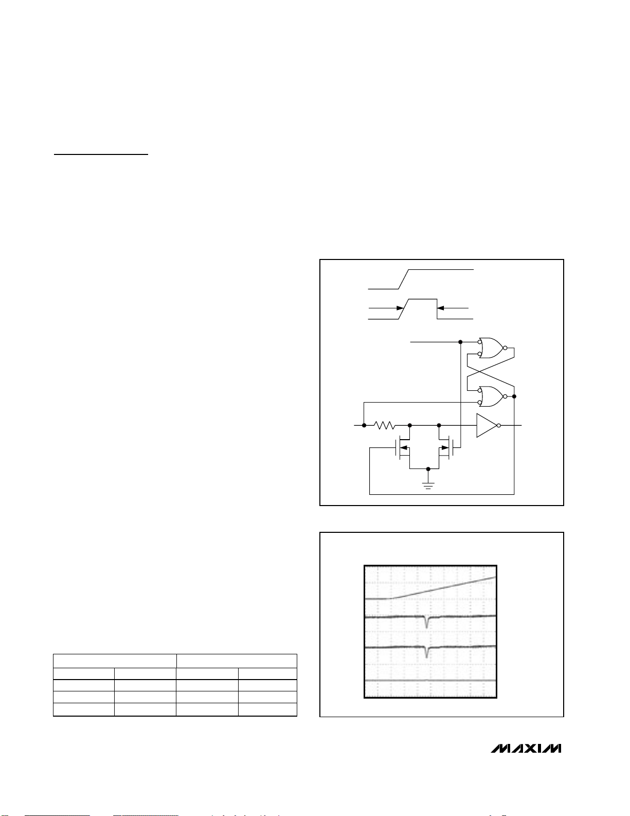
Figure 6. Simplified Structure of the Driver Enable Input (DE)
Figure 7. Differential Power-Up Glitch (0.1V/µs)
DIFFERENTIAL POWER-UP GLITCH
(0.1V/µs)
4µs/div
2V/div
V
CC
Y
Z
Y-Z
0V
10mV/div
AC-COUPLED
10mV/div
AC-COUPLED
20mV/div
EN
V
TIMER
CC
10µs
TIMER
5.6kΩ
100µA
M1 M2
2mA
DE
(HOT SWAP)
Page 9

MAX3293/MAX3294/MAX3295
20Mbps, +3.3V, SOT23 RS-485/
RS-422 Transmitters
_______________________________________________________________________________________ 9
Hot-Swap Input Circuitry
The MAX3293/MAX3294/MAX3295 enable input features hot-swap capability. At the input, there are two
NMOS devices, M1 and M2 (Figure 6). When V
CC
ramps from zero, an internal 10µs timer turns on M2
and sets the SR latch, which also turns on M1.
Transistors M2, a 2mA current sink, and M1, a 100µA
current sink, pull DE to GND through a 5.6kΩ resistor.
M2 is designed to pull DE to the disabled state against
an external parasitic capacitance up to 100pF that may
drive DE high. After 10µs, the timer deactivates M2
while M1 remains on, holding DE low against threestate leakages that can drive DE high. M1 remains on
until an external source overcomes the required input
current. At this time, the SR latch resets and M1 turns
off. When M1 turns off, DE reverts to a standard, highimpedance CMOS input. Whenever VCCdrops below
1V, the hot-swap input is reset.
Hot-Swap Line Transient
During a hot-swap event when the driver is connected to
the line and is powered up, the driver must not cause the
differential signal to drop below 200mV. Figures 7, 8, and
9 show the results of the MAX3295 during power-up for
three different VCCramp rates (0.1V/µs, 1V/µs, and
10V/µs). The photos show the VCCramp, the singleended signal on each side of the 100Ω termination, as
well as the differential signal across the termination.
ESD Protection
Human Body Model
Figure 10 shows the Human Body Model, and Figure 11
shows the current waveform it generates when discharged into low impedance. This model consists of a
100pF capacitor charged to the ESD voltage of interest,
which is then discharged into the device through a
1.5kΩ resistor.
Figure 8. Differential Power-Up Glitch (1V/µs)
Figure 9. Differential Power-Up Glitch (10V/µs) Figure 11. Current Waveform
DIFFERENTIAL POWER-UP GLITCH
(10V/µs)
200ns/div
2V/div
V
CC
Y
Z
Y-Z
0V
50mV/div
AC-COUPLED
50mV/div
AC-COUPLED
100mV/div
Figure 10. Human Body ESD Test
CHARGE-CURRENT-
LIMIT RESISTOR
DISCHARGE
RESISTANCE
STORAGE
CAPACITOR
C
s
100pF
R
C
1MΩ
R
D
1.5kΩ
HIGH-
VOLTAGE
DC
SOURCE
DEVICE
UNDER
TEST
DIFFERENTIAL POWER-UP GLITCH
(1V/µs)
V
CC
Y
Z
2V/div
0V
100mV/div
AC-COUPLED
100mV/div
AC-COUPLED
Y-Z
1µs/div
200mV/div
IP 100%
90%
AMPERES
36.8%
10%
0V
0V
I
r
PEAK-TO-PEAK RINGING
(NOT DRAWN TO SCALE)
TIME
t
RL
t
DL
CURRENT WAVEFORM
Page 10

Reduced EMI and Reflections
(MAX3293/MAX3294)
The MAX3293/MAX3294 are slew-rate limited, minimizing EMI and reducing reflections caused by improperly
terminated cables. Figure 12 shows Fourier analysis of
the MAX3295 transmitting a 125kHz signal. High-frequency harmonics with large amplitudes are evident.
Figure 13 shows the same information, but for the slewrate-limited MAX3293, transmitting the same signal.
The high-frequency harmonics have much lower amplitudes, and the potential for EMI is significantly reduced.
To minimize reflections, the line should be terminated at
both ends in its characteristic impedance, and stub
lengths off the main line should be kept as short as
possible. The slew-rate-limited MAX3293 and MAX3294
are more tolerant of imperfect termination.
Driver Output Protection
Two mechanisms prevent excessive output current and
power dissipation caused by faults or by bus contention.
The first, a foldback current limit on the output stage,
provides immediate protection against short circuits over
the whole common-mode voltage range (see the Typical
Operating Characteristics). The second, a thermal-shutdown circuit, forces the driver outputs into a high-impedance state if the die temperature exceeds +160°C.
MAX3293/MAX3294/MAX3295
20Mbps, +3.3V, SOT23 RS-485/
RS-422 Transmitters
10 ______________________________________________________________________________________
Figure 12. Driver Output Waveform and FFT Plot of MAX3295
Transmitting a 125kHz Signal
Figure 13. Driver Output Waveform and FFT Plot of MAX3293
Transmitting a 125kHz Signal
DRIVER OUTPUT WAVEFORM AND
FFT PLOT OF MAX3293
10dB/div
Chip Information
TRANSISTOR COUNT: 263
PROCESS: BiCMOS
DRIVER OUTPUT WAVEFORM AND
FFT PLOT OF MAX3295
10dB/div
Page 11

MAX3293/MAX3294/MAX3295
20Mbps, +3.3V, SOT23 RS-485/
RS-422 Transmitters
Maxim cannot assume responsibility for use of any circuitry other than circuitry entirely embodied in a Maxim product. No circuit patent licenses are
implied. Maxim reserves the right to change the circuitry and specifications without notice at any time.
Maxim Integrated Products, 120 San Gabriel Drive, Sunnyvale, CA 94086 408-737-7600 ____________________ 11
© 2004 Maxim Integrated Products Printed USA is a registered trademark of Maxim Integrated Products.
Package Information
(The package drawing(s) in this data sheet may not reflect the most current specifications. For the latest package outline information
go to www.maxim-ic.com/packages
.)
6LSOT.EPS
F
1
1
21-0058
PACKAGE OUTLINE, SOT-23, 6L
 Loading...