

MAX3291/MAX3292
RS-485/RS-422 Transceivers with Preemphasis
for High-Speed, Long-Distance Communication
________________________________________________________________
Maxim Integrated Products
1
19-1405; Rev 1; 4/99
For free samples & the latest literature: http://www.maxim-ic.com, or phone 1-800-998-8800.
For small orders, phone 1-800-835-8769.
________________General Description
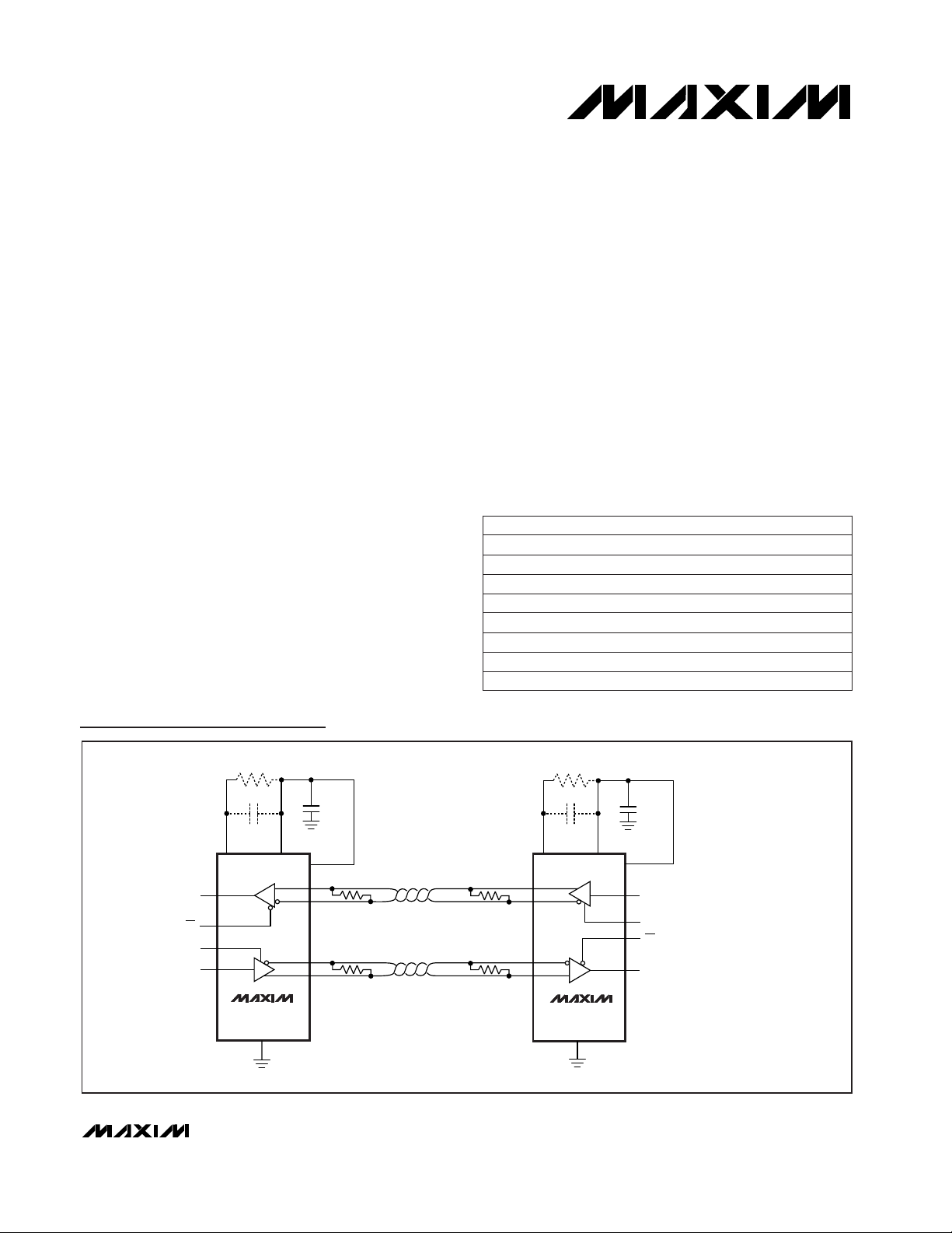
The MAX3291/MAX3292 high-speed RS-485/RS-422
transceivers feature driver preemphasis circuitry, which
extends the distance and increases the data rate of reliable communication by reducing intersymbol interference (ISI) caused by long cables. The MAX3291 is
programmable for data rates of 5Mbps to 10Mbps,
while the MAX3292 is programmable for data rates up
to 10Mbps by using a single external resistor.
The MAX3291/MAX3292 are full-duplex devices that
operate from a single +5V supply and offer a low-current shutdown mode that reduces supply current to
100nA. They feature driver output short-circuit current
limiting and a fail-safe receiver input that guarantees a
logic-high output if the input is open circuit. A 1/4-unitload receiver input impedance allows up to 128 transceivers on the bus.
________________________Applications
Long-Distance, High-Speed RS-485/RS-422
Communications
Telecommunications
Industrial-Control Local Area Networks
____________________________Features
♦ Preemphasis Increases the Distance and Data
Rate of Reliable RS-485/RS-422 Communication
♦ Data Rate
Optimized for 5Mbps to 10Mbps (MAX3291)
Programmable up to 10Mbps (MAX3292)
♦ 100nA Low-Current Shutdown Mode
♦ Allow Up to 128 Transceivers on the Bus
♦ -7V to +12V Common-Mode Input Voltage Range
♦ Pin-Compatible with ’75180, MAX489, MAX491
MAX3080, MAX3083, MAX3086, MAX1482
2
PEE
(PSET)
12
13
R = Z
O
R = Z
O
R = Z
O
R = Z
O
14
1
1µF
R
PSET
*
C
PSET
*C
PSET
*
7(6)
GND
11
10
9
( ) ARE FOR MAX3292
* MAX3292 ONLY
Z
O
= THE CHARACTERISTIC
IMPEDANCE OF THE CABLE
RO
RE
DE
DI
3
4
5
9
5
13
7(6)
GND
4
3
DI
DE
RE
RO
2
10
11
12
V
CC
(V
CCD
)(V
CCD
)
PEE
(PSET)
14
1
1µF
R
PSET
*
V
CC
MAX3291
MAX3292
MAX3291
MAX3292
A
B
Z
Y
Y
Z
B
A
Typical Operating Circuit and Functional Diagram
PART
MAX3291CSD
MAX3291CPD
MAX3291ESD -40°C to +85°C
0°C to +70°C
0°C to +70°C
TEMP. RANGE PIN-PACKAGE
14 SO
14 Plastic DIP
14 SO
_______________Ordering Information
MAX3291EPD -40°C to +85°C 14 Plastic DIP
MAX3292CSD
MAX3292CPD
MAX3292ESD -40°C to +85°C
0°C to +70°C
0°C to +70°C 14 SO
14 Plastic DIP
14 SO
MAX3292EPD -40°C to +85°C 14 Plastic DIP
Pin Configuration appears at end of data sheet.
MAX3291/MAX3292
RS-485/RS-422 Transceivers with Preemphasis
for High-Speed, Long-Distance Communication
2 _______________________________________________________________________________________
ABSOLUTE MAXIMUM RATINGS
DC ELECTRICAL CHARACTERISTICS
(Typical Operating Circuit, VCC= +5V ±5%, R
PSET
= 0 (MAX3292), VCC= V
CCD
(MAX3292), TA= T
MIN
to T
MAX
, unless otherwise
noted. Typical values are at V
CC
= +5V and TA= +25°C.) (Note 1)
Stresses beyond those listed under “Absolute Maximum Ratings” may cause permanent damage to the device. These are stress ratings only, and functional
operation of the device at these or any other conditions beyond those indicated in the operational sections of the specifications is not implied. Exposure to
absolute maximum rating conditions for extended periods may affect device reliability.
Supply Voltage (VCC, V
CCD
) .................................................+6V
Control Input Voltage (
RE, DE, PEE,
PSET, DI).................................................-0.3V to (V
CC
+ 0.3V)
Driver Output Voltage (Y, Z)................................-7.5V to +12.5V
Receiver Input Voltage (A, B)..............................-7.5V to +12.5V
Receiver Output Voltage (RO)....................-0.3V to (V
CC
+ 0.3V)
Continuous Power Dissipation (T
A
= +70°C)
14-Pin SO (derate 8.7mW/°C above +70°C).................695mW
14-Pin Plastic DIP (derate 10.0mW/°C above +70°C) ..800mW
Operating Temperature Ranges
MAX329_C_ D......................................................0°C to +70°C
MAX329_E_ D...................................................-40°C to +85°C
Storage Temperature Range.............................-65°C to +160°C
Lead Temperature (soldering, 10sec).............................+300°C
R = 27Ω
DE = GND,
VCC= GND or 5.25V
V
PSET
= V
CC
DE, DI, RE
DE, DI, RE, PEE
DE, DI, RE
CONDITIONS
V2.4V
ODP
Differential Driver Output with
Preemphasis
µA
-25
I
O
Output Leakage (Y and Z)
25
µA70 110I
PSET
PSET Input Current (MAX3292)
V
2.4
V
IH
Input High Voltage
V0.8V
IL
Input Low Voltage
µA±2I
IN
Input Current
µA-15 -30 -45I
PEE
PEE Input Current (MAX3291)
UNITSMIN TYP MAXSYMBOLPARAMETER
Figure 1, R = 27Ω (Note 3) V1.65 2.0 2.35DPER
Differential Driver
Preemphasis Ratio
Figure 1, R = 27Ω (Note 4) V0.2
∆VOD,
∆V
ODP
Change in Magnitude of
Differential Output Voltage
(Normal and Preemphasis)
Figure 1, R = 27Ω VV
CC
/ 2 3V
OC
Driver Common-Mode Output
Voltage (Normal and
Preemphasis)
Figure 1, R = 27Ω (Note 5) V0.3∆V
OC
Change in Magnitude of
Common-Mode Voltage
(Normal and Preemphasis)
Figure 1, R = 27Ω mV50∆V
NP
Change in Magnitude of
Common-Mode Output
Voltage (Normal to
Preemphasis)
-7V ≤ V
OUT
≤ +12V (Note 6) mA±30 ±250I
OSD
Driver Short-Circuit Output
Current
VY= VZ= +12V
VY= VZ= -7V
R = 27Ω
Figure 1
No load (Note 2)
V
5.25
V
OD
1.5 5.0
Differential Driver Output
PEE 3.75
DRIVER
MAX3291/MAX3292
RS-485/RS-422 Transceivers with Preemphasis
for High-Speed, Long-Distance Communication
_______________________________________________________________________________________ 3
DC ELECTRICAL CHARACTERISTICS (continued)
(Typical Operating Circuit, VCC= +5V ±5%, R
PSET
= 0 (MAX3292), V
CC
= V
CCD
(MAX3292), TA= T
MIN
to T
MAX
, unless otherwise
noted. Typical values are at V
CC
= +5V and TA= +25°C.) (Note 1)
SWITCHING CHARACTERISTICS
(Typical Operating Circuit, VCC= +5V ±5%, R
PSET
= 0 (MAX3292), VCC= V
CCD
(MAX3292), TA= +25°C, unless otherwise noted.
Typical values are at V
CC
= +5V and TA= +25°C.)
-7V ≤ VCM≤ +12V
RE = V
CC,
DE = GND, VY= VZ= 0 to VCCor
floating
RE = GND, DE = V
CC
0 ≤ VO≤ V
CC
-7V ≤ VCM≤ +12V
0 ≤ VRO≤ V
CC
CONDITIONS
mV-200 200V
TH
Receiver Differential
Threshold Voltage
µA0.1 1I
SHDN
Supply Current in Shutdown
Mode
mA2.0 3.0I
CC + ICCD
No-Load Supply Current
µA0.1 ±1I
OZR
Three-State Output Current at
Receiver
kΩ48R
IN
Receiver Input Resistance
mA±15 ±95I
OSR
Receiver Output Short-Circuit
Current
UNITSMIN TYP MAXSYMBOLPARAMETER
VA= VB= 0 mV35∆V
TH
Receiver Input Hysteresis
IO= -4mA, VA- VB= V
TH
V3.5V
OH
Receiver Output High Voltage
IO= 4mA, VA- VB= -V
TH
V0.4V
OL
Receiver Output Low Voltage
DE = GND,
VCC= GND or 5.25V
µA
-150
IA,
B
250
Input Current (A and B)
VIN= +12V
VIN= -7V
Driver Differential Output
Rise or Fall Time
Figures 3 and 5, R
DIFF
= 54Ω,
CL1= CL2= 50pF
ns
44 65t
DPHL
Driver Propagation Delay
CONDITIONS
t
HL
12
Figures 3 and 5, R
DIFF
= 54Ω,
CL1= CL2= 50pF
ns
t
LH
Differential Driver Output
Skew t
DPLH
- t
DPHL
Figures 3 and 10, R
DIFF
= 54Ω,
CL1= CL2= 50pF
ns30t
PTND
Preemphasis Voltage Level to
Normal Voltage Level Delay
t
DSKEW
Figures 3 and 5, R
DIFF
= 54Ω,
CL1= CL2= 50pF
38ns
Mbps10f
MAX
Maximum Data Rate
41 65t
DPLH
UNITSMIN TYP MAXSYMBOLPARAMETER
RECEIVER
SUPPLY CURRENT
Driver Preemphasis Interval t
PRE
80 100 120
Figures 3 and 10,
R
DIFF
= 54Ω,
C
L1
= CL2= 50pF
ns
0.75 1 1.25 µs
MAX3292,
R
PSET
= 523kΩ
MAX3291/MAX3292,
R
PSET
= 0

MAX3291/MAX3292
RS-485/RS-422 Transceivers with Preemphasis
for High-Speed, Long-Distance Communication
4 _______________________________________________________________________________________
SWITCHING CHARACTERISTICS (continued)
(Typical Operating Circuit, VCC= +5V ±5%, R
PSET
= 0 (MAX3292), VCC= V
CCD
(MAX3292), TA= +25°C, unless otherwise noted.
Typical values are at V
CC
= +5V and TA= +25°C.)
Note 1: All currents into the device are positive; all currents out of the device are negative. All voltages are referenced to device
ground unless otherwise noted.
Note 2: Guaranteed by design.
Note 3: DPER is defined as (V
ODP
/ VOD).
Note 4: ∆V
ODP
and ∆VOCare the changes in VDDand VOC, respectively, when the DI input changes. This specification reflects
constant operating conditions. When operating conditions shift, the maximum value may be momentarily exceeded.
Note 5: ∆V
ODP
and ∆VOCare the changes in VODand VOC, respectively, when the DI input changes state.
Note 6: Maximum current level applies to peak current just prior to foldback-current limiting; minimum current level applies during
current limiting.
Note 7: Shutdown is enabled by bringing RE high and DE low. If the enable inputs are in this state for less than 50ns, the device is
guaranteed not to enter shutdown. If the enable inputs are in this state for at least 500ns, the device is guaranteed to have
entered shutdown. Time to shutdown for the device (t
SHDN
) is measured by monitoring R0 as in Figure 4.
Figures 2 and 6, S2 closed, RL= 500Ω,
C
L
= 100pF
Figures 2 and 6, RL= 500Ω, CL= 100pF,
S2 closed
CONDITIONS
ns
ns6000 8750t
DZH(SHDN)
Driver Enable from Shutdown
to Output High
UNITSMIN TYP MAXSYMBOLPARAMETER
Figures 4 and 11 (Note 7) ns50 160 500t
SHDN
Time to Shutdown
Figures 2 and 8, RL= 1kΩ, CL= 100pF,
S1 closed
ns34355t
RZL
Receiver Enable to Output
Low
Figures 2 and 8, RL= 1kΩ, CL= 15pF,
S1 closed
ns
Figures 2 and 8, RL= 1kΩ, CL= 100pF,
S2 closed
25 45t
RLZ
Receiver Disable Time from
Low
ns34355t
RZH
Receiver Enable to Output
High
Figures 2 and 8, RL= 1kΩ, CL= 15pF,
S2 closed
ns25 45t
RHZ
Receiver Disable Time from
High
Figures 2 and 6, RL= 500Ω, CL= 100pF,
S1 closed
ns6000 8750t
DZL(SHDN)
Driver Enable from Shutdown
to Output Low
Figures 2 and 8, RL= 1kΩ, CL= 100pF,
S1 closed
ns30 1500t
RZL(SHDN)
Receiver Enable from
Shutdown to Output Low
Figures 2 and 8, RL= 1kΩ, CL= 100pF,
S2 closed
ns850 1500t
RZH(SHDN)
Receiver Enable from
Shutdown to Output High
Figures 7 and 9, CL= 100pF ns3t
RSKEW
Receiver Output Skew
t
RPLH
- t
RPHL
Driver Enable to Output High t
DZH
72 105
Figures 7 and 9, CL= 50pF, VID= 2V,
VCM= 0
Receiver Propagation Delay
t
RPHL
52 85
ns
49 85t
RPLH
Figures 2 and 6, S2 closed, RL= 500Ω,
C
L
= 15pF
Driver Disable Time from High t
DHZ
71 100 ns
Figures 2 and 6, S1 closed, RL= 500Ω,
C
L
= 15pF
Driver Disable Time from Low t
DLZ
53 100 ns
Figures 2 and 6, S1 closed, RL= 500Ω,
C
L
= 100pF
Driver Enable to Output Low t
DZL
55 105 ns
MAX3291/MAX3292
RS-485/RS-422 Transceivers with Preemphasis
for High-Speed, Long-Distance Communication
_______________________________________________________________________________________
5
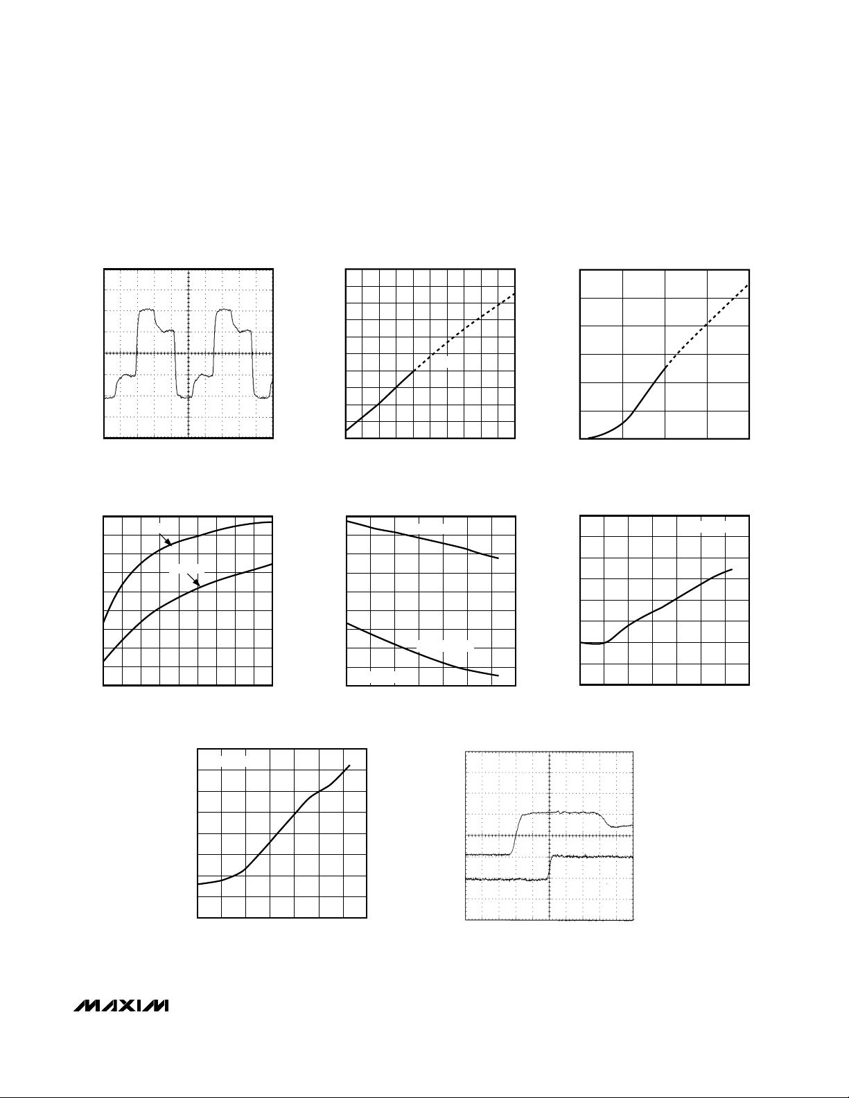
TYPICAL PREEMPHASIS WAVEFORM
MAX3291/2-01
100ns/div
V
Y
- V
Z
2V/
div
2500
0
0 1000
PREEMPHASIS INTERVAL vs. R
PSET
(C
PSET
= 0.1µF)
250
500
2250
MAX3291/2-02
R
PSET
(kΩ)
PREEMPHASIS INTERVAL (ns)
200100 300 400 600500
800
700 900
2000
1750
750
1500
1250
1000
NOTE A
0
400
200
800
NOTE A
600
1000
1200
0 1000500 1500 2000
R
PRE
AND t
PRE
vs. t
BAUD
MAX3291/92 toc 03
t
BAUD
(ns)
R
PRE
(kΩ)
0
1.0
0.5
2.0
1.5
2.5
3.0
4.0
3.5
4.5
10 30 40 5020 60 70 80 90
100
DRIVER DIFFERENTIAL
OUTPUT VOLTAGE vs. R
DIFF
MAX3291/2-04
R
DIFF
(Ω)
DRIVER DIFFERENTIAL OUTPUT VOLTAGE (V)
STRONG
NORMAL
30.0
35.0
32.5
40.0
37.5
42.5
47.5
45.0
50.0
-40 0 20-20 40 60 80
100
DRIVER PROPAGATION DELAY
vs. TEMPERATURE
MAX3291/2-07
TEMPERATURE (°C)
PROPAGATION DELAY (ns)
C
L1
= C
L2
= 50pF
2.00
2.50
2.25
3.00
2.75
3.25
3.50
4.00
3.75
4.25
-40 0 20-20 40 60 80
100
DRIVER DIFFERENTIAL
OUTPUT VOLTAGE vs. TEMPERATURE
MAX3291/2-05
TEMPERATURE (°C)
DIFFERENTIAL OUTPUT VOLTAGE (V)
STRONG (V
ODP
)
R
DIFF
= 54Ω
NORMAL (VOD)
40.0
45.0
42.5
50.0
47.5
52.5
57.5
55.0
60.0
-40 0 20-20 40 60 80
100
RECEIVER PROPAGATION DELAY
vs. TEMPERATURE
MAX3291/2-06
TEMPERATURE (°C)
PROPAGATION DELAY (ns)
CL = 50pF
RECEIVER PROPAGATION DELAY
MAX3291/2-08
20ns/div
V
A
- V
B
RO
2.5V/
div
5V/
div
__________________________________________Typical Operating Characteristics
(VCC= +5V, TA= +25°C, unless otherwise noted.)
Note A: Dotted line represents region in which preemphasis may not work in systems with excessive power-supply noise. See
Preemphasis at Low Data Rates
.

MAX3291/MAX3292
RS-485/RS-422 Transceivers with Preemphasis
for High-Speed, Long-Distance Communication
6 _______________________________________________________________________________________
____________________________________Typical Operating Characteristics (continued)
(VCC= +5V, TA= +25°C, unless otherwise noted.)
0
0.75
0.50
0.25
1.75
1.50
1.25
1.00
2.00
2.75
2.50
2.25
3.00
-40 0 20-20 40 60 80
100
NO-LOAD SUPPLY CURRENT
vs. TEMPERATURE
MAX3291/2-12
TEMPERATURE (°C)
NO-LOAD SUPPLY CURRENT (mA)
0
20
10
40
30
60
50
70
0 1.0 1.50.5 2.0 2.5 3.0 3.5 4.0 4.5 5.0
OUTPUT SINK CURRENT vs.
RECEIVER OUTPUT LOW VOLTAGE
MAX3291/2-13
OUTPUT LOW VOLTAGE (V)
OUTPUT SINK CURRENT (mA)
0
0.10
0.05
0.15
0.20
0.25
0.30
-40 0 20-20 40 60 80
100
RECEIVER OUTPUT LOW VOLTAGE
vs. TEMPERATURE
MAX3291/2-10
TEMPERATURE (°C)
OUTPUT LOW VOLTAGE (V)
IRO = 8mA
0
5
15
10
25
20
30
0 1.0 1.50.5 2.0 2.5 3.0 3.5 4.0 4.5 5.0
OUTPUT SOURCE CURRENT vs.
RECEIVER OUTPUT HIGH VOLTAGE
MAX3291/2-14
OUTPUT HIGH VOLTAGE (V)
OUTPUT SOURCE CURRENT (mA)
4.10
4.25
4.20
4.15
4.35
4.30
4.45
4.40
4.55
4.50
4.60
-40 0 20-20 40 60 80
100
RECEIVER OUTPUT HIGH VOLTAGE
vs. TEMPERATURE
MAX3291/2-11
TEMPERATURE (°C)
OUTPUT HIGH VOLTAGE (V)
IRO = 8mA
DRIVER PROPAGATION DELAY
MAX3291/2-09
20ns/div
V
Y
- V
Z
DI
2.5V/
div
5V/
div

MAX3291/MAX3292
RS-485/RS-422 Transceivers with Preemphasis
for High-Speed, Long-Distance Communication
_______________________________________________________________________________________ 7
Pin Description
Preemphasis Enable Input. To enable preemphasis, leave PEE unconnected, connect to
VCC, or drive high. To enable strong-level-drive only mode, connect PEE to GND or drive
low.
PEE1 —
Preemphasis Set Input. Sets the preemphasis interval. Connect a resistor (R
PSET
) in paral-
lel with a capacitor (C
PSET
) from PSET to VCCto set the preemphasis interval. See
Typical
Operating Circuit
.
PSET— 1
Receiver Output Enable. Drive RE low to enable RO; RO is high impedance when RE is
high. Drive RE high and DE low to enter low-power shutdown mode.
RE
3 3
Receiver Output. When RE is low and if A - B ≥ 200mV, RO is high; if A - B ≤ -200mV, RO
is low.
RO2 2
Driver Input. With DE high, a low on DI forces the noninverting output low and the inverting
output high. Similarly, a high on DI forces the noninverting output high and the inverting
output low.
DI5 5
GroundGND7 6, 7
No Connection. Not internally connected.N.C.6, 8, 13 8
Driver Output Enable. Drive DE high to enable the driver outputs. These outputs are high
impedance when DE is low. Drive RE high and DE low to enter low-power shutdown mode.
DE4 4
Noninverting Driver OutputY9 9
Inverting Receiver InputB11 11
Connect to V
CC
V
CCD
— 13
Noninverting Receiver InputA12 12
Inverting Driver OutputZ10 10
PIN
MAX3291
FUNCTIONNAME
MAX3292
Figure 1. Driver DC Test Load
OUTPUT
UNDER TEST
R
L
S1
S2
V
CC
C
L
Figure 2. Driver or Receiver Enable/Disable Timing Test Load
Positive Supply: +4.75V ≤ VCC≤ +5.25VV
CC
14 14
Y
Z
R
V
OD
V
ODP
R
V
OC

MAX3291/MAX3292
RS-485/RS-422 Transceivers with Preemphasis
for High-Speed, Long-Distance Communication
8 _______________________________________________________________________________________
DI
DE
D
5V
Y
Z
C
L1
C
L2
R
DIFF
V
ODP
Figure 3. Driver Timing Test Circuit Figure 4. Shutdown Timing Diagram
DI
5V
0
Z
N
Y
P
Z
P
Y
N
Z
N
Z
P
Y
P
Y
N
0 DIFFERENTIAL
0 DIFFERENTIAL
1.5V
t
DPLH
20%
80%
80%
t
DPHL
1.5V
20%
t
HL
t
LH
V
DIFF
= VY - V
Z
V
DIFF
t
SKEW = | tPLH
- t
PHL
|
|
YN - ZN | = V
OD
|
YP - ZP | = V
ODP
Figure 5. Driver Propagation Delays Figure 6. Driver Enable and Disable Times
RO
V
OH
V
OL
A
+1V
B
-1V
0 DIFFERENTIAL
1.5V
t
RPHL
t
RPLH
1.5V
t
RSKEW = | tRPLH
- t
RPHL
|
Figure 7. Receiver Propagation Delays Figure 8. Receiver Enable and Disable Times
t < t
SHDN
RE
RO
DE = LOW
5V
DE
1.5V
0
t
Y, Z
DZL(SHDN)
2.3V
Y, Z
0
2.3V
t
DZH(SHDN)
t > t
SHDN
, t
DZL
t
DLZ
OUTPUT NORMALLY LOW
OUTPUT NORMALLY HIGH
, t
DZH
t
DHZ
t
RZH(SHDN)
1.5V
VOL* + 0.5V
V
OH
* - 0.5V
V
PH
V
PL
*NOTE: V
S2 AND S1 CLOSED, RESPECTIVELY.
AND VOL ARE THE OUTPUT LEVELS IN FIGURE 2 WITH
OH
3V
RE
V
CC
RO
RO
1.5V 1.5V
0
, t
t
RZL(SHDN)
1.5V
OUTPUT NORMALLY LOW
OUTPUT NORMALLY HIGH
1.5V
0
t
, t
RZH(SHDN)
RZL
RZH
t
RLZ
V
+ 0.5V
OL
V
- 0.5V
OH
t
RHZ

INPUTS
MAX3291/MAX3292
RS-485/RS-422 Transceivers with Preemphasis
for High-Speed, Long-Distance Communication
_______________________________________________________________________________________ 9
R
B
RO
C
L
ATE
A
V
ID
R
Figure 9. Receiver Propagation Delay Test Circuit Figure 10. Preemphasis Timing
RE
DI
DE
1k
V
CC
RO
MAX3291
MAX3292
Figure 11. Time-to-Shutdown Test Circuit
Function Tables
DI
RE
DE
1X 1
INPUTS
Z
0
OUTPUTS
Y
1
TRANSMITTING
1 00X 1
High-Z High-Z
High-Z and
SHUTDOWN
X1 0
X0 0
A-B
RE
DE
OUTPUT
RO
1
0≤ -0.2V0 X
1
High-Z and
SHUTDOWN
X1 0
Open0 X
≥ 0.2V0 X
X = Don’t care
Z = High impedance
SHUTDOWN = Low-power shutdown; driver and receiver outputs are high impedance.
INPUTS
RECEIVING
High-ZX1 1
t
PTND
Y
P
Z
N
0 DIFFERENTIAL
Y
N
80%
20%
50%
Z
P
t
PRE
Z
P
Y
N
Z
N
Y
P

MAX3291/MAX3292
Detailed Description
The MAX3291/MAX3292 high-speed RS-485/RS-422
transceivers feature driver preemphasis circuitry, which
extends the distance and increases the data rate of
reliable communication by reducing intersymbol interference (ISI) caused by long cables. The MAX3291 is
programmable for data rates of 5Mbps to 10Mbps,
while the MAX3292 is programmable for data rates up
to 10Mbps by using a single external resistor.
The MAX3291/MAX3292 are full-duplex devices that
operate from a single +5V supply and offer a low-current shutdown mode that reduces supply current to
100nA. They feature driver output short-circuit current
limiting and a fail-safe receiver input that guarantees a
logic-high output if the input is open circuit. A 1/4-unitload receiver input impedance allows up to 128 transceivers on the bus.
Inter-symbol interference (ISI) causes significant problems for UARTs if the total RS-485/RS-422 signal jitter
becomes 10% or more of the baud period. ISI is
caused by the effect of the cable’s RC time constant on
different bit patterns. If a series of ones is transmitted,
followed by a zero, the transmission-line voltage rises
to a high value at the end of the string of ones (signal 1
in Figure 12). As the signal moves towards the zero
state, it takes longer to reach the zero-crossing,
because its starting voltage is farther from the zero
crossing. On the other hand, if the data pattern has a
string of zeros followed by a one and then another zero,
the one-to-zero transition starts from a voltage that is
much closer to the zero-crossing (VA- VB= 0) and it
takes much less time for the signal to reach the zerocrossing (signal 2 in Figure 12). In other words, the
propagation delay depends upon the previous bit pattern. This is inter-symbol interference (ISI).
Preemphasis reduces ISI by increasing the signal
amplitude at every transition edge for about one baud
period, counteracting the effects of the cable (see the
section
Setting the Preemphasis Interval
). Figure 13
shows a typical preemphasis waveform optimized for
data rates between 5Mbps and 10Mbps. When DI
changes from a logic low to a logic high, the differential
output switches to a strong high. At the end of the preemphasis interval, the strong high returns to a normal
high level. Both levels meet RS-485/RS-422 specifications, and the strong levels are typically 1.9 times larger
than the normal levels. If DI switches back to a logic
low before the end of the preemphasis interval, the differential output switches directly from the strong high to
the strong low. Similarly, this explanation applies when
DI transitions from high to low.
Applications Information
Data Rate vs. Cable Length
In general, preemphasis allows either double the distance for a fixed data rate or double the data rate for a
fixed existing cable distance over existing RS-485
transceivers that do not feature preemphasis. Figure 14
shows that the MAX3291/MAX3292 transmits approximately twice as far at the same data rate or twice as
fast at the same cable length as a conventional RS-485
transceiver without preemphasis for 10% jitter.
RS-485/RS-422 Transceivers with Preemphasis
for High-Speed, Long-Distance Communication
10 ______________________________________________________________________________________
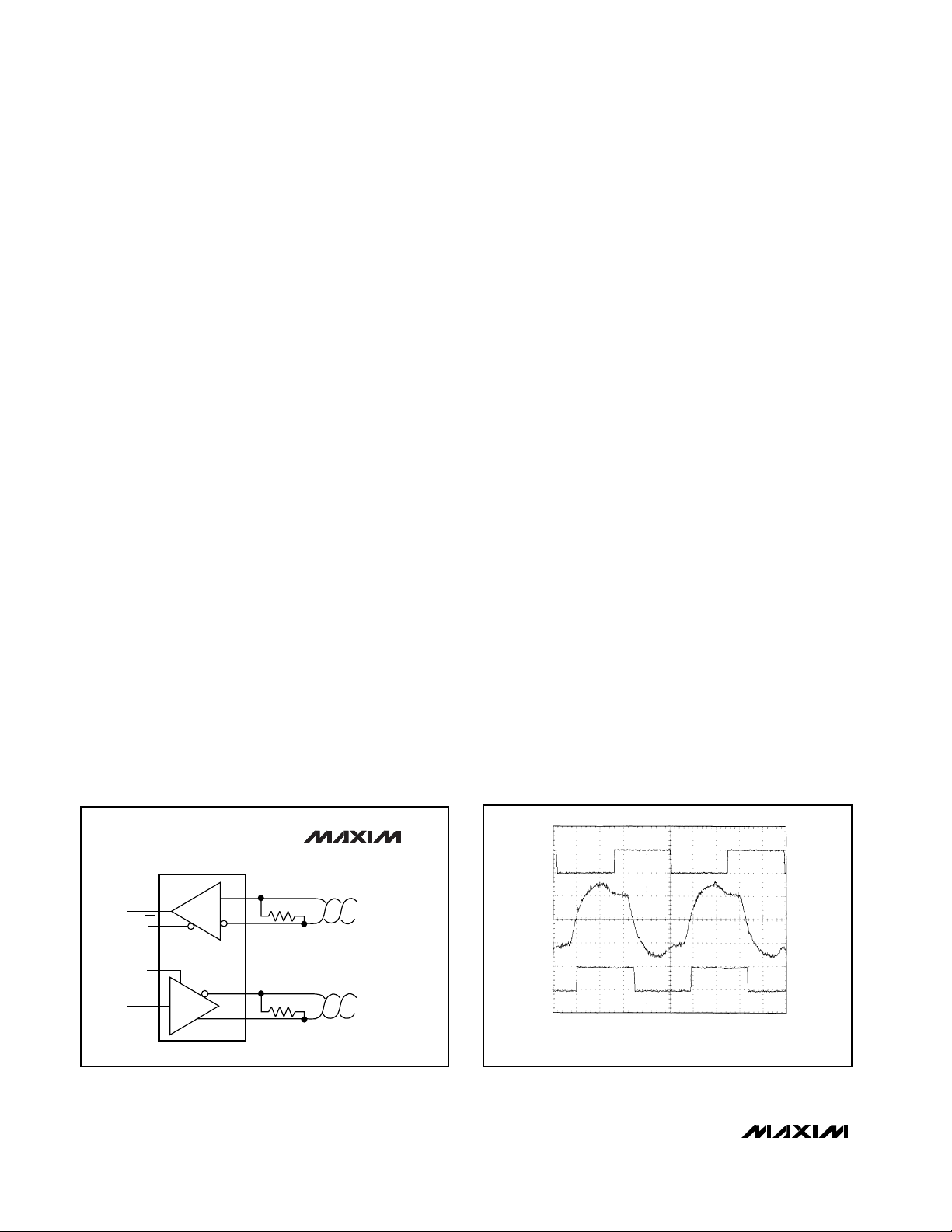
SIGNAL 2
SIGNAL 1
V
A
- V
B
BAUD PERIOD
t
ISI
Figure 12. Inter-Symbol Interference among Two Data
Patterns: Signal 1 = 11111110, Signal 2 = 00000010
100ns
0010101
1
10
V
Y
- V
Z
DI
2.5V/div
5V/div
Figure 13. Typical Preemphasis Waveform with a 100ns
Preemphasis Interval

Setting the Preemphasis Interval
The MAX3291 has an internal fixed preemphasis interval
of 100ns. Use the MAX3291 for existing designs requiring
industry-standard ’75180 pin-compatibility at data rates of
5Mbps to 10Mbps.
The MAX3292 has a resistor-programmable preemphasis
interval for more flexibility. For data rates less than 1Mbps,
use the following equation to calculate R
PSET
(the pre-
emphasis setting resistor):
R
PSET
= 580 (t
BAUD
- 100)
where t
BAUD
= one baud period in ns.
For example, a baud rate of 500kbps produces a baud
period of 2µs (2µs = 2000ns).
R
PSET
= 580 (t
BAUD
- 100)
R
PSET
= 580 (2000 - 100) = 1.1MΩ
For data rates of 1Mbps to 10Mbps, use the following
equation to calculate R
PSET
:
R
PSET
= 580 (t
BAUD
- 100)(t
BAUD
/ 1000)
where t
BAUD
= one baud period in ns.
For example, a baud rate of 1Mbps produces a baud
period of 1µs (1µs = 1000ns).
R
PSET
= 580 (1000 - 100)(1000 / 1000) = 522kΩ
(closest standard value is 523kΩ)
Set the preemphasis interval by connecting the R
PSET
resistor from PSET to VCC. Use a 0.1µF bypass capacitor (C
PSET
) from PSET to VCC. If PSET is connected
directly to VCC(R
PSET
= 0), the preemphasis interval
reverts to the nominal 100ns value.
Eye Diagrams
One simple method to quickly determine your circuit
configuration is to view an eye diagram. An eye diagram is a scope photo (voltage vs. time) showing the
transitions of a pseudo-random bit string displaying at
least one bit interval. Use an eye diagram to quickly
calculate the total jitter of a circuit configuration. Jitter is
the total time variation at the zero-volt differential crossing, and percent jitter is expressed as a percentage of
one baud period, t
BAUD
. Figures 15 and 16 show typical eye diagrams for a non-preemphasis device and
the MAX3291/MAX3292. ISI and jitter are often used
interchangeably; however, they are not exactly the
same thing. ISI usually makes up the majority of the jitter, but asymmetrical high and low driver output voltage
levels and time skews of non-ideal transceivers (driver
and receiver) also contribute to jitter.
MAX3291/MAX3292
RS-485/RS-422 Transceivers with Preemphasis
for High-Speed, Long-Distance Communication
______________________________________________________________________________________ 11
10,000
100
0.1 1 10
DATA RATE (Mbps)
CABLE LENGTH (FEET)
1000
10% JITTER
PREEMPHASIS
485 DRIVER
LIMIT
CONVENTIONAL
485 DRIVER
LIMIT
PREEMPHASIS REQUIRED
FOR ERROR-FREE
TRANSMISSION
24-GAUGE
TWISTED PAIR
Figure 14. Preemphasis Driver Performance Compared to a
Conventional Driver Without Preemphasis at 10% Jitter
Figure 15. Eye Diagram of a Typical RS-485 Transceiver
Without Preemphasis, while Driving 1000 feet of Cable at
5Mbps
Figure 16. Eye Diagram of the MAX3292 with a Preemphasis
Interval of 175ns, while Driving 1000 feet of Cable at 5Mbps
MAX3291/MAX3292
% Jitter = (total jitter / t
BAUD
) · 100
When the total amount of time skew becomes 10% or
more of the baud period, the data error rate can
increase sharply.
128 Transceivers on the Bus
The standard RS-485 receiver input impedance is 12kΩ
(one unit load), and the standard driver can drive up to
32 unit loads. The MAX3291/MAX3292 transceivers have
a 1/4-unit-load receiver input impedance (48kΩ), allowing up to 128 transceivers to be connected in parallel on
one communication line. Any combination of these
devices and/or other RS-485 transceivers with a total of
32 unit-loads or less can be connected to the line.
Low-Power Shutdown Mode
Initiate low-power shutdown mode by bringing RE high
and DE low. In shutdown the MAX3291/MAX3292 typically draw only 1µA of supply current.
Simultaneously driving RE and DE is allowed; the parts
are guaranteed not to enter shutdown if RE is high and
DE is low for less than 80ns. If the inputs are in this
state for at least 300ns, the parts are guaranteed to
enter shutdown.
Enable times tZHand tZLin the
Switching Characteris-
tics
tables correspond to when the part is not in the low-
power shutdown state. Enable times t
ZH(SHDN)
and
t
ZL(SHDN)
assume the parts are shut down. It takes drivers and receivers longer to activate from the lowpower shutdown mode (t
ZH(SHDN)
, t
ZL(SHDN)
) than from
the driver/receiver disable mode (tZH, tZL).
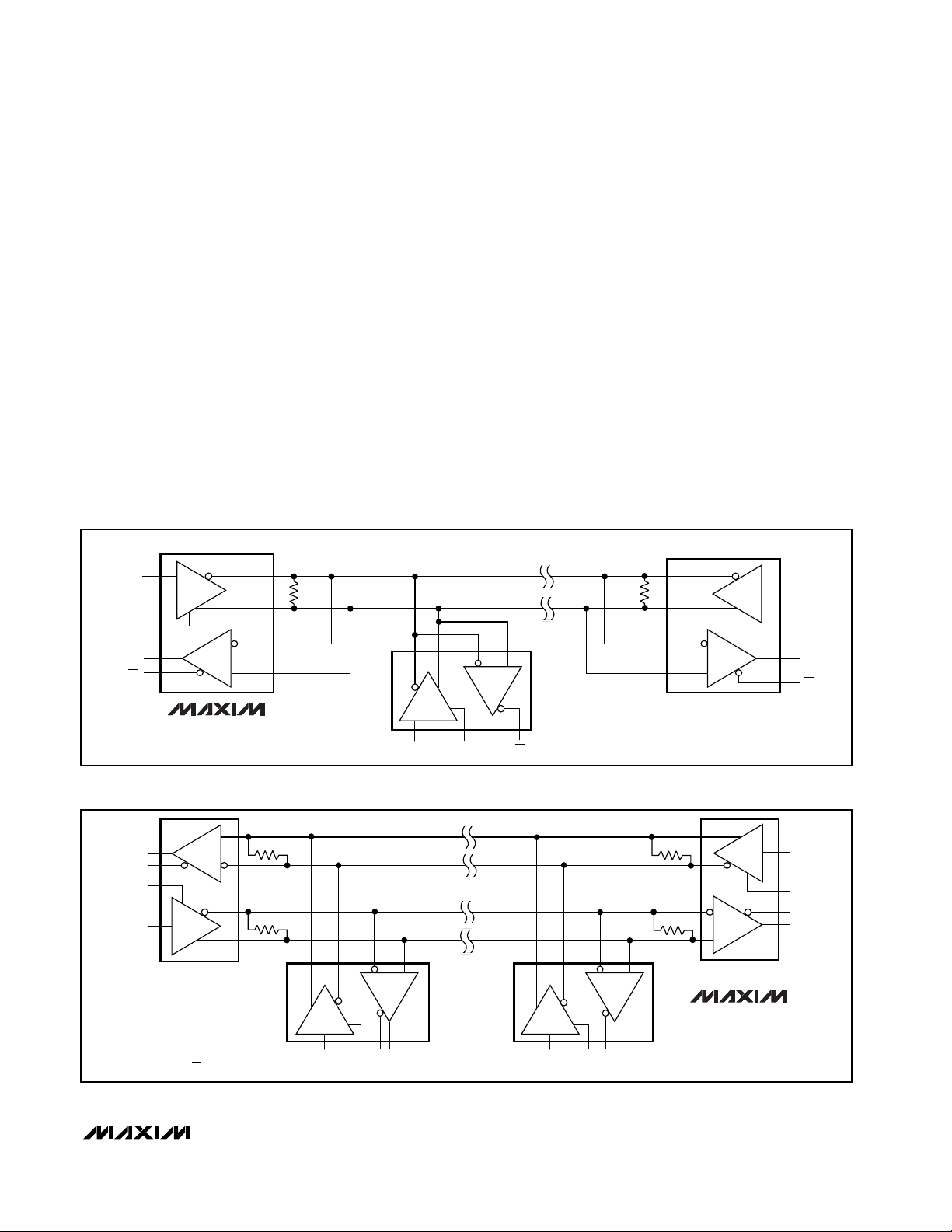
Line Repeater
For line lengths greater than what one MAX3291/
MAX3292 can drive, use the repeater application
shown in Figure 17.
Figure 18 shows the system differential voltage for the
MAX3292 driving 4000 feet of 26AWG twisted-pair wire
into two 120Ω termination loads.
Line Termination
The MAX3291/MAX3292 are targeted for applications
requiring the best combination of long cable length and
lowest bit-error rate. In order to achieve this combination, the cable system must be set up with care. There
are three basic steps:
1) The cable should only have two ends (no tree configuration with long branches), which are terminated with
a simple resistor termination whose value is the
cable’s characteristic impedance (ZO). Avoid terminations anywhere else along the cable. This ensures that
there are no reflections at the end of the cable, and
that all transmitters (whether they are located at the
ends of the cable or somewhere along the length) see
the same impedance, equal to ZO/ 2.
2) Make all branches or stubs short enough so that
twice the propagation delay along the stub (down
and back) is significantly less than one baud period
(around 15% or less). This ensures that the reflections from the end of the stub (which are unavoidable, since the stubs are not terminated) settle in
much less than a baud period. If the application
requires a branch much longer than this, use a
repeater (see the
Line Repeater
section).
RS-485/RS-422 Transceivers with Preemphasis
for High-Speed, Long-Distance Communication
12 ______________________________________________________________________________________
Figure 17. Line-Repeater Application
2µs/div
V
A
- V
B
RO
DI
RECEIVER
INPUT
1V/div
5V/div
TYPICAL OPERATING CIRCUIT, R
PSET
= 1MΩ
5V/div
Figure 18. MAX3292 System Differential Voltage Driving 4000
Feet, Using Two 120
Ω
Termination Resistors
MAX3291
MAX3292
A
RO
RE
DE
DI
D
R
120Ω
B
Z
120Ω
Y
DATA IN
DATA OUT
MAX3291/MAX3292
RS-485/RS-422 Transceivers with Preemphasis
for High-Speed, Long-Distance Communication
______________________________________________________________________________________ 13
DI RO
RE
Z
Z
Z
Y
B
A
YBA
RE
RE
RO
RO
DI
DI
DE
DE
DE
D
D
R
R
Y
B
A
R = Z
O
R = Z
O
D
R
MAX3291
MAX3292
Figure 19. Typical Half-Duplex RS-485 Network
3) Don’t overload the cable with too many receivers.
Even though the MAX3291/MAX3292 receives present only 1/4-unit load, placing 128 receivers on the
cable will attenuate the signal if spaced out along
the cable and, in addition, cause reflections if
clumped in one spot. The MAX3291/MAX3292 successfully drive the cables to correct RS-485/RS-422
levels with 128 receivers, but the preemphasis
effect is significantly diminished.
The MAX3291/ MAX3292 are centered for a load impedance of 54Ω, which corresponds to the parallel combination of the cable impedance and termination resistors. If
your cable impedance deviates somewhat from this
value, you still get the preemphasis effect (although the
ideal preemphasis time, t
PRE
, may need adjustment).
However, if your cable impedance is significantly different, the preemphasis ratio DPER changes, resulting in
significantly less preemphasis. Determine the preemphasis ratio versus load by referring to the Driver Differential
Output Voltage vs. R
DIFF
graph in the
Typical Operating
Characteristics
. Read the strong and normal levels from
the graph (remember that the horizontal units are half
your cable impedance) and divide the two numbers to
get DPER (DPER = V
STRONG
/ V
NORMAL
= V
ODP
/ VOD).
Figures 19 and 20 show typical network application circuits with proper termination.
Preemphasis at Low Data Rates
(MAX3292)
At low data rates (<1Msps), preemphasis operation is
not guaranteed because it is highly dependent on the
system power-supply noise. Minimize this noise by
increasing bypass capacitance and using a power
supply with a fast transient response.
R = Z
O
R = Z
O
R
D
RO
RE
DE
DI
A
B
Y
R = Z
O
R = Z
O
DI
DI DIRO RO
RO
DE DE
DE
RE
RE
RE
Z
Z
Z
Z
Y
Y
Y
AA
A
BB
B
D
D
D
R
R
R
MAX3291
MAX3292
NOTE: RE AND DE ON.
Figure 20. Typical Full-Duplex RS-485 Network

MAX3291/MAX3292
RS-485/RS-422 Transceivers with Preemphasis
for High-Speed, Long-Distance Communication
14 ______________________________________________________________________________________
Chip Information
TRANSISTOR COUNT: 2280
SUBSTRATE CONNECTED TO GND
Pin Configuration
14
13
12
11
10
9
8
1
2
3
4
5
6
7
V
CC
N.C. (PVCC)
A
BDE
RE
RO
PEE (PSET)
TOP VIEW
MAX3291
MAX3292
Z
Y
N.C.
( ) ARE FOR THE MAX3292 ONLY.
GND
N.C. (GND)
DI
SO/DIP
MAX3291/MAX3292
RS-485/RS-422 Transceivers with Preemphasis
for High-Speed, Long-Distance Communication
______________________________________________________________________________________ 15
________________________________________________________Package Information
SOICN.EPS

MAX3291/MAX3292
RS-485/RS-422 Transceivers with Preemphasis
for High-Speed, Long-Distance Communication
Maxim cannot assume responsibility for use of any circuitry other than circuitry entirely embodied in a Maxim product. No circuit patent licenses are
implied. Maxim reserves the right to change the circuitry and specifications without notice at any time.
16
____________________Maxim Integrated Products, 120 San Gabriel Drive, Sunnyvale, CA 94086 408-737-7600
© 1999 Maxim Integrated Products Printed USA is a registered trademark of Maxim Integrated Products.
___________________________________________Package Information (continued)
PDIPN.EPS
 Loading...