For free samples & the latest literature: http://www.maxim-ic.com, or phone 1-800-998-8800.
For small orders, phone 1-800-835-8769.
General Description
The MAX3286/MAX3296 series of products are highspeed laser drivers for fiber optic LAN transmitters,
optimized for Gigabit Ethernet applications. Each
device contains a bias generator, laser modulator, and
comprehensive safety features. Automatic power control (APC) adjusts the laser bias current to maintain
average optical power at a constant level, regardless of
changes in temperature or laser properties. For lasers
without a monitor photodiode, these products offer a
constant-current mode. The circuit can be configured
for use with conventional shortwave (780nm to 850nm)
or longwave (1300nm) laser diodes, as well as verticalcavity surface-emitting lasers (VCSELs).
The MAX3286 series (MAX3286/MAX3287/MAX3288/
MAX3289) is optimized for operation at 1.25Gbps, and
the MAX3296 series (MAX3296/MAX3297/MAX3298/
MAX3299) is optimized for 2.5Gbps operation. Each
device can switch 30mA of laser modulation current at
the specified data rate. Adjustable temperature compensation is provided to keep the optical extinction
ratio within specifications over the operating temperature range. This series of devices is optimized to drive
lasers packaged in low-cost TO-46 headers. Deterministic jitter (DJ) for the MAX3286 is typically 22ps,
allowing a 72% margin to Gigabit Ethernet DJ specifications.
These laser drivers provide extensive safety features to
guarantee single-point fault tolerance. Safety features
include dual enable inputs, dual shutdown circuits, and
a laser-power monitor. The safety circuit detects faults
that could cause dangerous light output levels. A programmable power-on reset pulse initializes the laser
driver at start-up.
The MAX3286/MAX3296 are available in a compact,
5mm x 5mm, 32-pin TQFP package or in die form. The
MAX3287/MAX3288/MAX3289 and MAX3297/MAX3298/
MAX3299 are available in smaller 16-pin TSSOP-EP
packages, which are ideal for small form-factor optical
modules.
Applications
Gigabit Ethernet Optical Transmitter
Fibre Channel Optical Transmitter
ATM LAN Optical Transmitter
Features
♦ 7ps Deterministic Jitter (MAX3296)
22ps Deterministic Jitter (MAX3286)
♦ +3.0V to +5.5V Supply Voltage
♦ Selectable Laser Pinning (common cathode or
common anode) (MAX3286/MAX3296)
♦ 30mA Laser Modulation Current
♦ Temperature Compensation of Modulation
Current
♦ Automatic Laser Power Control or Constant Bias
Current
♦ Integrated Safety Circuits
♦ Power-On Reset Signal
♦ 16-Pin TSSOP-EP Package Available
MAX3286–MAX3289/MAX3296–MAX3299
3.0V
to
5.5V, 1.25Gbps/2.5Gbps
LAN Laser Drivers
________________________________________________________________ Maxim Integrated Products 1
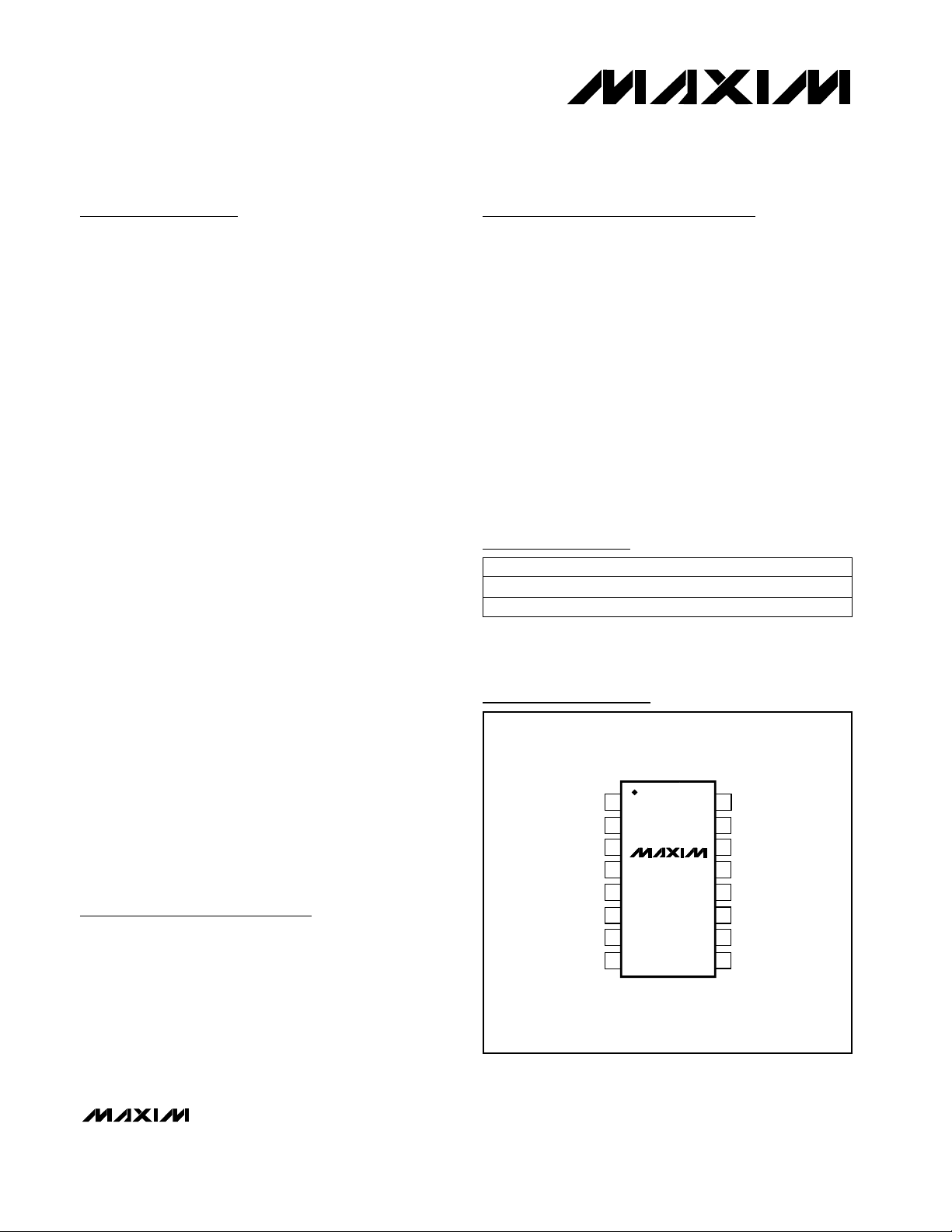
16
15
14
13
12
11
10
9
1
2
3
4
5
6
7
8
GND TC
MODSET
V
CC
OUT-
OUT+
V
CC
BIASDRV
SHDNDRV
TOP VIEW
MAX3287
MAX3289
MAX3297
MAX3299
TSSOP-EP*
FLTDLY
V
CC
GND
IN+
IN-
REF
MD
19-1550; Rev 0; 12/99
PART
MAX3286CHJ
MAX3286C/D 0°C to +70°C
0°C to +70°C
TEMP. RANGE PIN-PACKAGE
32 TQFP (5mm x 5mm)
Dice*
Ordering Information continued at end of data sheet.
*Dice are designed to operate from T
J
= 0°C to +110°C, but are
tested and guaranteed only at TA= +25°C.
Pin Configurations
Ordering Information
Typical Application Circuits and Selector Guide appear at
end of data sheet.
*Exposed paddle is connected to GND.
Pin Configurations continued at end of data sheet.

MAX3286–MAX3289/MAX3296–MAX3299
3.0V to 5.5V, 1.25Gbps/2.5Gbps
LAN Laser Drivers
2 _______________________________________________________________________________________
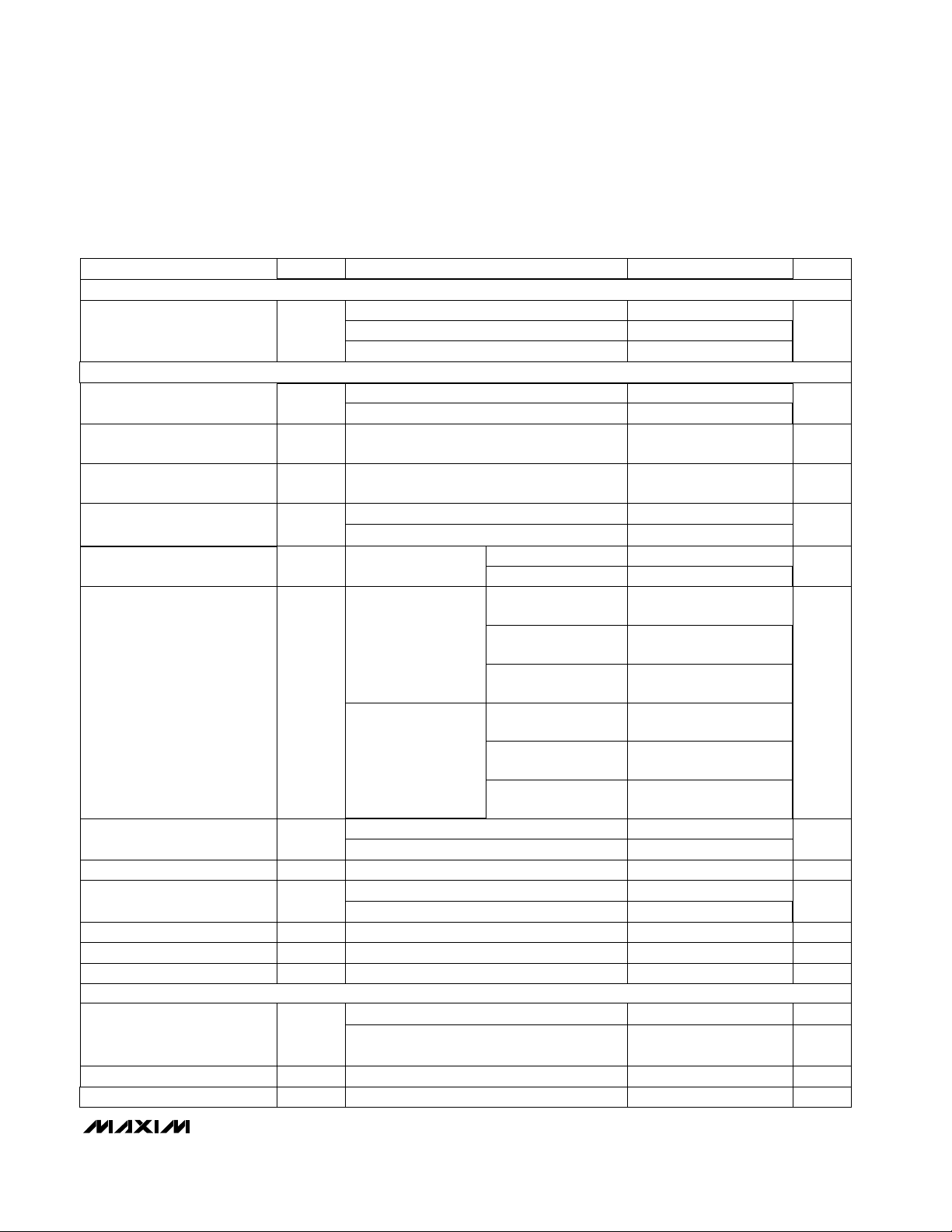
ABSOLUTE MAXIMUM RATINGS
ELECTRICAL CHARACTERISTICS
(VCC= +3.0V to +5.5V, TA= 0°C to +70°C, unless otherwise noted. Typical values are at VCC= +3.3V and TA= +25°C, RTC= open;
see Figure 1a.)
Stresses beyond those listed under “Absolute Maximum Ratings” may cause permanent damage to the device. These are stress ratings only, and functional
operation of the device at these or any other conditions beyond those indicated in the operational sections of the specifications is not implied. Exposure to
absolute maximum rating conditions for extended periods may affect device reliability.
Supply Voltage at VCC..........................................-0.5V to +7.0V
Voltage at
EN, EN, PORDLY, FLTDLY, LV, IN+, IN-,
REF, POL, POL, MD, MON, BIASDRV,
MODSET, TC..........................................................-0.5V to (V
CC
+ 0.5V)
Voltage at OUT+, OUT-.........................(V
CC
- 2V) to (VCC+ 2V)
Current into FAULT, FAULT, POR, SHDNDRV....-1mA to +25mA
Current into OUT+, OUT- ....................................................60mA
Continuous Power Dissipation (T
A
= +70°C)
32-Pin TQFP (derate 14.3mW/°C) ...............................1100mW
16-Pin TSSOP (derate 27mW/°C)................................2162mW
Operating Temperature Range...............................0°C to +70°C
Operating Junction Temperature Range ..............0°C to +150°C
Processing Temperature (die) .........................................+400°C
Storage Temperature Range .............................-55°C to +150°C
Lead Temperature (soldering, 10s) .................................+300°C
0 ≤ V
PIN
≤ V
CC
Total differential signal, peak-peak, Figure 1a
LV = open
Figure 1a, R
MOD
= 1.82kΩ
LV = GND
V
MON
= V
CC
I
REF
≤ 2mA, MON = V
CC
FAULT = low, V
BIASDRV
≥ 0.6V
Normal operation (FAULT = low)
EN = GND
IOH= -100µA
Common-cathode configuration
IOL= 1mA
APC loop is closed
CONDITIONS
V
MD
+ 5% V
MD
+ 20%MD High Fault Threshold
V2.95REF Fault Threshold
mV150POR Hysteresis
2.65 3.0
V
3.9 4.5
POR Threshold
µA0.44 6MON Input Current
µA-2 0.16 2MD Input Current
V
0.4 1.2
V1.55 1.7 1.85V
MD
MD Nominal Voltage
µA-100 100TTL Input Current
mV200 1660V
ID
mA52 75I
CC
Supply Current
Data Input Voltage Swing
V2.45 2.65 2.85REF Voltage
mA
0.8BIASDRV Current Sink
µA-1 1BIASDRV Current, Shutdown
V2.0V
IH
TTL Input High Voltage
V0.8V
IL
TTL Input Low Voltage
V2.4V
OH
FAULT, FAULT Output High
Voltage
V0.4V
OL
FAULT, FAULT Output Low
Voltage
UNITSMIN TYP MAXSYMBOLPARAMETER
Common-anode configuration 2VCC- 0.8
MD Voltage During Fault
V
MD
- 20% V
MD
- 5%MD Low Fault Threshold
MAX3286/MAX3288/MAX3296/MAX3298
mV
VCC- V
CC -
600 480
MON Fault Threshold
V
0.8MODSET, TC Fault Threshold
FAULT = low, V
BIASDRV
≤ VCC- 1V 0.8BIASDRV Current Source
BIAS GENERATOR (Note 1)
POWER-ON RESET
FAULT DETECTION
MAX3286–MAX3289/MAX3296–MAX3299
3.0V to 5.5V, 1.25Gbps/2.5Gbps
LAN Laser Drivers
________________________________________________________________________________________ 3
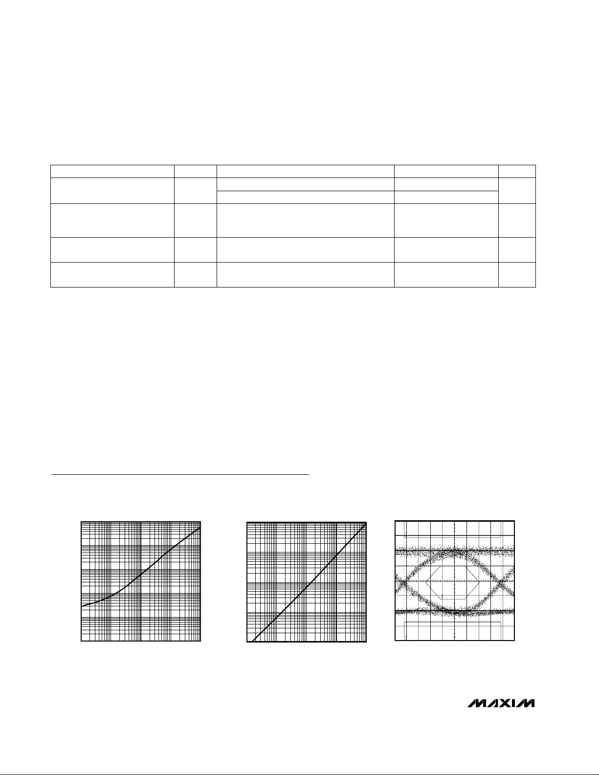
ELECTRICAL CHARACTERISTICS (continued)
(VCC= +3.0V to +5.5V, TA= 0°C to +70°C, unless otherwise noted. Typical values are at VCC= +3.3V and TA= +25°C, RTC= open;
see Figure 1a.)
I
SHDNDRV
= 15mA, FAULT not asserted
I
SHDNDRV
= 10µA, FAULT asserted
MAX3296 series
MAX3286 series
I
SHDNDRV
= 1mA, FAULT not asserted
MAX3286 series
MAX3296 series
Tempco = max, R
MOD
= open; Figure 5
CONDITIONS
Ω620 800 980Differential Input Resistance
ppm/°C
4000
Modulation-Current
Temperature Coefficient
0V
CC
- 1.2
V
VCC- 0.4
Voltage at SHDNDRV
µA15 200Shutdown Modulation Current
24
ps
28
Random Jitter, RMS (Note 3)
0V
CC
- 2.4
Gbps
1.25
Data Rate
2.5
UNITS
MIN TYP MAXSYMBOL
PARAMETER
mA
2
Minimum Laser Modulation
Current
MAX3286 series
20% to 80% ps
130 220
Modulation-Current Edge
Speed
MAX3296 series 90 150
R
MOD
= 13kΩ
(i
MOD
= 5mA)
MAX3286 series
ps
46 65
Deterministic Jitter (Note 2)
R
MOD
= 4.1kΩ
(i
MOD
= 15mA)
29 45
R
MOD
= 1.9kΩ
(i
MOD
= 30mA)
22 35
R
MOD
= 13kΩ
(i
MOD
= 5mA)
MAX3296 series
14 35
R
MOD
= 4.1kΩ
(i
MOD
= 15mA)
822
R
MOD
= 1.9kΩ
(i
MOD
= 30mA)
720
C
PORDLY
= 0.01µF,
MAX3286/MAX3296 only
ms3 5.5
(Note 4)
µsGlitch Rejection at MD 10 20
µs22t
FAULT
Fault Time
SHUTDOWN
LASER MODULATOR
50Tempco = min, RTC= open; Figure 5
R
MOD
= 13kΩ (i
MOD
= 5mA) -15 15
Single ended Ω42 50 58Output Resistance
LASER SAFETY CIRCUIT
PORDLY = open 0.3 1.25 µs
t
PORDLY
POR Delay
V
V
CC
- 0.3
Input Bias Voltage
RL≤ 25Ω mA30
Maximum Laser Modulation
Current
R
MOD
= 1.9kΩ (i
MOD
= 30mA)
%
-10 10
Tolerance of Modulation Current
MAX3286–MAX3289/MAX3296–MAX3299
3.0V to 5.5V, 1.25Gbps/2.5Gbps
LAN Laser Drivers
4 _______________________________________________________________________________________
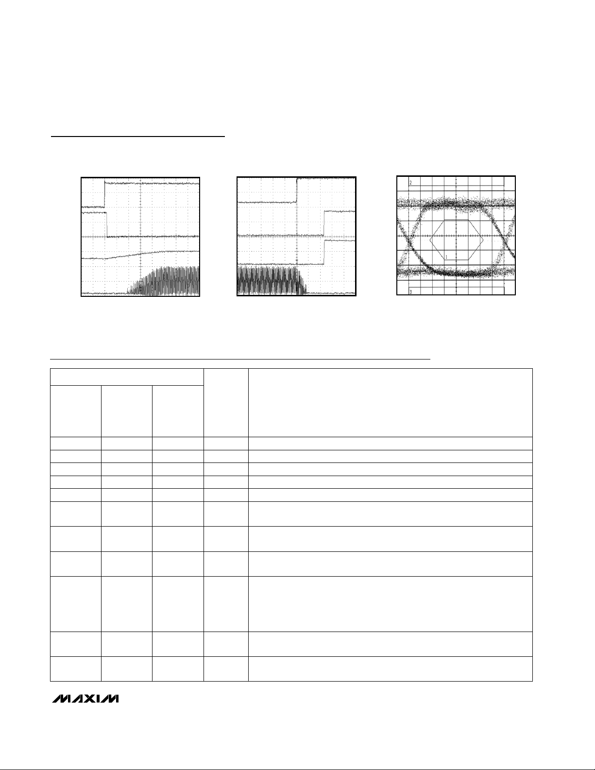
Typical Operating Characteristics
(TA = +25°C, unless otherwise noted.)
POR DELAY vs. C
PORDLY
MA3286 toc01
CAPACITANCE (pF)
DELAY (µs)
10k
100k
1
10
100
1k
100 1k 10k10 100k
FLTDLY DURATION vs. C
FLTDLY
MA3286 toc02
CAPACITANCE (pF)
DELAY (µs)
10k
1
10
100
1k
100 1k 10k101
Note 1: “Common-anode configuration” refers to a configuration where POL = GND, POL = VCC, and an NPN device is used to set
the laser bias current. “Common-cathode configuration” refers to a configuration where POL = V
CC
, POL = GND, and a PNP
device is used to set the laser bias current.
Note 2: Deterministic jitter measured with a repeating K28.5 bit pattern 00111110101100000101. Deterministic jitter is the peak-to-
peak deviation from the ideal time crossings per ANSI X3.230, Annex A.
Note 3: For Fibre Channel and Gigabit Ethernet applications, the peak-to-peak random jitter is 14.1 times the RMS jitter.
Note 4: Delay from a fault on MD until FAULT is asserted high.
ELECTRICAL CHARACTERISTICS (continued)
(VCC= +3.0V to +5.5V, TA= 0°C to +70°C, unless otherwise noted. Typical values are at VCC= +3.3V and TA= +25°C, RTC= open;
see Figure 1a.)
MAX3286/MAX3296 only,
Figure 1b
C
FLTDLY
= 270pF
C
FLTDLY
= 0
MAX3286/MAX3296 only,
Figure 1b
MAX3286/MAX3296 only,
Figure 1b
CONDITIONS
ns610t
EN_RESET
EN or EN Minimum Pulse Width
Required to Reset a Latched
Fault
100 140
µs
0.2 1
t
FLTDLY
FLTDLY Duration
µs3.5 5.5t
SHUTDN
SHDNDRV Asserted After EN =
low or EN = high
µs12t
RESET
FAULT Reset After EN, EN, or
POR Transition
UNITSMIN TYP MAXSYMBOLPARAMETER
2.5Gbps, 1310nm Laser, 27 - 1 PRBS, i
EYE DIAGRAM
50ps/div
MOD
MAX3286 toc03
= 15mA
MAX3286–MAX3289/MAX3296–MAX3299
3.0V to 5.5V, 1.25Gbps/2.5Gbps
LAN Laser Drivers
_______________________________________________________________________________________ 5
Pin Description
NAME FUNCTION
MAX3286
MAX3296
1
FAULT
Inverting Fault Indicator. See Table 1.
PIN
2, 16 N.C. No Connect
3 FAULT Noninverting Fault Indicator. See Table 1.
4 POR Power-On Reset. POR is a TTL-compatible output. See Figure 14.
5, 14, 22, 30 GND Ground
6 EN
Enable TTL Input. Laser output is enabled only when EN is high and EN is
low. If EN is left unconnected, the laser is disabled.
7
EN
Inverting Enable TTL Input. Laser output is enabled only when EN is low or
grounded and EN is high. If EN is left unconnected, the laser is disabled.
8 PORDLY
Power-On Reset Delay. To extend the delay for the power-on reset circuit,
connect a capacitor to PORDLY. See Design Procedure.
9 FLTDLY
Fault Delay Input. Determines the delay of the FAULT and FAULT outputs.
A capacitor attached to FLTDLY ensures proper start-up. (See Typical
Operating Characteristics.) FLTDLY = GND: holds FAULT low and FAULT
high. When FLTDLY = GND, EN = high, EN = low, and V
CC
is within the
operational range, the safety circuitry is inactive.
10 LV
Low-Voltage Operation. Connect to GND for 4.5V to 5.5V operation. Leave
open for 3.0V to 5.5V operation.
MAX3287
MAX3297
MAX3289
MAX3299
—
—
—
—
1, 6
—
—
—
2
—
MAX3288
MAX3298
—
—
—
—
1, 6
—
—
—
2
—
Typical Operating Characteristics (continued)
(TA = +25°C, unless otherwise noted.)
EN STARTUP
(COMMON-ANODE CONFIGURATION)
MA3286 toc04
EN
OPTICAL
OUTPUT
BIASDRV
FAULT
5µs/div
MD SHUTDOWN
MA3286 toc05
MD
OPTICAL
OUTPUT
SHDNDRV
FAULT
10µs/div
EYE DIAGRAM
MA3286 toc06
50ps/div
2.5Gbps, 1310nm LASER, 2
7
- 1 PRBS, i
mod
= 15mA
11, 25,
26, 29
V
CC
Supply Voltage3, 11, 14 3, 11, 14

MAX3286–MAX3289/MAX3296–MAX3299
3.0V to 5.5V, 1.25Gbps/2.5Gbps
LAN Laser Drivers
6 _______________________________________________________________________________________
Pin Description (continued)
MD
FAULT CONDITION
V
CC
VMD> 1.15 · V
MD(nom)
,
V
MD
< 0.85 · V
MD(nom)
LV = open and VCC< 3V;
LV = GND and VCC< 4.5V
REF
EN and EN
V
REF
> 2.95V
PIN
POL and POL
EN = low or open, EN = high or open
POL = POL
MON V
MON
< VCC- 540mV
Table 1. Typical Fault Conditions
>4.5Grounded
>3.0Open
OPERATING VOLTAGE
RANGE (V)
LV
Table 2. LV Operating Range
MAX3288
MAX3298
MAX3287
MAX3297
MAX3289
MAX3299
PIN
MAX3286
MAX3296
FUNCTIONNAME
EPEP
Ground. This must be soldered to the circuit board ground for proper
thermal performance. See Layout Considerations.
Exposed
Paddle
—
16
15
5
4
16
15
5
4
Temperature-Compensation Set. The resistor at TC programs the temperature-increasing component of the laser modulation current.
TC32
Modulation-Current Set. The resistor at MODSET programs the temperature-stable component of the laser modulation current.
MODSET31
Inverting Data InputIN-13
Noninverting Data InputIN+12
MODSET
and TC
V
MODSET
and VTC≤ 0.8V
13
12
13
12
Modulation-Current Output. See Typical Application Circuits.OUT-28
Modulation-Current Output. See Typical Application Circuits.OUT+27
—
7
—
7
Polarity Input. POL is used for programming the laser-pinning polarity.
(Table 4)
POL17
Reference Voltage. A resistor connected at REF to MD determines the
laser power when APC is used with common-cathode lasers.
REF15
9
8
—
8
Laser Bias Current Monitor. Used for programming laser bias current in
VCSEL applications.
MON21
Monitor Diode Connection. MD is used for automatic power control.MD20
—
—
—
—
Internally Connected. Do not connect.I.C.19
Inverting Polarity Input. POL is used for programming the laser-pinning
polarity (Table 4)
POL
18
10
—
10
9
Bias-Controlling Transistor Driver. Connects to the base of an external
PNP or NPN transistor.
BIASDRV24
Shutdown Driver Output. Provides a redundant laser shutdown.SHDN-DRV23
MAX3286–MAX3289/MAX3296–MAX3299
3.0V to 5.5V, 1.25Gbps/2.5Gbps
LAN Laser Drivers
_______________________________________________________________________________________ 7
MODULATION
CONTROL
MODSET
TC
L = 3.9nH
L = 3.9nH
R
L
.= 25Ω
BIASDRV
LASER
EQUIVALENT
LOAD
(OPEN)
OUT- OUT+
FERRITE BEAD*
*MURATA
BLM11HA102
0.01µF
0.01µF
IN+
IN-
50Ω 50Ω
25Ω
R
L
R
MOD
V
CC
V
CC
V
CC
I
OUT
I
CC
V
CC
i
MOD
3/2
i
MOD
V
ID
VID = V
IN+ - VIN-
CURRENT
i
MOD
V
IN-
V
IN+
VOLTS
TIME
100mVp-p MIN
830mVp-p MAX
200mVp-p MIN
1660mVp-p MAX
DIFFERENTIAL INPUT
RESULTING SIGNAL
MAX3286
MAX3296
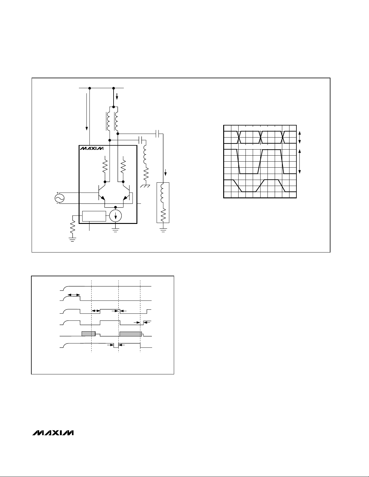
Figure 1a. Output Load for AC Specification
V
CC
POR
FAULT
FAULT ON MD RESET BY EN SHUTDOWN
BY EN
SHDNDRV
OPTICAL
OUT
EN
NOTE: TIMING IS
NOT TO SCALE.
t
PORDLY
t
FAULT
t
RESET
t
SHUTDN
t
EN_RESET
Figure 1b. Fault Timing
_______________Detailed Description
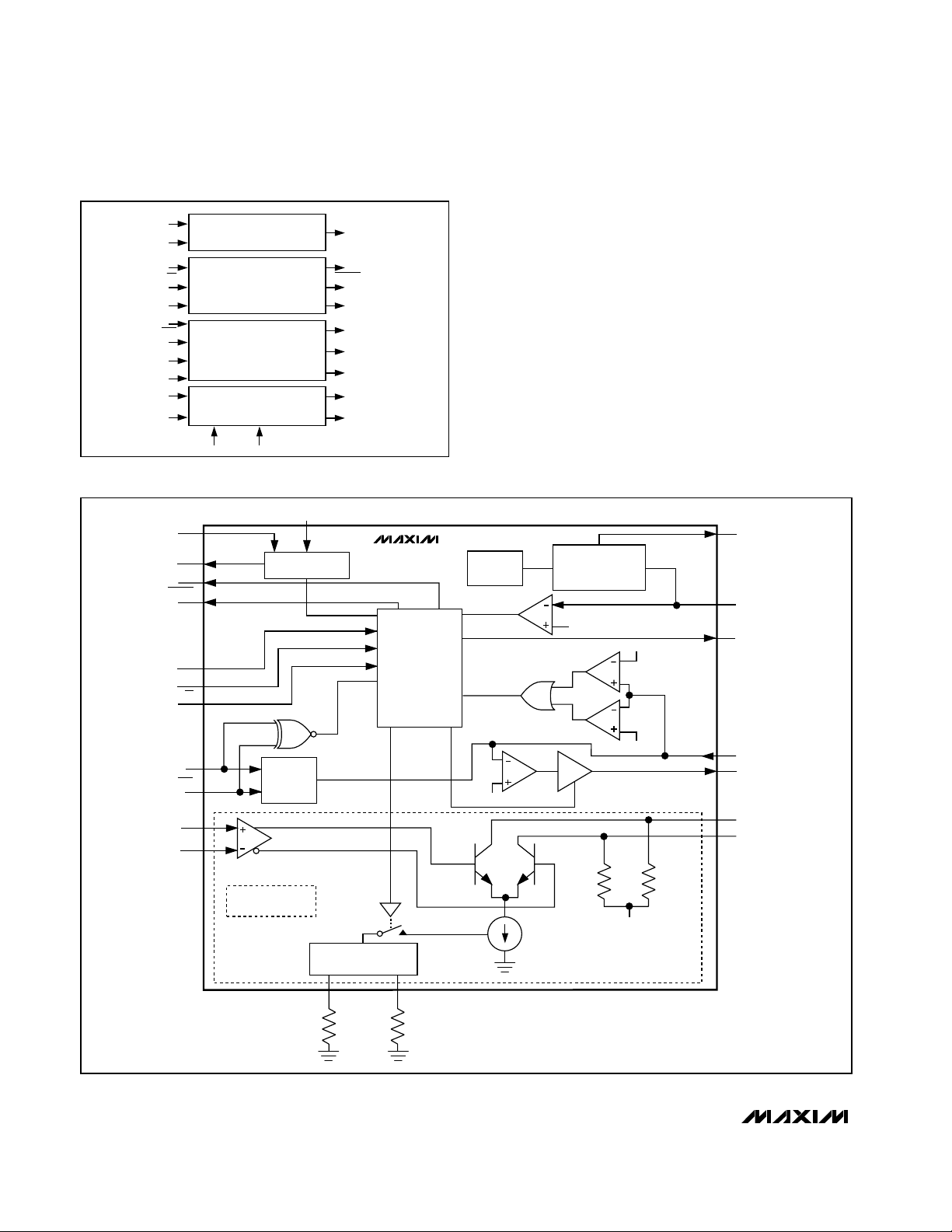
The MAX3286/MAX3296 series of laser drivers contain
a bias generator with automatic power control (APC),
laser modulator, power-on reset (POR) circuit, and
safety circuitry (Figures 2a and 2b).
Bias Generator
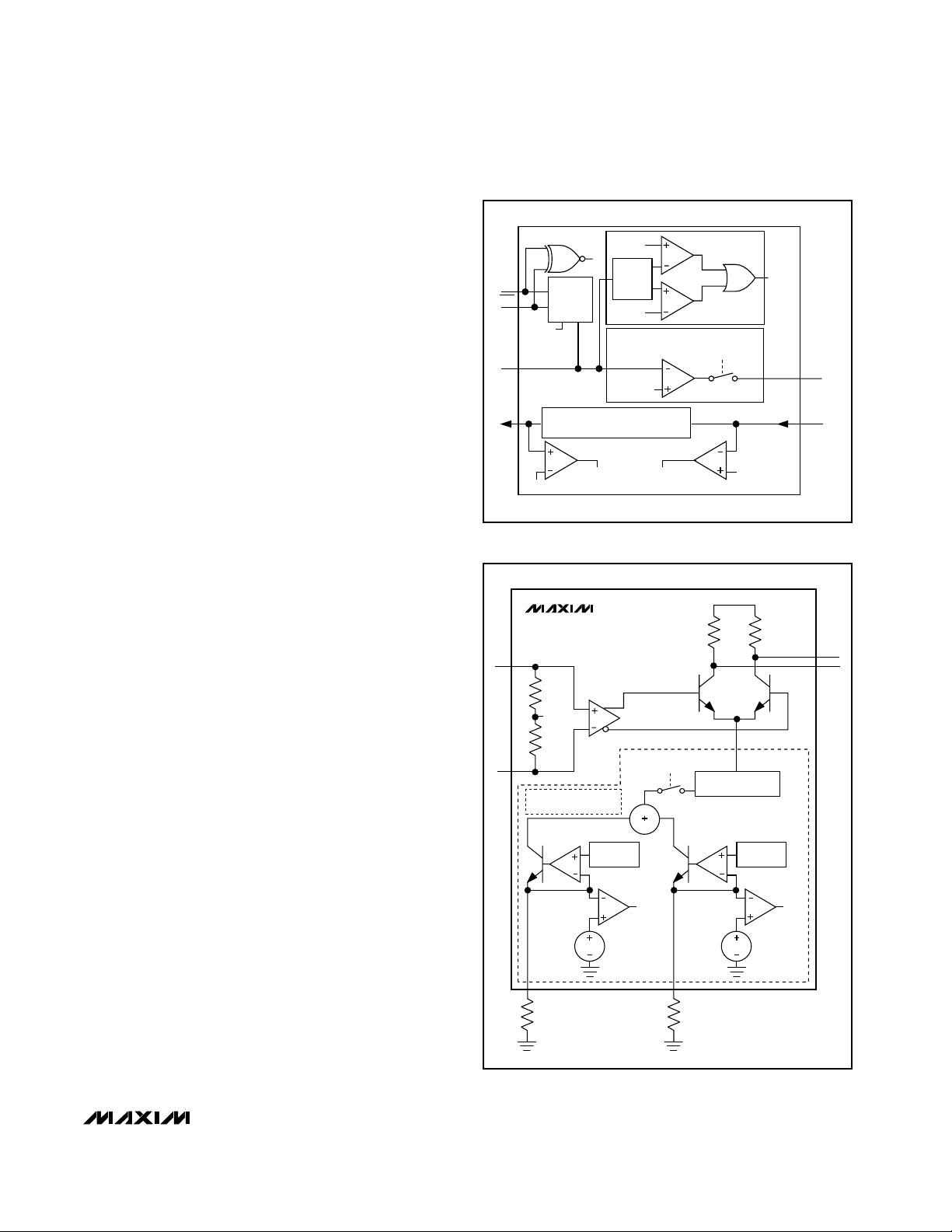
Figure 3 shows the bias generator circuitry containing a
power-control amplifier, controlled reference voltage,
smooth-start circuit, and window comparator. The bias
generator combined with an external PNP or NPN transistor provides DC laser current to bias the laser in a
light-emitting state. When there is a monitor diode (MD)
in the laser package, the APC circuitry adjusts the
laser-bias current to maintain average power over tem-
MAX3286–MAX3289/MAX3296–MAX3299
3.0V to 5.5V, 1.25Gbps/2.5Gbps
LAN Laser Drivers
8 _______________________________________________________________________________________
SMOOTH
START
IN+
IN-
TC MODSET
R
MOD
V
CC
R
TC
MON
SHDNDRV
REF
POR
PORDLY
POL
POL
FAULT
FAULT
FLTDLY
EN
EN
1.97V
LV
1.53V
+1.7V
50Ω 50Ω
CONTROLLED
REFERENCE
GENERATOR
LASER
MODULATOR
MODULATION CURRENT
GENERATOR
1.7V
REF
BIASDRV
MD
OUTOUT+
POR CIRCUIT
SAFETY
CIRCUITRY
INPUT BUFFER
VCC - 0.54V
MAX3286
MAX3296
BIAS GENERATOR
Figure 2b. Laser Driver Functional Diagram
LASER
MODULATOR
POR CIRCUIT
SAFETY
BIAS GENERATOR
MODSET
TC
BIASDRV
MD
SHDNDRV
FAULT
FAULT
POR
LV
PORDLY
EN
EN
FLTDLY
POL
POL
MON
MD
OUT-
OUT+
REF
IN+
IN-
Figure 2a. Simplified Laser Driver Functional Diagram
perature and changing laser properties. The MD input
is connected to the anode or cathode of a monitor photodiode or to a resistor-divider, depending on the specific
application circuit. Three application circuits are supported: common-cathode laser with photodiode, common-cathode laser without photodiode, and commonanode laser with photodiode (as shown in the Design
Procedure). The POL and POL inputs determine the laser
pinning (common cathode, common anode) (Table 4).
The smooth-start circuitry prevents current spikes to the
laser during power-up or enable; this ensures compliance
with safety requirements and extends the life of the laser.
The power-control amplifier drives an external transistor
to control the laser bias current. In a fault condition, the
power-control amplifier’s output is disabled (high
MAX3286–MAX3289/MAX3296–MAX3299
3.0V to 5.5V, 1.25Gbps/2.5Gbps
LAN Laser Drivers
_______________________________________________________________________________________ 9
impedance). This ensures that the PNP or NPN transistor
is turned off, removing the laser-bias current. (See
Applications Information.)
The REF pin provides a controlled reference voltage
dependent upon the voltage at MON. The voltage at
REF is V
REF
= 2.65 - 2.25(VCC- V
MON
). A resistor connected at REF determines the laser power when APC is
used with common-cathode lasers. See the Design
Procedure for setting the laser power.
Modulation Circuitry
The modulator circuitry consists of an input buffer, current
generator, and high-speed current switch (Figure 4). The
modulator drives up to 30mA of modulation current into
a 25Ω load.
Many of the modulator performance specifications
depend on the total modulator current (I
OUT
) (Figure 1a).
To ensure good driver performance, the voltage at
OUT+ and OUT- must not be less than VCC- 1V.
The amplitude of the modulation current is set with
resistors at the MODSET and TC (temperature coefficient)
pins. The resistor at MODSET (R
MOD
) programs the
temperature-stable portion of modulation current, while
the resistor at TC (RTC) programs the temperatureincreasing portion of the modulation current. Figure 5
shows modulation current as a function of temperature
for two extremes: RTCis open (the modulation current
has zero temperature coefficient) and R
MOD
is open
(the modulation temperature coefficient is 4000ppm).
Intermediate tempco values of modulation current can
be obtained as described in the Design Procedure.
Safety Circuitry
The laser driver can be used with two popular safety
systems. APC maintains laser safety using local feedback. Safety features monitor laser driver operation and
force a shutdown if a fault is detected. The shutdown
condition is latched until reset by a toggle of EN, EN, or
power.
Another safety system, Open Fiber Control (OFC), uses
safety interlocks to prevent eye hazards. To accommodate the OFC standard, the MAX3286/MAX3296 series
provide dual enable inputs and dual fault outputs.
The safety circuitry contains fault detection, dual enable
inputs, latched fault outputs, and a pulse generator
(Figure 6).
Safety circuitry monitors the APC circuit to detect unsafe
levels of laser emission during single-point failures. A
single-point failure can be a short to VCCor GND, or
between any two IC pins.
SMOOTH
START
POLARITY _FAULT
ENABLE
WINDOW
COMPARATOR
MD
FAULT
REF_FAULT MONITOR_FAULT
V
CC
- 540mV
BIASDRV
MON
POL
POL
MD
REF
POWER
CONTROL
AMPLIFIER
+1.7V
CONTROLLED REFERENCE VOLTAGE
V
REF
= 2.65 - 2.25 (VCC - V
MON
)
+1.97V
2.95V
+1.53V
GLITCH
REJECT
ENABLE
Figure 3. Bias Generator Circuitry
V
CC
CURRENT
SWITCH
INPUT
BUFFER
OUT+
OUT-
IN+
IN-
50Ω 50Ω
400Ω
400Ω
V
CC
- 0.3V
CURRENT AMPLIFIER
96X
4000ppm/°C
REFERENCE
ENABLE
0.8V
TC MODSET
R
TC
R
MOD
0.8V
TC_FAULT
MOD_FAULT
MODULATION CURRENT
GENERATOR
1.2V
REFERENCE
MAX3286
MAX3296
Figure 4. Laser Modulator Circuitry
 Loading...