

Page 1
现货库存、技术资料、百科信息、热点资讯,精彩尽在鼎好!
General Description
The MAX3286/MAX3296 series of products are highspeed laser drivers for fiber optic LAN transmitters optimized for Gigabit Ethernet applications. Each device
contains a bias generator, laser modulator, and comprehensive safety features. Automatic power control
(APC) adjusts the laser bias current to maintain average optical power at a constant level, regardless of
changes in temperature or laser properties. For lasers
without a monitor photodiode, these products offer a
constant-current mode. The circuit can be configured
for use with conventional shortwave (780nm to 850nm)
or longwave (1300nm) laser diodes, as well as verticalcavity surface-emitting lasers (VCSELs).
The MAX3286 series (MAX3286–MAX3289) is optimized for operation at 1.25Gbps, and the MAX3296
series (MAX3296–MAX3299) is optimized for 2.5Gbps
operation. Each device can switch 30mA of laser modulation current at the specified data rate. Adjustable
temperature compensation is provided to keep the optical extinction ratio within specifications over the operating temperature range. This series of devices is
optimized to drive lasers packaged in low-cost TO-46
headers. Deterministic jitter (DJ) for the MAX3286 is
typically 22ps, allowing a 72% margin to Gigabit
Ethernet DJ specifications.
These laser drivers provide extensive safety features to
guarantee single-point fault tolerance. Safety features
include dual enable inputs, dual shutdown circuits, and
a laser-power monitor. The safety circuit detects faults
that could cause dangerous light output levels. A programmable power-on reset pulse initializes the laser
driver at startup.
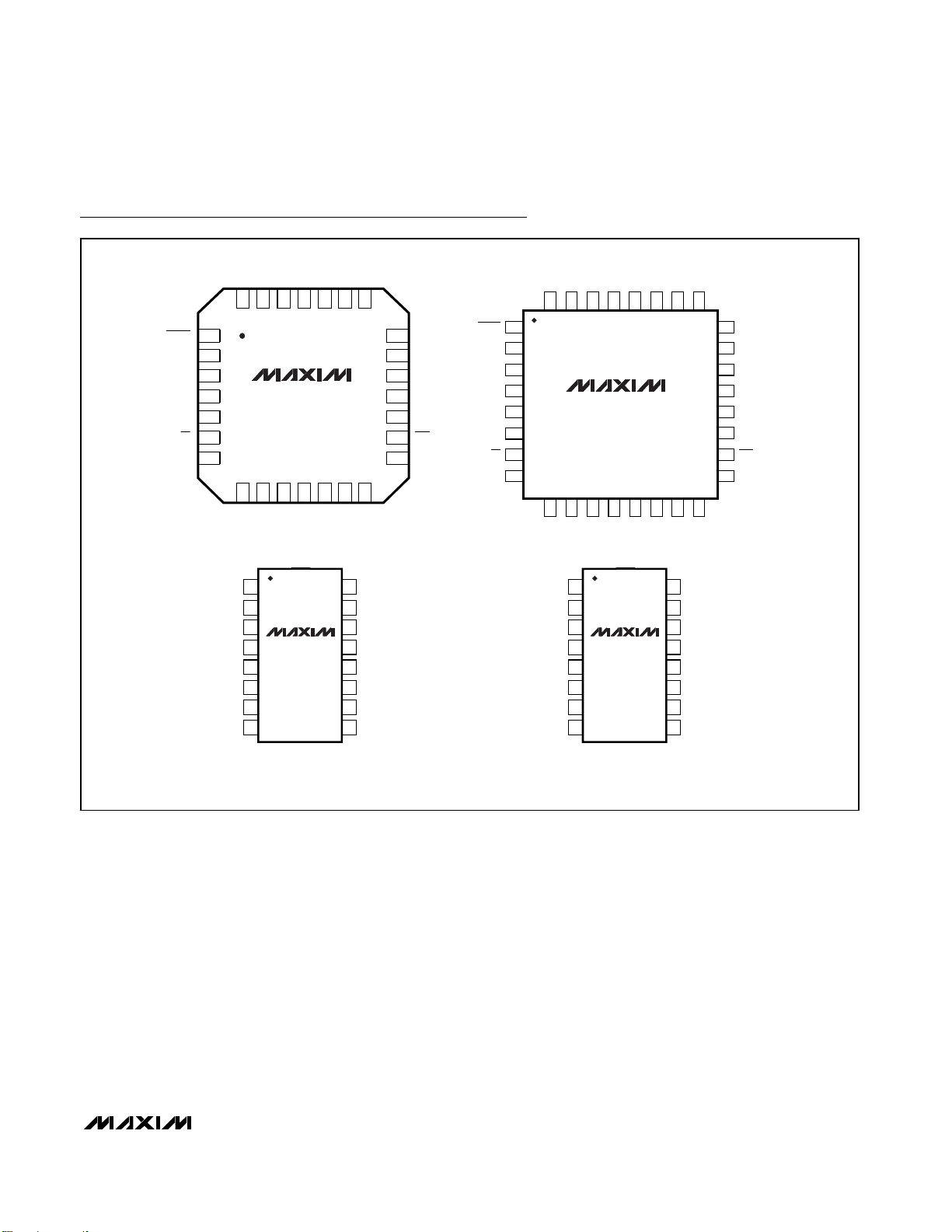
The MAX3286/MAX3296 are available in a compact, 5mm
✕
5mm, 28-pin QFN or thin QFN package; a 5mm ✕5mm,
32-pin TQFP package; or in die form. The MAX3287/
MAX3288/MAX3289 and MAX3297/MAX3298/MAX3299
are available in a 16-pin TSSOP-EP package.
Applications
Gigabit Ethernet Optical Transmitter
Fibre Channel Optical Transmitter
ATM LAN Optical Transmitter
Features
♦ 7ps Deterministic Jitter (MAX3296)
22ps Deterministic Jitter (MAX3286)
♦ +3.0V to +5.5V Supply Voltage
♦ Selectable Laser Pinning (Common Cathode or
Common Anode) (MAX3286/MAX3296)
♦ 30mA Laser Modulation Current
♦ Temperature Compensation of Modulation Current
♦ Automatic Laser Power Control or Constant
Bias Current
♦ Integrated Safety Circuits
♦ Power-On Reset Signal
♦ QFN and Thin QFN Packages Available
MAX3286–MAX3289/MAX3296–MAX3299
3.0V
to
5.5V, 1.25Gbps/2.5Gbps
LAN Laser Drivers
________________________________________________________________ Maxim Integrated Products 1
19-1550; Rev 6; 11/04
Ordering Information continued at end of data sheet.
Ordering Information
Typical Application Circuits and Selector Guide appear at
end of data sheet.
*Exposed pad is connected to GND.
Pin Configurations continued at end of data sheet.
PART TEMP RANGE PIN-PACKAGE
MAX3286CTI+ 0°C to +70°C
28 Thin QFN
(5mm x 5mm)****
MAX3286CGI 0°C to +70°C
28 QFN
(5mm x 5mm)***
MAX3286CHJ 0°C to +70°C
32 TQFP
(5mm x 5mm)
28
272625
242322
TC
MODSET
V
CC
OUT-
OUT+
VCCV
CC
8
9
10
11
121314
FLTDLY
LV
V
CC
IN+
IN-
GND
REF
15
16
17
18
19
20
21
POL
POL
MD
MON
GND
SHDNDRV
BIASDRV
7
6
5
4
3
2
1
PORDLY
EN
EN
GND
POR
FAULT
FAULT
MAX3286
MAX3296
THIN QFN*
TOP VIEW
+
Pin Configurations
For pricing, delivery, and ordering information, please contact Maxim/Dallas Direct! at
1-888-629-4642, or visit Maxim’s website at www.maxim-ic.com.
*Dice are designed to operate from TJ= 0°C to +110°C, but
are tested and guaranteed only at TA= +25°C.
**Exposed pad.
***Package Code: G2855-1
****Package Code: T2855-7
+Denotes Lead-Free Package.
Page 2
MAX3286–MAX3289/MAX3296–MAX3299
3.0V to 5.5V, 1.25Gbps/2.5Gbps
LAN Laser Drivers
2 _______________________________________________________________________________________
ABSOLUTE MAXIMUM RATINGS
ELECTRICAL CHARACTERISTICS
(VCC= +3.0V to +5.5V, TA= 0°C to +70°C, unless otherwise noted. Typical values are at VCC= +3.3V, RTC= open and TA= +25°C;
see Figure 1a.)
Stresses beyond those listed under “Absolute Maximum Ratings” may cause permanent damage to the device. These are stress ratings only, and functional
operation of the device at these or any other conditions beyond those indicated in the operational sections of the specifications is not implied. Exposure to
absolute maximum rating conditions for extended periods may affect device reliability.
Supply Voltage at VCC..........................................-0.5V to +7.0V
Voltage at
EN, EN, PORDLY, FLTDLY, LV, IN+, IN-,
REF, POL, POL, MD, MON, BIASDRV,
MODSET, TC.......................................................-0.5V to (V
CC
+ 0.5V)
Voltage at OUT+, OUT-.........................(V
CC
- 2V) to (VCC+ 2V)
Current into FAULT, FAULT, POR, SHDNDRV....-1mA to +25mA
Current into OUT+, OUT- ....................................................60mA
Continuous Power Dissipation (T
A
= +70°C)
32-Pin TQFP (derate 14.3mW/°C above +70°C).........1100mW
28-Pin QFN and 28-Pin Thin QFN
(derate 28.7mW/°C above +70°C)..............................2300mW
16-Pin TSSOP (derate 27mW/°C above +70°C) .........2162mW
Operating Temperature Range...............................0°C to +70°C
Operating Junction Temperature Range ..............0°C to +150°C
Processing Temperature (die) .........................................+400°C
Storage Temperature Range .............................-55°C to +150°C
Lead Temperature (soldering, 10s) .................................+300°C
0 ≤ V
PIN
≤ V
CC
Total differential signal, peak-to-peak, Figure 1a
LV = open
Figure 1a, R
MOD
= 1.82kΩ
LV = GND
V
MON
= V
CC
I
REF
≤ 2mA, MON = V
CC
FAULT = low, V
BIASDRV
≥ 0.6V
Normal operation (FAULT = low)
EN = GND
IOH= -100µA
Common-cathode configuration
IOL= 1mA
APC loop is closed
CONDITIONS
V
MD
+ 5% V
MD
+ 20%MD High Fault Threshold
V2.95REF Fault Threshold
mV150POR Hysteresis
2.65 3.00
V
3.9 4.5
POR Threshold
µA0.44 6MON Input Current
µA-2 +0.16 +2MD Input Current
V
0.4 1.2
V1.55 1.7 1.85V
MD
MD Nominal Voltage
µA-100 +100TTL Input Current
mV200 1660V
ID
mA52 75I
CC
Supply Current
Data Input Voltage Swing
V2.45 2.65 2.85REF Voltage
mA0.8BIASDRV Current Sink
µA-1 +1BIASDRV Current, Shutdown
V2V
IH
TTL Input High Voltage
V0.8V
IL
TTL Input Low Voltage
V2.4V
OH
FAULT, FAULT Output High
Voltage
V0.4V
OL
FAULT, FAULT Output Low
Voltage
UNITSMIN TYP MAXSYMBOLPARAMETER
Common-anode configuration 2VCC- 0.8
MD Voltage During Fault
V
MD
- 20% V
MD
- 5%MD Low Fault Threshold
MAX3286/MAX3288/MAX3296/MAX3298
mV
VCC- V
CC -
600 480
MON Fault Threshold
V
0.9MODSET, TC Fault Threshold
FAULT = low, V
BIASDRV
≤ VCC- 1V 0.8BIASDRV Current Source
BIAS GENERATOR (Note 1)
POWER-ON RESET
FAULT DETECTION
mA
Page 3
MAX3286–MAX3289/MAX3296–MAX3299
3.0V to 5.5V, 1.25Gbps/2.5Gbps
LAN Laser Drivers
_______________________________________________________________________________________ 3
ELECTRICAL CHARACTERISTICS (continued)
(VCC= +3.0V to +5.5V, TA= 0°C to +70°C, unless otherwise noted. Typical values are at VCC= +3.3V, RTC= open and TA= +25°C;
see Figure 1a.)
I
SHDNDRV
= 15mA, FAULT not asserted
I
SHDNDRV
= 10µA, FAULT asserted
MAX3296 series
MAX3286 series
I
SHDNDRV
= 1mA, FAULT not asserted
MAX3286 series
MAX3296 series
Tempco = max, R
MOD
= open; Figure 5
CONDITIONS
620 800 980Differential Input Resistance
4000
Modulation-Current
Temperature Coefficient
0V
CC
- 1.2
VCC- 0.4
Voltage at SHDNDRV
15 200Shutdown Modulation Current
24
28
RMSRandom Jitter (Note 3)
0V
CC
- 2.4
1.25
Data Rate
UNITS
MIN TYP MAXSYMBOL
PARAMETER
2
Minimum Laser Modulation
Current
MAX3286 series
20% to 80%
Modulation-Current Edge
Speed
MAX3296 series
R
MOD
= 13kΩ
(I
MOD
= 5mA)
MAX3286 series
46 65
Deterministic Jitter (Note 2)
R
MOD
= 4.1kΩ
(I
MOD
= 15mA)
R
MOD
= 1.9kΩ
(I
MOD
= 30mA)
22 35
R
MOD
= 13kΩ
(I
MOD
= 5mA)
MAX3296 series
14 35
R
MOD
= 4.1kΩ
(I
MOD
= 15mA)
822
R
MOD
= 1.9kΩ
(I
MOD
= 30mA)
720
C
PORDLY
= 0.01µF,
MAX3286/MAX3296 only
3 5.5
(Note 4)
Glitch Rejection at MD 10 20
22t
FAULT
Fault Time
SHUTDOWN
LASER MODULATOR
50Tempco = min, RTC= open; Figure 5
R
MOD
= 13kΩ (I
MOD
= 5mA) -15 +15
Single ended 42 50 58Output Resistance
LASER SAFETY CIRCUIT
PORDLY = open 0.3 1.25
t
PORDLY
POR Delay
V
CC
- 0.3
Input Bias Voltage
RL≤ 25Ω 30
Maximum Laser Modulation
Current
R
MOD
= 1.9kΩ (I
MOD
= 30mA) -10 +10
Tolerance of Modulation Current
V
mA
mA
%
ps
ps
µA
ppm/°C
Ω
Ω
V
µs
ms
µs
µs
29 45
ps
90 150
130 220
2.5
Gbps
Page 4
MAX3286–MAX3289/MAX3296–MAX3299
3.0V to 5.5V, 1.25Gbps/2.5Gbps
LAN Laser Drivers
4 _______________________________________________________________________________________
Typical Operating Characteristics
(TA = +25°C, unless otherwise noted.)
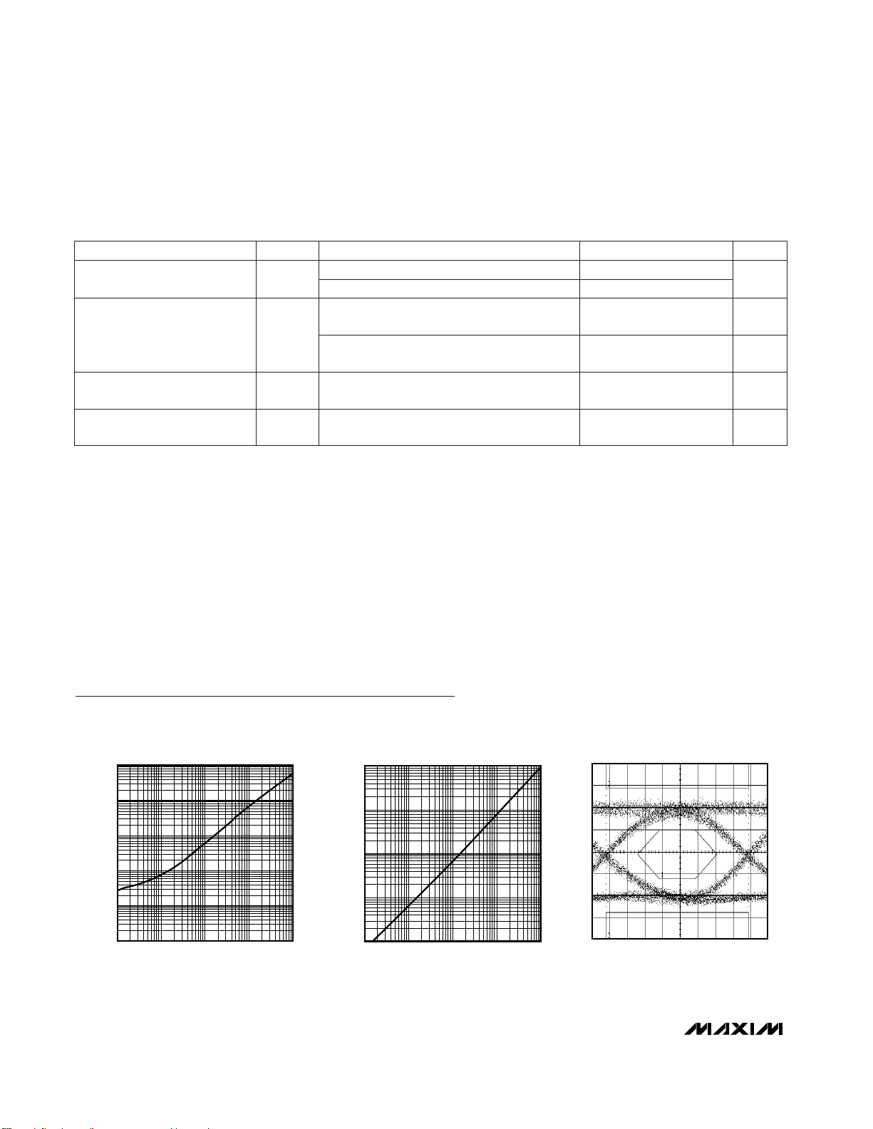
POR DELAY vs. C
PORDLY
MAX3286 toc01
CAPACITANCE (pF)
DELAY (µs)
10,000
100,000
1
10
100
1000
100 1000 10,00010 100,000
FLTDLY DURATION vs. C
FLTDLY
MAX3286 toc02
CAPACITANCE (pF)
DELAY (µs)
10,000
1
10
100
1000
100 1000 10,000101
Note 1: Common-anode configuration refers to a configuration where POL = GND, POL = VCC, and an NPN device is used to set
the laser bias current. Common-cathode configuration refers to a configuration where POL = V
CC
, POL = GND, and a PNP
device is used to set the laser bias current.
Note 2: Deterministic jitter measured with a repeating K28.5 bit pattern 00111110101100000101. Deterministic jitter is the peak-to-
peak deviation from the ideal time crossings per ANSI X3.230, Annex A.
Note 3: For Fibre Channel and Gigabit Ethernet applications, the peak-to-peak random jitter is 14.1 times the RMS jitter.
Note 4: Delay from a fault on MD until FAULT is asserted high.
ELECTRICAL CHARACTERISTICS (continued)
(VCC= +3.0V to +5.5V, TA= 0°C to +70°C, unless otherwise noted. Typical values are at VCC= +3.3V, RTC= open and TA= +25°C;
see Figure 1a.)
MAX3286/MAX3296 only, Figure 1b,
C
FLTDLY
= open
C
FLTDLY
= 270pF
C
FLTDLY
= 0
MAX3286/MAX3296 only, Figure 1b
MAX3286/MAX3296 only, Figure 1b
CONDITIONS
ns610
t
EN_RESET
EN or EN Minimum Pulse Width
Required to Reset a Latched
Fault
100 140
µs
0.2 1
t
FLTDLY
FLTDLY Duration
µs3.5 5.5t
SHUTDN
SHDNDRV Asserted after EN =
Low or EN = High
µs12t
RESET
FAULT Reset after EN, EN, or
POR Transition
UNITSMIN TYP MAXSYMBOLPARAMETER
MAX3286/MAX3296 only, Figure 1b,
C
FLTDLY
= 0.01µF
6 µs
EYE DIAGRAM
50ps/div
2.5Gbps, 1310nm LASER, 27 - 1 PRBS, I
MOD
MAX3286 toc03
= 15mA
Page 5
MAX3286–MAX3289/MAX3296–MAX3299
3.0V to 5.5V, 1.25Gbps/2.5Gbps
LAN Laser Drivers
_______________________________________________________________________________________ 5
Pin Description
Typical Operating Characteristics (continued)
(TA = +25°C, unless otherwise noted.)
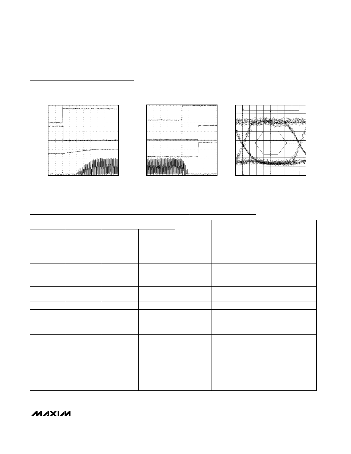
EN STARTUP
(COMMON-ANODE CONFIGURATION)
MAX3286 toc04
EN
OPTICAL
OUTPUT
BIASDRV
FAULT
5µs/div
MD SHUTDOWN
MAX3286 toc05
MD
OPTICAL
OUTPUT
SHDNDRV
FAULT
10µs/div
EYE DIAGRAM
MAX3286 toc06
100ps/div
1.25Gbps, 1310nm LASER, 2
7
- 1 PRBS, I
mod
= 15mA
PIN
QFN/
THIN QFN
MAX3286
MAX3296
TQFP
MAX3286
MAX3296
TSSOP-EP
MAX3287
MAX3297
MAX3289
MAX3299
TSSOP-EP
MAX3288
MAX3298
NAME FUNCTION
11——FAULT Inverting Fault Indicator. See Table 1.
—2, 16, 19 — — N.C. No Connect
23——FAULT Noninverting Fault Indicator. See Table 1.
34——POR
Power-On Reset. POR is a TTL-compatible
output. See Figure 14.
4, 13, 19
1, 6 1, 6 GND Ground
56——EN
Enable TTL Input. The laser output is enabled
only when EN is high and EN is low. If EN is
left unconnected, the laser is disabled.
67——EN
Inverting Enable TTL Input. The laser output
is enabled only when EN is low or grounded
and EN is high. If EN is left unconnected, the
laser is disabled.
78——PORDLY
Power-On Reset Delay. To extend the delay
for the power-on reset circuit, connect a
capacitor to PORDLY. See the Design
Procedure section.
5, 14, 22, 30
Page 6
MAX3286–MAX3289/MAX3296–MAX3299
3.0V to 5.5V, 1.25Gbps/2.5Gbps
LAN Laser Drivers
6 _______________________________________________________________________________________
Pin Description (continued)
PIN
QFN/
THIN QFN
MAX3286
MAX3296
TQFP
MAX3286
MAX3296
TSSOP-EP
MAX3287
MAX3297
MAX3289
MAX3299
TSSOP-EP
MAX3288
MAX3298
NAME FUNCTION
8922FLTDLY
Fault Delay Input. Determines the delay of
the FAULT and FAULT outputs. A capacitor
attached to FLTDLY ensures proper startup
(see the Typical Operating Characteristics) .
FLTDLY = GND: holds FAULT low and
FAULT high. When FLTDLY = GND, EN =
high, EN = low, and V
CC
is within the
operational range, the safety circuitry is
inactive.
910——LV
Low-Voltage Operation. Connect to GND for
4.5V to 5.5V operation. Leave open for 3.0V
to 5.5V operation (Table 2).
10, 22, 23,
26
11, 25, 26,
29
3, 11, 14 3, 11, 14 V
CC
Supply Voltage
11 12 4 4 IN+ Noninverting Data Input
12 13 5 5 IN- Inverting Data Input
14 15 7 7 REF
Reference Voltage. A resistor connected at
REF to MD determines the laser power when
APC is used with common-cathode lasers.
15 17 — — POL
Polarity Input. POL is used for programming
the laser-pinning polarity (Table 4).
16 18 — — POL
Inverting Polarity Input. POL is used for
programming the laser-pinning polarity
(Table 4).
17 20 8 8 MD
Monitor Diode Connection. MD is used for
automatic power control.
18 21 — 9 MON
Laser Bias Current Monitor. Used for
programming laser bias current in VCSEL
applications.
20 23 9 — SHDNDRV
Shutdown Driver Output. Provides a
redundant laser shutdown.
21 24 10 10 BIASDRV
Bias-Controlling Transistor Driver. Connects
to the base of an external PNP or NPN
transistor.
Page 7
MAX3286–MAX3289/MAX3296–MAX3299
3.0V to 5.5V, 1.25Gbps/2.5Gbps
LAN Laser Drivers
_______________________________________________________________________________________ 7
MD
FAULT CONDITION
V
CC
VMD> 1.15 ✕V
MD(nom)
,
V
MD
< 0.85 ✕V
MD(nom)
LV = GND and VCC< 4.5V
REF
EN and EN
V
REF
> 2.95V
PIN
POL and POL
EN = low or open, EN = high or open
POL = POL
MON V
MON
< VCC- 540mV
Table 1. Typical Fault Conditions
>4.5Grounded
>3.0Open
OPERATING VOLTAGE
RANGE (V)
LV
Table 2. LV Operating Range
MODSET
and TC
V
MODSET
and VTC≤ 0.8V
Pin Description (continued)
PIN
QFN/
THIN QFN
MAX3286
MAX3296
TQFP
MAX3286
MAX3296
TSSOP-EP
MAX3287
MAX3297
MAX3289
MAX3299
TSSOP-EP
MAX3288
MAX3298
NAME FUNCTION
24 27 12 12 OUT+
Modulation-Current Output. See the Typical
Application Circuits.
25 28 13 13 OUT-
Modulation-Current Output. See the Typical
Application Circuits.
27 31 15 15 MODSET
Modulation-Current Set. The resistor at
MODSET programs the temperature-stable
component of the laser modulation current.
28 32 16 16 TC
Temperature-Compensation Set. The resistor
at TC programs the temperature-increasing
component of the laser modulation current.
EP — EP EP
Exposed
Pad
Ground. This must be soldered to the circuit
board ground for proper thermal
performance. See Layout Considerations.
Page 8
MAX3286–MAX3289/MAX3296–MAX3299
3.0V to 5.5V, 1.25Gbps/2.5Gbps
LAN Laser Drivers
8 _______________________________________________________________________________________
MODULATION
CONTROL
MODSET
TC
L = 3.9nH
L = 3.9nH
R
L
= 25Ω
BIASDRV
LASER
EQUIVALENT
LOAD
(OPEN)
OUT- OUT+
FERRITE BEAD*
*MURATA
BLM11HA102
0.01µF
0.01µF
IN+
IN-
50Ω 50Ω
25Ω
R
L
R
MOD
V
CC
V
CC
V
CC
I
OUT
I
CC
V
CC
I
MOD
3/2
i
MOD
V
ID
VID = V
IN+ - VIN-
CURRENT
I
MOD
V
IN-
V
IN+
VOLTS
TIME
100mV
P-P
MIN
830mV
P-P
MAX
200mV
P-P
MIN
1660mV
P-P
MAX
DIFFERENTIAL INPUT
RESULTING SIGNAL
MAX3286
MAX3296
Figure 1a. Output Load for AC Specification
V
CC
POR
FAULT
FAULT ON MD RESET BY EN SHUTDOWN
BY EN
SHDNDRV
OPTICAL
OUT
EN
NOTE: TIMING IS NOT TO SCALE.
t
PORDLY
t
FAULT
t
RESET
t
SHUTDN
t
EN_RESET
Figure 1b. Fault Timing
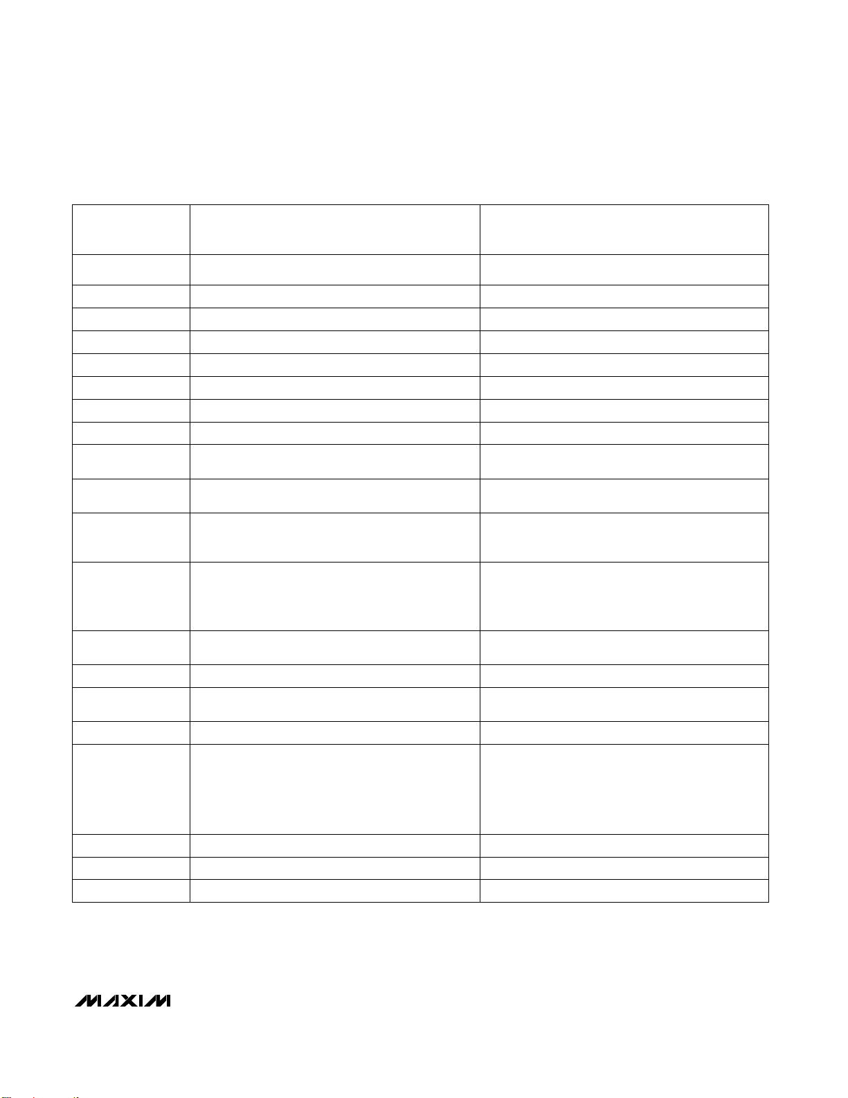
_______________Detailed Description
The MAX3286/MAX3296 series of laser drivers contain a
bias generator with APC, laser modulator, power-on reset
(POR) circuit, and safety circuitry (Figures 2a and 2b).
Bias Generator
Figure 3 shows the bias generator circuitry containing a
power-control amplifier, controlled reference voltage,
smooth-start circuit, and window comparator. The bias
generator combined with an external PNP or NPN transistor provides DC laser current to bias the laser in a lightemitting state. When there is a monitor diode (MD) in the
laser package, the APC circuitry adjusts the laser-bias
current to maintain average power over temperature and
changing laser properties. The MD input is connected to
Page 9
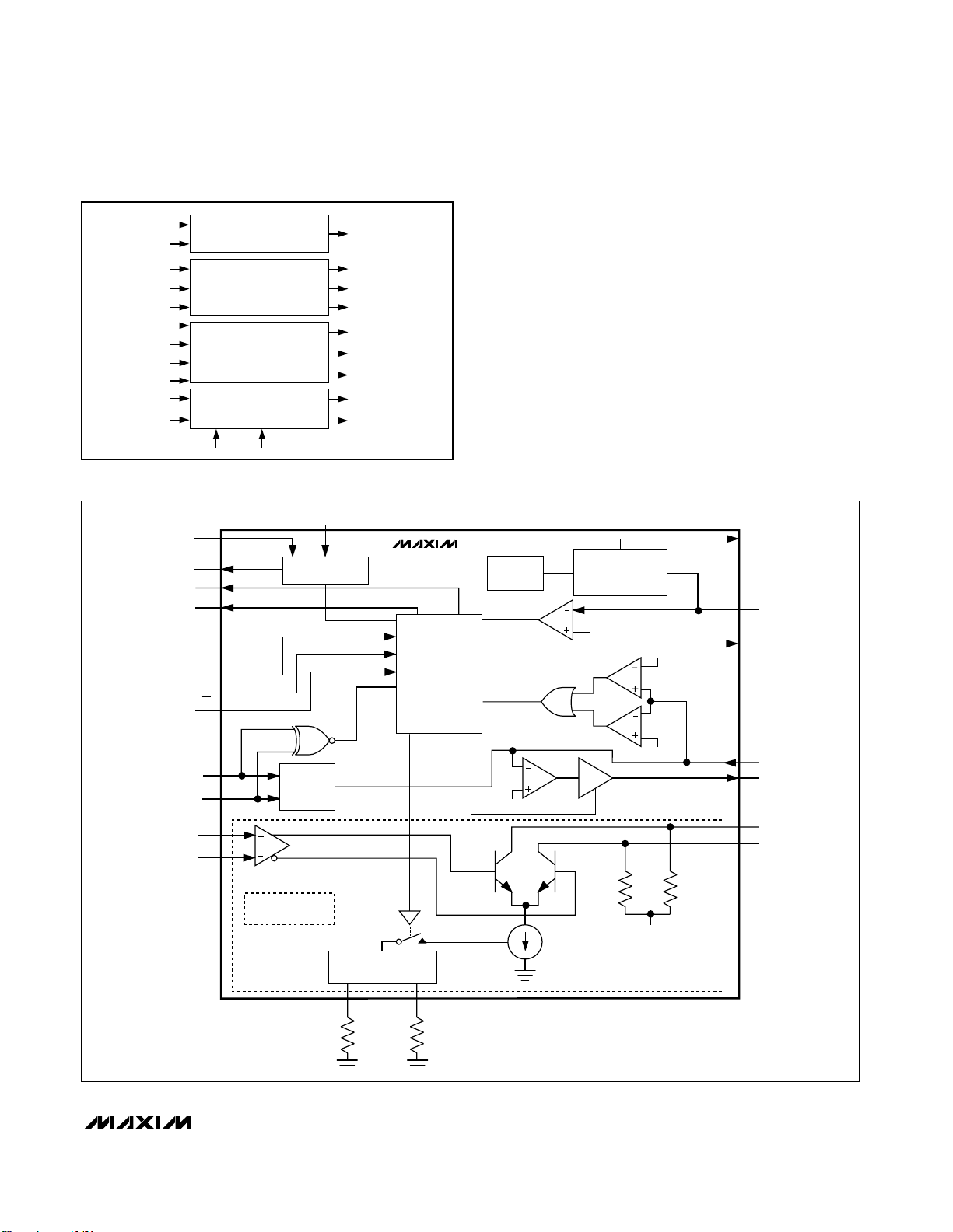
MAX3286–MAX3289/MAX3296–MAX3299
3.0V to 5.5V, 1.25Gbps/2.5Gbps
LAN Laser Drivers
_______________________________________________________________________________________ 9
SMOOTH-
START
IN+
IN-
TC MODSET
R
MOD
V
CC
R
TC
MON
SHDNDRV
REF
POR
PORDLY
POL
POL
FAULT
FAULT
FLTDLY
EN
EN
1.97V
LV
1.53V
+1.7V
50Ω 50Ω
CONTROLLED
REFERENCE
GENERATOR
LASER
MODULATOR
MODULATION CURRENT
GENERATOR
1.7V
REF
BIASDRV
MD
OUTOUT+
POR CIRCUIT
SAFETY
CIRCUITRY
INPUT BUFFER
VCC - 0.54V
MAX3286
MAX3296
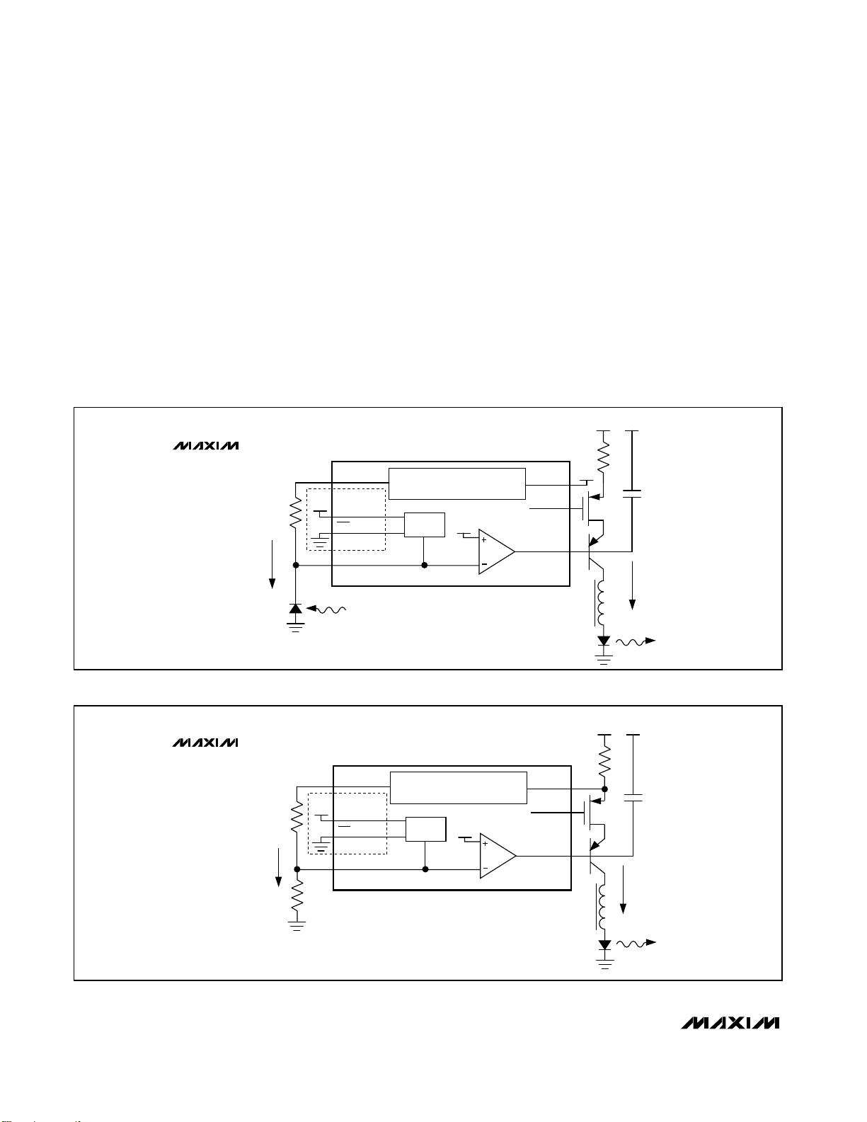
BIAS GENERATOR
Figure 2b. Laser Driver Functional Diagram
LASER
MODULATOR
POR CIRCUIT
SAFETY
BIAS GENERATOR
MODSET
TC
BIASDRV
MD
SHDNDRV
FAULT
FAULT
POR
LV
PORDLY
EN
EN
FLTDLY
POL
POL
MON
MD
OUT-
OUT+
REF
IN+
IN-
Figure 2a. Simplified Laser Driver Functional Diagram
the anode or cathode of a monitor photodiode or to a
resistor-divider, depending on the specific application
circuit. Three application circuits are supported:
common-cathode laser with photodiode, commoncathode laser without photodiode, and common-anode
laser with photodiode (as shown in the Design Procedure
section). The POL and POL inputs determine the laser
pinning (common cathode, common anode) (Table 4).
The smooth-start circuitry prevents current spikes to the
laser during power-up or enable; this ensures compliance
with safety requirements and extends the life of the laser.
The power-control amplifier drives an external transistor
to control the laser bias current. In a fault condition, the
power-control amplifier’s output is disabled (high
Page 10
MAX3286–MAX3289/MAX3296–MAX3299
3.0V to 5.5V, 1.25Gbps/2.5Gbps
LAN Laser Drivers
10 ______________________________________________________________________________________
impedance). This ensures that the PNP or NPN transistor
is turned off, removing the laser-bias current. (See the
Applications Information section.)
The REF pin provides a controlled reference voltage
dependent upon the voltage at MON. The voltage at REF
is V
REF
= 2.65 - 2.25(VCC- V
MON
). A resistor connected
at REF determines the laser power when APC is used
with common-cathode lasers. See the Design Procedure
section for information about setting the laser power.
Modulation Circuitry
The modulator circuitry consists of an input buffer, current
generator, and high-speed current switch (Figure 4). The
modulator drives up to 30mA of modulation current into
a 25Ω load.
Many of the modulator performance specifications
depend on the total modulator current (I
OUT
) (Figure 1a).
To ensure good driver performance, the voltage at
OUT+ and OUT- must not be less than VCC- 1V.
The amplitude of the modulation current is set with
resistors at the MODSET and temperature coefficient (TC)
pins. The resistor at MODSET (R
MOD
) programs the
temperature-stable portion of modulation current, while
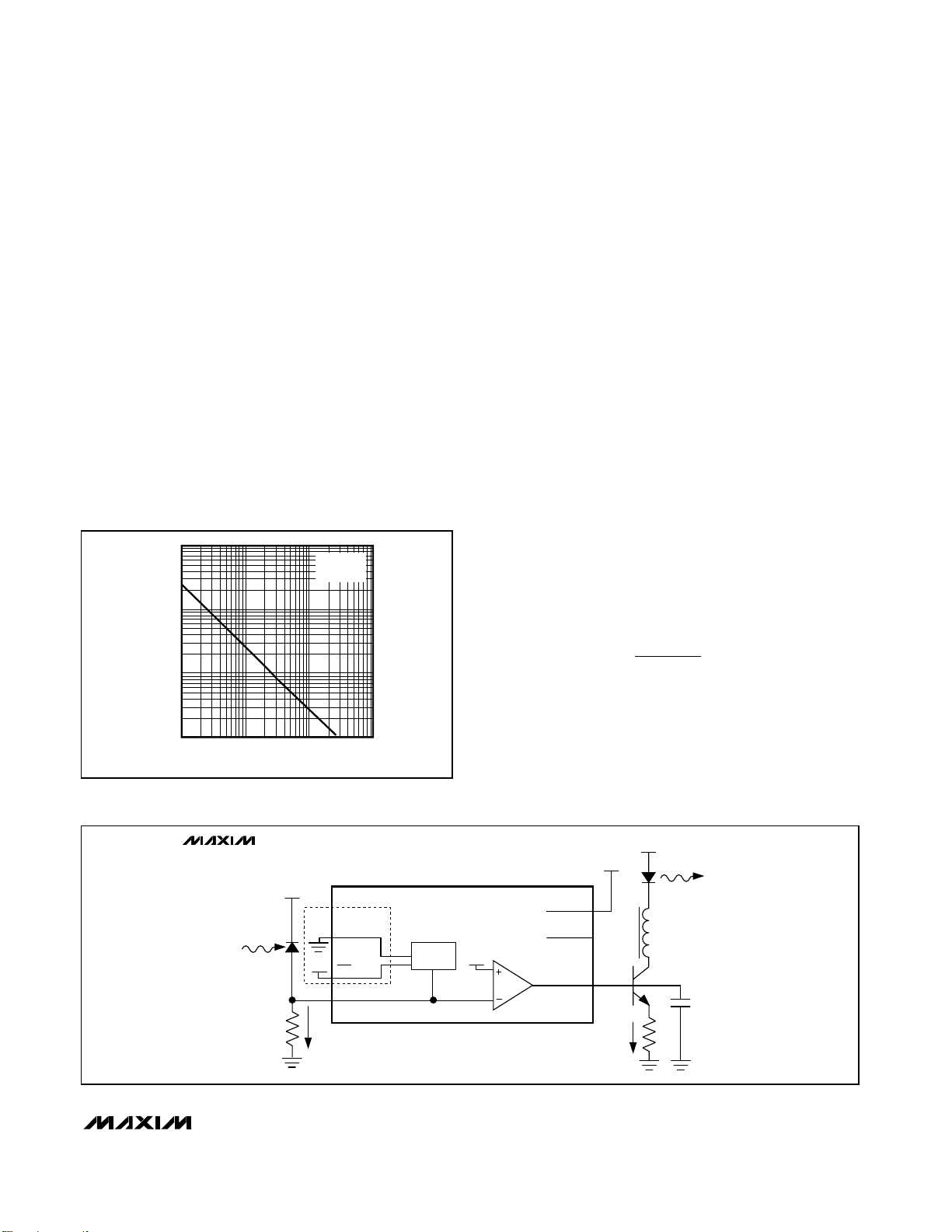
the resistor at TC (RTC) programs the temperatureincreasing portion of the modulation current. Figure 5
shows modulation current as a function of temperature
for two extremes: RTCis open (the modulation current
has zero temperature coefficient) and R
MOD
is open
(the modulation temperature coefficient is 4000ppm).
Intermediate tempco values of modulation current can
be obtained as described in the Design Procedure section. Table 3 is the RTCand R
MOD
selection table.
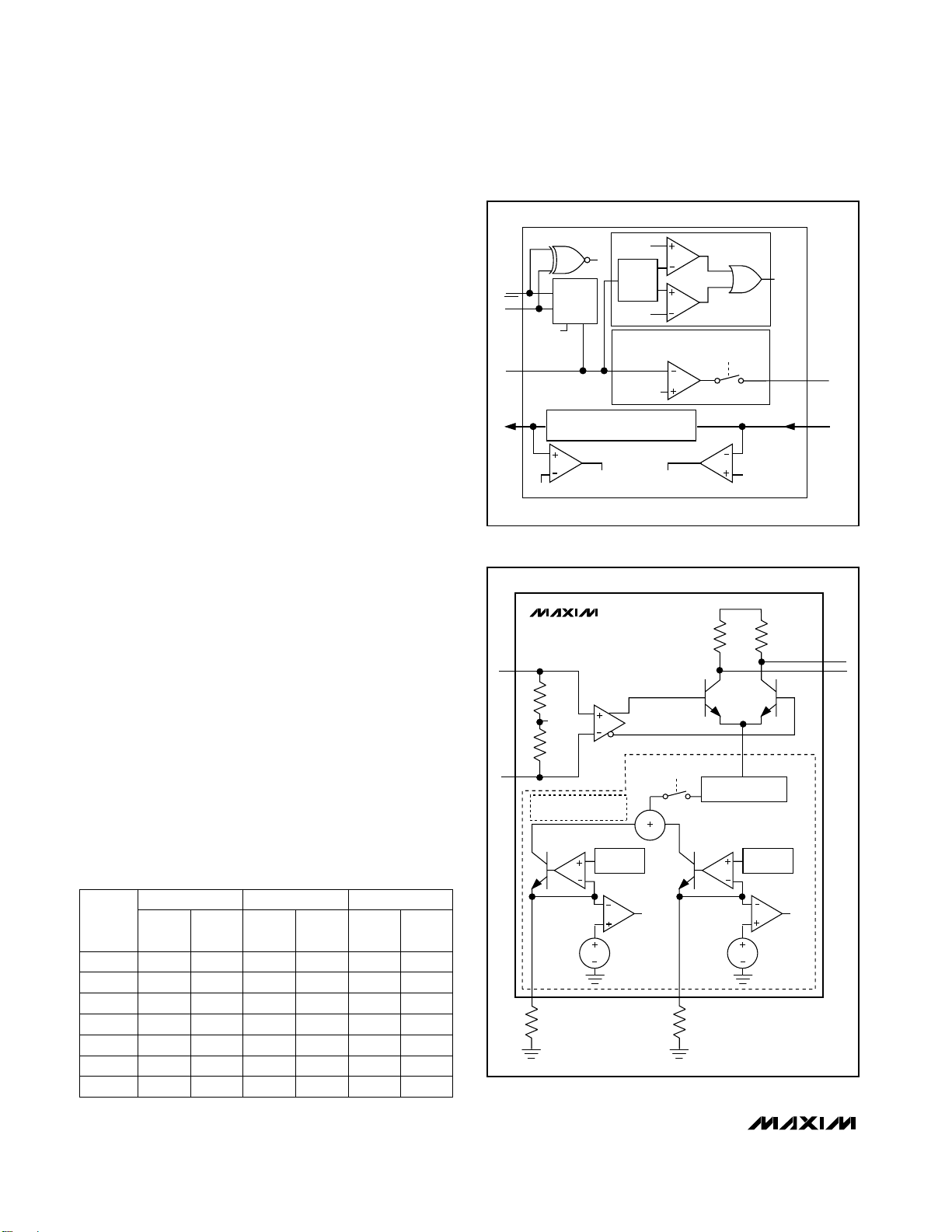
Safety Circuitry
The laser driver can be used with two popular safety
systems. APC maintains laser safety using local feedback. Safety features monitor laser driver operation and
SMOOTH-
START
POLARITY_FAULT
ENABLE
WINDOW
COMPARATOR
MD
FAULT
REF_FAULT MONITOR_FAULT
V
CC
- 540mV
BIASDRV
MON
POL
POL
MD
REF
POWER-
CONTROL
AMPLIFIER
+1.7V
CONTROLLED REFERENCE VOLTAGE
V
REF
= 2.65 - 2.25 (VCC - V
MON
)
+1.97V
2.95V
+1.53V
GLITCH
REJECT
ENABLE
Figure 3. Bias Generator Circuitry
V
CC
CURRENT
SWITCH
INPUT
BUFFER
OUT+
OUT-
IN+
IN-
50Ω 50Ω
400Ω
400Ω
V
CC
- 0.3V
CURRENT AMPLIFIER
4000ppm/°C
REFERENCE
ENABLE
0.8V
TC MODSET
R
TC
R
MOD
0.8V
TC_FAULT
MOD_FAULT
MODULATION CURRENT
GENERATOR
1.2V
REFERENCE
MAX3286
MAX3296
Figure 4. Laser Modulator Circuitry
53.61.69
R
MOD
(kΩ)
R
TC
(kΩ)
I
MOD
= 15mA
11.526.73500 162
R
MOD
(kΩ)
R
TC
(kΩ)
I
MOD
= 30mA
R
MOD
(kΩ)
I
MOD
= 5mA
3.65
R
TC
(kΩ)
TEMPCO
(ppm/°C)
8.063.16
11.32.49
18.72.0
20.04.122000 24.9
5.762500 16.2
9.533000
34.8
13.357.6
6.49
5.23
4.32
4.2213.3
5.116.49
6.194.32
80.62.26500 13.3
2.671000 40.2
3.241500
15.8
26.719.1
26.7
13.3
8.87
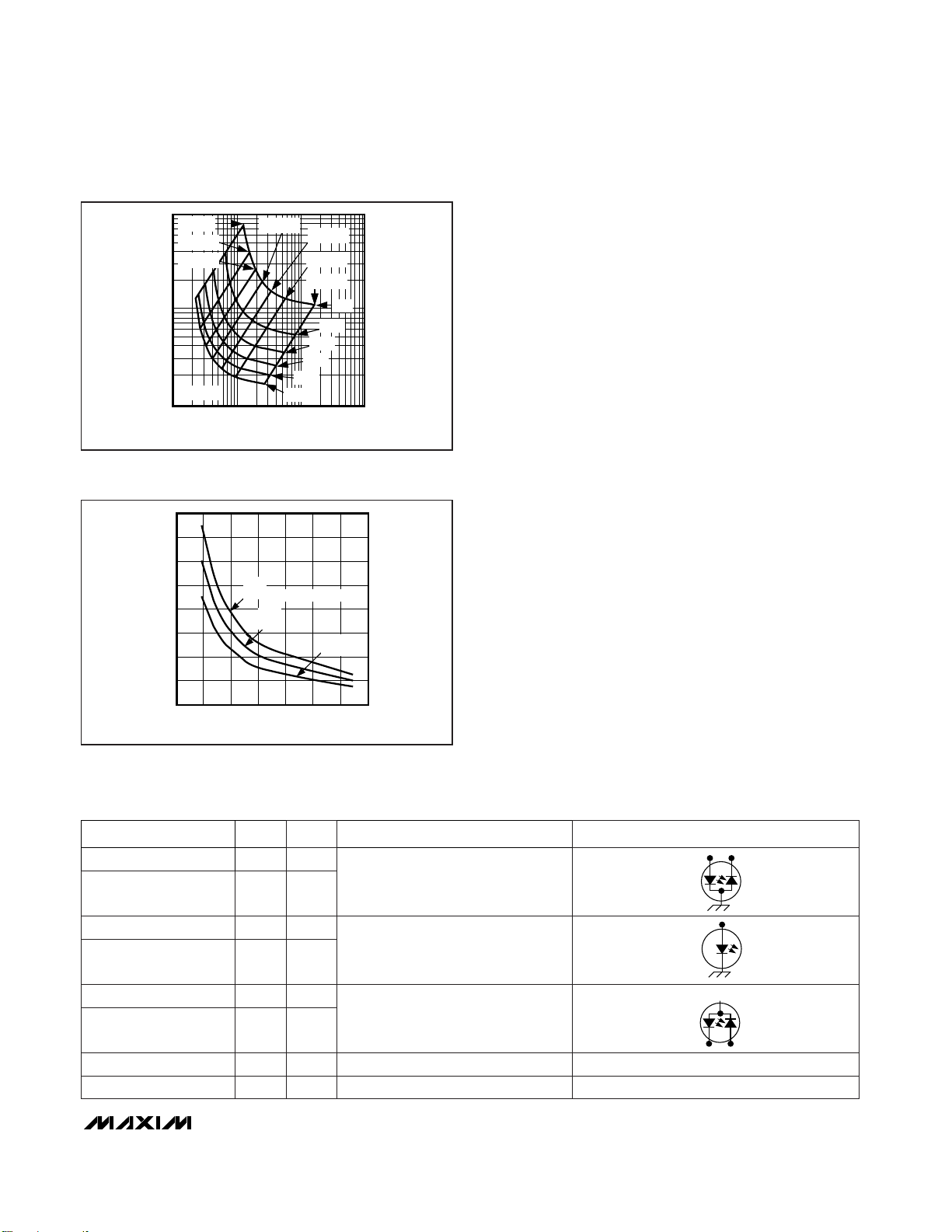
Table 3. RTCand R
MOD
Selection Table
Page 11
MAX3286–MAX3289/MAX3296–MAX3299
3.0V to 5.5V, 1.25Gbps/2.5Gbps
LAN Laser Drivers
______________________________________________________________________________________ 11
force a shutdown if a fault is detected. The shutdown
condition is latched until reset by a toggle of EN, EN, or
power.
Another safety system, open fiber control (OFC), uses
safety interlocks to prevent eye hazards. To accommodate the OFC standard, the MAX3286/MAX3296 series
provide dual enable inputs and dual fault outputs.
The safety circuitry contains fault detection, dual enable
inputs, latched fault outputs, and a pulse generator
(Figure 6).
Safety circuitry monitors the APC circuit to detect unsafe
levels of laser emission during single-point failures. A
single-point failure can be a short to VCCor GND or a
short between any two IC pins.
Pulse Generator
During startup, the laser does not emit light and the
APC loop is not closed, triggering a fault signal. To
allow startup, an internal fault-delay pulse disables the
safety system for a programmable period of time, allowing
the driver to begin operation. The length of the pulse is
determined by the capacitor connected at FLTDLY and
should be set 5 to 10 times longer than the APC time
constant. The internal safety features can be disabled
by connecting FLTDLY to GND. Note that EN must be
high, EN must be low, and VCCmust be in the operational range for laser operation.
Fault Detection
The MAX3286/MAX3296 series has extensive and comprehensive fault-detection features. All critical nodes
are monitored for safety faults, and any node voltage
that differs significantly from its expected value results
in a fault (Table 1). When a fault condition is detected,
the laser is shut down. See the Applications Information
section for more information on laser safety.
Shutdown
The laser drivers offer dual redundant bias shutdown
mechanisms. The SHDNDRV output drives an optional
external MOSFET semiconductor. The bias and modulation drivers have separate internal disable signals.
Latched Fault Output
Two complementary FAULT outputs are provided with
the MAX3286/MAX3296 series. In the event of a fault,
these outputs latch until one of three events occurs:
1) The power is switched off, then on.
V
CC
FLTDLY
FAULT
FAULT
SHDNDRV
(FROM POR CIRCUIT)
REF_FAULT
MONITOR_FAULT
MD_FAULT
POLARITY_FAULT
TC_FAULT
MOD_FAULT
EN
EN
ENABLE
QR
RESET
DOMINANT
FAULT
LATCH
FAULT
DETECTION
t
FLTDLY
PULSE GENERATOR
MAX3286
MAX3296
S
Figure 6. Simplified Safety Circuit Schematic
0.6
0.8
0.7
1.0
0.9
1.2
1.1
1.3
020304010 50 60 70 80 90 100 110
JUNCTION TEMPERATURE (°C)
I
MOD
/(I
MOD
AT+ 52°C)
RTC = OPEN
TEMPCO = 50ppm/°C
RTC ≥ 1.9kΩ
R
MOD
= OPEN
TEMPCO = 4000ppm/°C
Figure 5. Modulation Current vs. Temperature for Maximum
and Minimum Temperature Coefficient
Page 12
MAX3286–MAX3289/MAX3296–MAX3299
3.0V to 5.5V, 1.25Gbps/2.5Gbps
LAN Laser Drivers
12 ______________________________________________________________________________________
2) EN is switched low, then high.
3) EN is switched to high, then low.
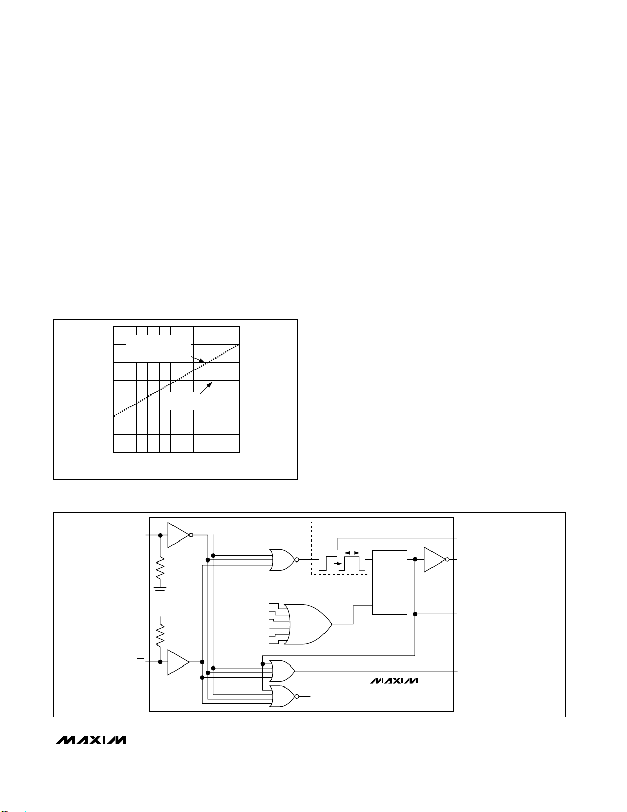
Power-On Reset (POR)
Figure 7 shows the POR circuit for the MAX3286/
MAX3296 series devices. A POR signal asserts low
when VCCis in the operating range. The voltage operating range is determined by the LV pin, as shown in
Table 2. POR contains an internal delay to reject noise
on VCCduring power-on or hot-plugging. The delay can
be extended by adding capacitance to the PORDLY
pin. The POR comparator includes hysteresis to improve
noise rejection. The laser driver is shut down while V
CC
is out of the operating range.
Design Procedure
Select Laser
Select a communications-grade laser with a rise time of
260ps or better for 1.25Gbps, or 130ps or better for
2.5Gbps applications. To obtain the MAX3286/
MAX3296’s AC specifications, the instantaneous output
voltage at OUT+ must remain above VCC- 1V at all
times. Select a high-efficiency laser that requires low
modulation current and generates low-voltage swing at
OUT+. Laser package inductance can be reduced by
trimming the leads. Typical package leads have inductance of 25nH/in (1nH/mm); this inductance causes a
larger voltage swing across the laser. A compensation filter network also can be used to reduce ringing, edge
speed, and voltage swing.
Programming the Modulation Current
Resistors at the MODSET and TC pins set the amplitude of the modulation current. The resistor R
MOD
sets
the temperature-stable portion of the modulation cur-
rent, while the resistor R
TC
sets the temperature-
increasing portion of the modulation current.
To determine the appropriate temperature coefficient
from the slope efficiency (α) of the laser, use the following
equation:
where α is the slope of the laser output power to the
laser current.
For example, suppose a laser has a slope efficiency
α25of 0.021mW/mA at +25°C, which reduces to
0.018mW/mA at +70°C. Using the above equation produces a laser tempco of -3175ppm/°C.
To obtain the desired modulation current and tempco
for the device, the following two equations can be used
to determine the required values of R
MOD
and RTC:
where tempco = -laser tempco.
Figure 8a shows a family of curves derived from these
equations. The straight diagonal lines depict constant
tempcos. The curved lines represent constant modulation currents. If no temperature compensation is
desired, Figure 8b displays a series of curves that
show laser modulation current with respect to R
MOD
for
different loads.
The following useful equations were used to derive
Figure 8a and the equations at the beginning of this
section. The first assumes RL = 25Ω.
Programming the Bias Current/APC
Three application circuits are described below: common-cathode laser with photodiode, common-cathode
laser without photodiode, and common-anode laser
III
tempco C C A
MOD C MOD C MOD C() () ()
()(–)
70 25 25
70 25
°°°
=+
°°
[]
I
RR
TC
A
MOD
MOD TC
=×
+ Ω
+
+ Ω
×
+× °
()
[]
−
51
115
250
106
250
140 10 25
3
..
.–
R
R empco
empco
MOD
TC
=
+ Ω ×
− ×
−Ω
()
(. )
250 52
019 48
250
t
t
R
tempco I
TC
MOD
=
()
−Ω
021
250
.
Laser tempco =
−
° − °
°
[]
×
αα
α
70 25
25
6
70 25
10
()
/
CC
ppm C
V
CC
PORDLY
POR
1.2V
36kΩ
25kΩ
28kΩ
LV
VARIABLE
DELAY
BANDGAP
= 0.7s/µF C
PORDLY
MAX3286
MAX3296
Figure 7. Power-On Reset Circuit
Page 13
MAX3286–MAX3289/MAX3296–MAX3299
3.0V to 5.5V, 1.25Gbps/2.5Gbps
LAN Laser Drivers
______________________________________________________________________________________ 13
with photodiode. The POL and POL inputs determine
the laser pinning (common cathode, common anode)
and affect the smooth-start circuits (Table 4).
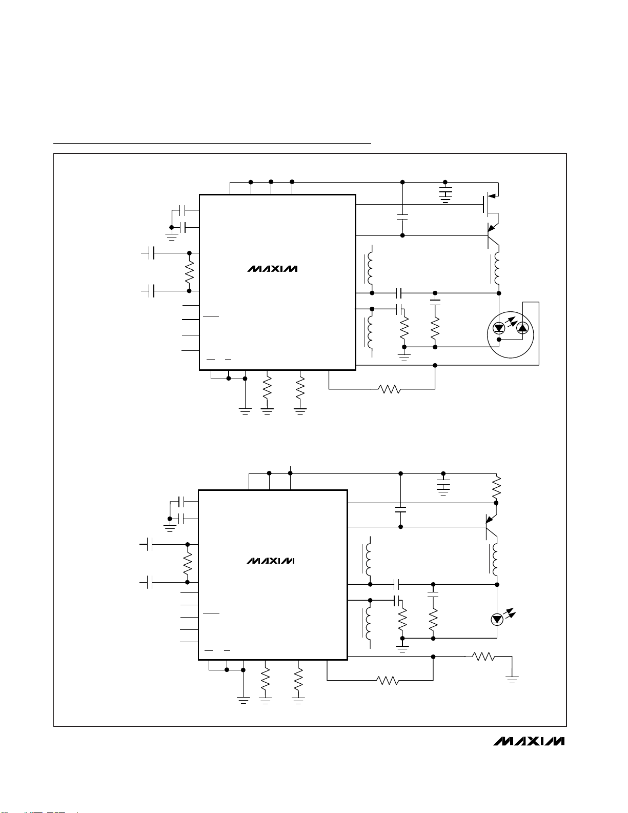
Common Cathode with Photodiode
(Optical Feedback)
In the common cathode with photodiode configuration,
a servo control loop is formed by external PNP Q1, the
laser diode, the monitor diode, R
SET
, and the powercontrol amplifier (Figure 9). The voltage at MD is stabilized to 1.7V. The monitor photodiode current (I
D
) is set
by (V
REF
- VMD) / R
SET
= 0.95 / R
SET
. Determine the
desired monitor current (ID), then select R
SET
= 0.95 / ID.
The APC loop is compensated by C
BIASDRV
. A capacitor
must be placed from BIASDRV to VCCto ensure lownoise operation and to reject power-supply noise. The
time constant governs how quickly the laser bias current
reacts to a change in the average total laser current
(I
BIASDRV
+ I
MOD
). A capacitance of 0.1µF is sufficient
to obtain a loop time constant in excess of 1µs, provided that R
DEG
is chosen appropriately. Resistor R
DEG
might be necessary to ensure the APC loop’s stability
when low bias currents are desired.
The voltage across R
DEG should not be larger than
250mV at maximum bias current.
The discrete components used with the common cath-
ode with photodiode configuration are:
R
SET
= 0.95 / I
D
C
BIASDRV
= 0.1µF (typ)
R
DEG
= 0.25 / I
BIAS(MAX)
POL DESCRIPTION
MAX3286/MAX3296 V
CC
Common cathode with
photodiode
DEVICE
Table 4. POL Pin Setup for Each Laser Configuration Type
POL
GND
LASER PINNING
MAX3287/MAX3297 — —
MAX3286/MAX3296 V
CC
Common cathode without
photodiode
MAX3288/MAX3298 —
GND
—
MAX3286/MAX3296 GND
Common anode with
photodiode
MAX3289/MAX3299 —
V
CC
—
MAX3286/MAX3296 V
CC
V
CC
Not allowed; fault occurs —
MAX3286/MAX3296 GND GND Not allowed; fault occurs —
Figure 8a. RTCvs. R
MOD
for Various Conditions
0
10
5
20
15
35
30
25
40
04268101214
R
MOD
(kΩ)
LASER MODULATION CURRENT (i
MOD
) (mA)
NOTE: RTC = OPEN
10Ω
LOAD
25Ω
LOAD
50Ω
LOAD
Figure 8b. Laser-Modulation Current vs. R
MOD
1000
(kΩ)
10
TC
R
1
500ppm
1000ppm
1500ppm
RL = 25Ω
1 100 1000
2000ppm
25mA
30mA
10
R
(kΩ)
MOD
2500ppm
3000ppm
3500ppm
10mA
15mA
20mA
5mA
V
CC
Page 14
MAX3286–MAX3289/MAX3296–MAX3299
3.0V to 5.5V, 1.25Gbps/2.5Gbps
LAN Laser Drivers
Q1 = general-purpose PNP, β >100, ft> 5MHz
B1 = ferrite bead (see Bias Filter section)
M1 = general-purpose PMOS device (optional)
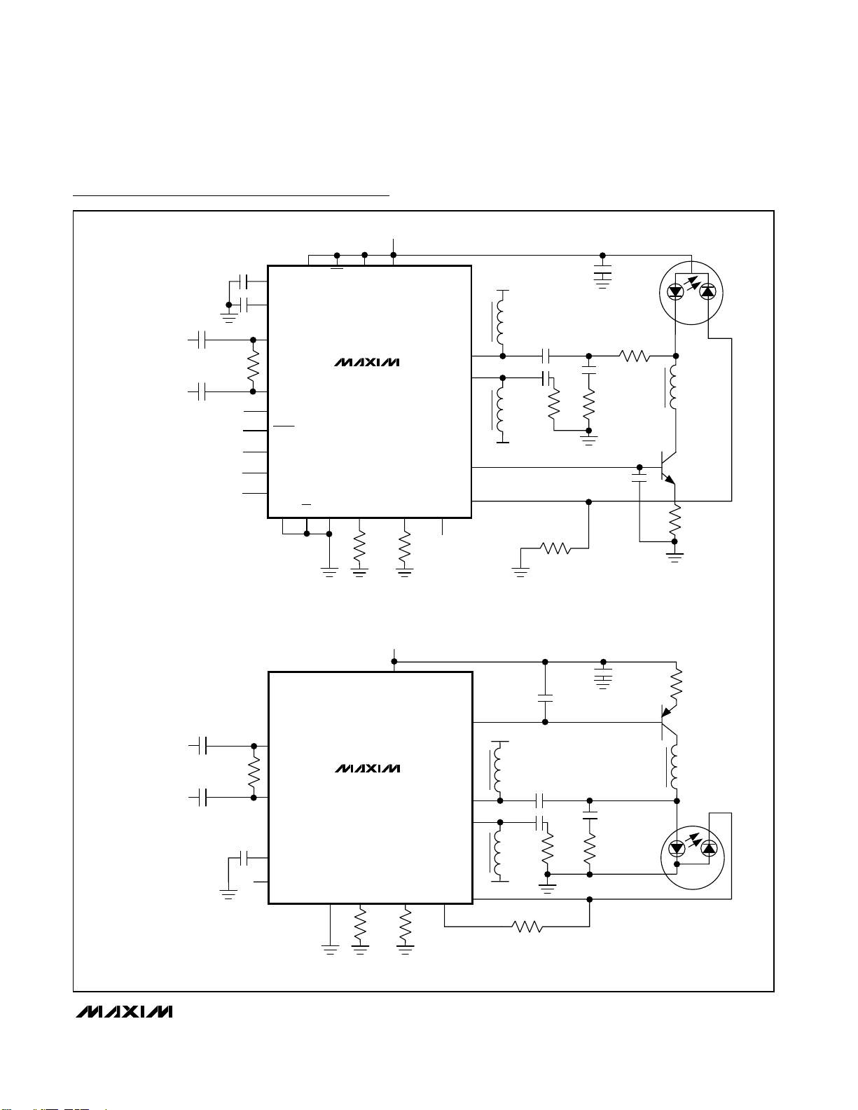
Common Cathode with Current Feedback
In the common-cathode configuration with current feedback, a servo control loop is formed by an external PNP
transistor (Q1), R
MON
, the controlled-reference voltage
block, R
SET
, RMD, and the power-control amplifier
(Figure 10). The voltage at MD is stabilized to 1.7V. The
voltage at MON is set by the resistors R
SET
and RMD.
As in the short-wavelength configuration, a 0.1µF
C
BIASDRV
connected between BIASDRV and VCCis
sufficient to obtain an approximate 1µs APC loop time
constant. This improves power-supply noise rejection.
To select the external components:
1) Determine the required laser bias current
I
BIAS
= ITH+ I
MOD / 2
2) Select RMDand R
SET
.
Maxim recommends R
SET
= 1kΩ, RMD= 5kΩ, which
results in VCC- V
MON
≈ 250mV.
3) Select R
MON
where R
MON
= 250mV / I
BIAS
, assuming
R
SET
= 1kΩ and RMD= 5kΩ.
V
CC
V
CC
R
DEG
V
CC
CONTROLLED REFERENCE VOLTAGE
V
REF
= 2.65V
REF
ONLY
MAX3286/96
SHDNDRV
C
BIASDRV
BIASDRV
MON
M1
Q1
POL
MD
POWER-CONTROL
AMPLIFIER
LASER
I
BIAS
PHOTO
DIODE
I
D
FERRITE
BEAD
B1
1.7V
SMOOTH-
START
V
CC
R
SET
POL
MAX3286
MAX3287
MAX3296
MAX3297
Figure 9. Common-Cathode Laser with Photodiode
V
CC
R
MON
V
CC
CONTROLLED REFERENCE VOLTAGE
V
REF
= 2.65V - 2.25V (VCC - V
MON
)
REF
MAX3286/96
ONLY
SHDNDRV
C
BIASDRV
BIASDRV
MON
M1
Q1
POL
MD
POWER-CONTROL
AMPLIFIER
I
BIAS
I
D
FERRITE
BEAD
B1
1.7V
SMOOTH-
START
V
CC
R
SET
R
MD
POL
MAX3286
MAX3288
MAX3296
MAX3298
LASER
Figure 10. Common Cathode with Current Feedback (PNP Configuration)
14 ______________________________________________________________________________________
Page 15
______________________________________________________________________________________ 15
MAX3286–MAX3289/MAX3296–MAX3299
3.0V to 5.5V, 1.25Gbps/2.5Gbps
LAN Laser Drivers
V
CC
V
CC
MAX3286/96
ONLY
SHDNDRV
C
BIASDRV
BIASDRV
MON
LASER
Q1
POL
MD
POWER-CONTROL
AMPLIFIER
I
BIAS
I
D
FERRITE
BEAD
B1
MONITOR
DIODE
1.7V
SMOOTH-
START
V
CC
V
CC
R
DEG
R
SET
POL
MAX3286
MAX3289
MAX3296
MAX3299
Figure 12. Common Anode with Photodiode
The relationship between laser bias current and R
MON
is shown in Figure 11. The remaining discrete components used with the common cathode without photodiode configuration are as follows:
Q1 = general-purpose PNP, β >100, ft> 5MHz
B1 = ferrite bead (see the Bias Filter section)
M1 = general-purpose PMOS device (optional)
C
BIASDRV
= 0.1µF (typ)
Common Anode with Photodiode
In the common-anode configuration with photodiode, a
servo control loop is formed by an external NPN transistor (Q1), the laser diode, the monitor diode, R
SET
, and
the power-control amplifier. The voltage at MD is stabilized to 1.7V. The monitor photodiode current is set by
ID= VMD/ R
SET
(Figure 12). Determine the desired mon-
itor current (ID), then select R
SET
= 1.7V / ID.
C
BIASDRV
and a degeneration resistor (R
DEG
) must be
connected to the bias transistor (in this case NPN) to
obtain the desired APC loop time constant. This
improves power-supply (and ground) noise rejection. A
capacitance of 0.1µF is sufficient to obtain time constants of up to 5µs in most cases. The voltage across
R
DEG
should not be larger than 250mV at maximum bias
current.
The discrete components used with the common anode
with photodiode configuration are summarized as follows:
R
SET
= 1.7 / I
D
C
BIASDRV
= 0.1µF (typ)
R
DEG
= 0.25 / I
BIAS(MAX)
Q1 = general-purpose NPN, β > 100, ft> 5MHz
B1 = ferrite bead (see the Bias Filter section)
M1 = general-purpose PMOS (optional)
Programming POR Delay
A capacitor can be added to PORDLY to increase the
delay for which POR is asserted low (meaning that V
CC
is within the operational range) when powering up the
part.
The delay is approximately:
See the Typical Operating Characteristics.
t
C
s
PORDLY
=
()
[]
−
1410
6
.
100
0.1
10 1k 10k
1
10
R
MON
(Ω)
LASER BIAS CURRENT (mA)
100
R
SET
= 1kΩ
R
MD
= 5kΩ
Figure 11. Common Cathode without Photodiode Laser
Page 16
MAX3286–MAX3289/MAX3296–MAX3299
3.0V to 5.5V, 1.25Gbps/2.5Gbps
LAN Laser Drivers
16 ______________________________________________________________________________________
Designing the Bias Filter and
Output Pullup Beads
To reduce deterministic jitter, add a ferrite-bead inductor between the collector of the biasing transistor and
either the anode or the cathode of the laser, depending
on type (see the Typical Operating Characteristics).
Use a ferrite-bead inductor with an impedance >100Ω
between ƒ = 10MHz and ƒ = 2GHz, and a DC resistance
< 3Ω. Maxim recommends the Murata
BLM11HA102SG. These inductors are also desirable
for tying the OUT+ and OUT- pins to VCC.
Designing the Laser-Compensation
Filter Network
Laser package inductance causes the laser impedance
to increase at high frequencies, leading to ringing, overshoot, and degradation of the output eye pattern. A lasercompensation filter network can be used to reduce the
output load seen by the laser driver at high frequencies,
thereby reducing output ringing and overshoot.
The compensation components (R
COMP
and C
COMP
)
are most easily determined by experimentation. Begin
with R
COMP
= 25Ω and C
COMP
= 2pF. Increase C
COMP
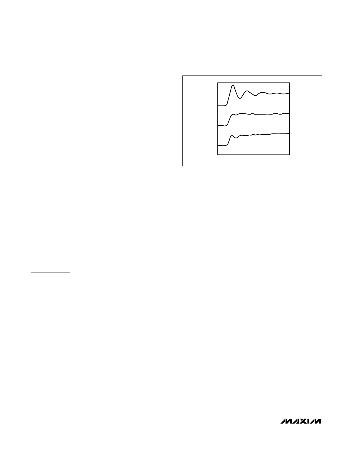
until the desired transmitter eye is obtained (Figure 13).
Quick Shutdown
To reduce laser shutdown time, a FET device can be
attached to SHDNDRV as shown in Figure 10. This provides a typical laser power shutdown time of less than
10µs.
Applications Information
Laser Safety and IEC 825
The International Electrotechnical Commission (IEC)
determines standards for hazardous light emissions
from fiber optic transmitters. IEC 825 defines the maximum light output for various hazard levels. The MAX3286/
MAX3296 series provides features that facilitate compliance with IEC 825.
A common safety requirement is single-point fault tolerance, whereby one unplanned short, open, or resistive
connection does not cause excess light output. When
these laser drivers are used, as shown in the Typical
Application Circuits, the circuits respond to faults as
listed in Table 5.
Using these laser drivers alone does not ensure that a
transmitter design is compliant with IEC 825. The entire
transmitter circuit and component selections must be
considered. Customers must determine the level of fault
tolerance required by their applications, recognizing that
Maxim products are not designed or authorized for use
as components in systems intended for surgical implant
into the body, for applications intended to support or sustain life, or for any other application where the failure of
a Maxim product could create a situation where personal injury or death may occur.
Layout Considerations
The MAX3286/MAX3296 series comprises high-frequency products. Their performance depends largely
upon the circuit board layout.
Use a multilayer circuit board with a dedicated ground
plane. Use short laser package leads placed close to
the modulator outputs. Power supplies must be capacitively bypassed to the ground plane with surface-mount
capacitors placed near the power-supply pins.
The dominant pole of the APC circuit is normally located at BIASDRV. To prevent a second pole in the APC
(which can lead to oscillations), ensure that parasitic
capacitance at MD is minimized.
Common Questions
Laser output is ringing or contains overshoot. This often is
caused by inductive laser packaging. Try reducing the
length of the laser leads. Modify the compensation components to reduce the driver’s output edge speed (see
Design Procedure). Extreme ringing can be caused by
low voltage at the OUT± pins. This might indicate that
pullup beads or a lower modulation current are needed.
Low-frequency oscillation on the laser output. This is
more prevalent at low temperatures. The APC might be
oscillating. Try increasing the value of C
BIASDRV
or
increasing the value of R
DEG
. Ensure that the parasitic
capacitance at the MD node is kept very small (<10pF).
The APC is not needed. Connect FLTDLY to ground to
disable fault detection. Connect MD to REF and MON to
V
CC
. BIASDRV and SHDNDRV can be left open.
TIME
UNCOMPENSATED
CORRECTLY COMPENSATED
OVERCOMPENSATED
POWER
Figure 13. Laser Compensation
Page 17
MAX3286–MAX3289/MAX3296–MAX3299
3.0V to 5.5V, 1.25Gbps/2.5Gbps
LAN Laser Drivers
______________________________________________________________________________________ 17
PIN NAME
CIRCUIT RESPONSE TO OVERVOLTAGE OR
SHORT TO V
CC
CIRCUIT RESPONSE TO UNDERVOLTAGE OR
SHORT TO GROUND
EN Normal condition for circuit operation Fault state* occurs
Does not affect laser powerFAULT Does not affect laser power
Does not affect laser powerPOR Does not affect laser power
Normal condition for circuit operation
EN
Fault state* occurs
Fault state* occursPORDLY Does not affect laser power
Fault state* occurs if VCCis less than +4.5VLV Does not affect laser power
If POL is a TTL LOW, a fault state* occurs; otherwise, the circuit is in normal operation
POL
If POL is a TTL HIGH, a fault state* occurs; otherwise, the circuit is in normal operation
MON
(also MAX3288/
MAX3298)
In common cathode without photodiode configuration, a fault state* occurs; otherwise, does not affect
laser power
Fault state* occurs
If POL is a TTL LOW, a fault state* occurs; otherwise, the circuit is in normal operation
POL
If POL is a TTL HIGH, a fault state* occurs; otherwise, the circuit is in normal operation
Does not affect laser power
SHDNDRV
(also MAX3287/
MAX3297/MAX3289/
MAX3299
Does not affect laser power. If optional FET is used,
the laser output is shut off.
FLTDLY
Any fault that occurs cannot be reset. Does not
affect laser power.
Does not affect laser power
Does not affect laser powerIN+, IN- Does not affect laser power
In common-cathode configurations, a fault state*
occurs; otherwise, does not affect laser power
REF Fault state* occurs
Fault state* occursMD Fault state* occurs
OUT+, OUT- Does not affect laser power Does not affect laser power
Fault state* occursMODSET Does not affect laser power
In common-anode configurations, the laser bias
current is shut off. In common cathode, high laser
power triggers a fault state.* Shutdown occurs if a
shutdown FET (M1) is used (Figures 9, 10).
BIASDRV
In common-cathode configurations, the laser bias
current is shut off. In common anode, high laser
power triggers a fault state.* Shutdown occurs if a
shutdown FET (M1) is used. If shutdown FET is not
used, other means must be used to prevent high
laser power.
Fault state* occursTC Does not affect laser power
Table 5. Circuit Response to Various Single-Point Faults
*A fault state asserts the FAULT pins, disables the modulator outputs, disables the bias output, and asserts the SHDNDRV pin.
FAULT
Does not affect laser power Does not affect laser power
Page 18

MAX3286–MAX3289/MAX3296–MAX3299
3.0V to 5.5V, 1.25Gbps/2.5Gbps
LAN Laser Drivers
18 ______________________________________________________________________________________
The modulator is not needed. Leave TC and MODSET
open. Connect IN+ to VCC, IN- to REF, and leave OUT+
and OUT– open.
Wirebonding Die
The MAX3286/MAX3296 series uses bondpads with gold
metalization. Make connections to the die with gold wire
only, using ball-bonding techniques. Wedge bonding is
not recommended. Bondpad size is 4 mil square. Die
thickness is typically 15 mils (0.38mm).
Interface Models
Figures 14–18 show typical input/output models for the
MAX3286/MAX3296 series of laser drivers. If dice are
used, replace the package parasitic elements with
bondwire parasitic elements.
4kΩ
2.5kΩ
V
CC
FAULT, FAULT, POR
MAX3286
MAX3296
Figure 14. Logic Outputs
10kΩ
550Ω
60Ω
V
CC
SHDNDRV
MAX3286
MAX3296
Figure 15. SHDNDRV Output
PACKAGE
V
CC
V
CC
1.5nH
OUT-
0.2pF
1.5nH
0.2pF
OUT+
50Ω
50Ω
PACKAGE
1pF 1pF
Figure 16. Modulator Outputs
Page 19
MAX3286–MAX3289/MAX3296–MAX3299
3.0V to 5.5V, 1.25Gbps/2.5Gbps
LAN Laser Drivers
______________________________________________________________________________________ 19
40Ω
40Ω
V
CC
BIASDRV
MAX3286
MAX3296
Figure 18. BIASDRV Output
Q1
Q2
1.5nH
1.5nH
INPUT COMMON-MODE VOLTAGE ≈ V
CC
- 0.3V
R
IN
Q1, Q2 > 100kΩ
PACKAGE
0.2pF
0.2pF
V
CC
V
CC
V
CC
400Ω
400Ω
1pF
1pF
IN+
IN-
MAX3286
MAX3296
Figure 17. Data Inputs
Page 20
MAX3286–MAX3289/MAX3296–MAX3299
3.0V to 5.5V, 1.25Gbps/2.5Gbps
LAN Laser Drivers
20 ______________________________________________________________________________________
*Dice are designed to operate from TJ= 0°C to +110°C, but are
tested and guaranteed only at TA= +25°C.
**Exposed pad.
***Package Code: G2855-1
****Package Code: T2855-7
+Denotes Lead-Free Package.
Selector Guide
Ordering Information (continued)
PART TEMP RANGE PIN-PACKAGE
MAX3286C/D 0°C to +70°C Dice*
MAX3287CUE 0°C to +70°C 16 TSSOP-EP**
MAX3288CUE 0°C to +70°C 16 TSSOP-EP**
MAX3289CUE 0°C to +70°C 16 TSSOP-EP**
MAX3296CTI+ 0°C to +70°C
28 Thin QFN
(5mm x 5mm)****
MAX3296CGI 0°C to +70°C
28 QFN
(5mm x 5mm)***
MAX3296CHJ 0°C to +70°C
32 TQFP
(5mm x 5mm)
MAX3296C/D 0°C to +70°C Dice*
MAX3297CUE 0°C to +70°C 16 TSSOP-EP**
MAX3298CUE 0°C to +70°C 16 TSSOP-EP**
MAX3299CUE 0°C to +70°C 16 TSSOP-EP**
DATA RATE/DEVICE LASER CONFIGURATION
COMMON
ANODE
1.25Gbps 2.5Gbps
MAX3286 MAX3296 ✓✓✓
MAX3287 MAX3297 ✓ 16 TSSOP-EP
MAX3288 MAX3298 ✓ 16 TSSOP-EP
MAX3289 MAX3299 ✓ 16 TSSOP-EP
WITH
PHOTODIODE
Longwave
COMMON
CATHODE
WITH
PHOTODIODE
Shortwave or
VCSEL
COMMON
CATHODE
WITH
PHOTODIODE
VCSEL
32 TQFP/28 QFN/
28 Thin QFN/Dice
PACKAGE
Page 21
MAX3286–MAX3289/MAX3296–MAX3299
3.0V to 5.5V, 1.25Gbps/2.5Gbps
LAN Laser Drivers
______________________________________________________________________________________ 21
16
15
14
13
12
11
10
9
1
2
3
4
5
6
7
8
GND TC
MODSET
V
CC
OUT-
OUT+
V
CC
BIASDRV
MON
MAX3288
MAX3298
TSSOP-EP*
FLTDLY
V
CC
GND
IN+
IN-
REF
MD
16
15
14
13
12
11
10
9
1
2
3
4
5
6
7
8
GND TC
MODSET
V
CC
OUT-
OUT+
V
CC
BIASDRV
SHDNDRV
MAX3287
MAX3289
MAX3297
MAX3299
TSSOP-EP*
FLTDLY
V
CC
GND
IN+
IN-
REF
MD
*EXPOSED PAD IS CONNECTED TO GND.
MAX3286
MAX3296
TQFP
32 28
293031
25
26
27
MODSET
GND
VCCOUT-TCOUT+
VCCV
CC
10
13
15
14
1611 12
9
FLTDLY
V
CC
LV
IN-
IN+
REF
GND
N.C.
17
18
19
20
21
22
23
SHDNDRV
24 BIASDRV
GND
MON
MD
N.C.
POL
POL
2
3
4
5
6
7
8PORDLY
EN
GND
POR
FAULT
N.C.
1FAULT
EN
28
27
26
25
242322
TC
MODSET
V
CC
OUT-
OUT+
VCCV
CC
8
9
10
11
121314
FLTDLY
LV
V
CC
IN+
IN-
GND
REF
15
16
17
18
19
20
21
POL
POL
MD
MON
GND
SHDNDRV
BIASDRV
7
6
5
4
3
2
1
PORDLY
EN
EN
GND
POR
FAULT
FAULT
MAX3286
MAX3296
QFN*
TOP VIEW
Pin Configurations (continued)
Page 22
MAX3286–MAX3289/MAX3296–MAX3299
3.0V to 5.5V, 1.25Gbps/2.5Gbps
LAN Laser Drivers
22 ______________________________________________________________________________________
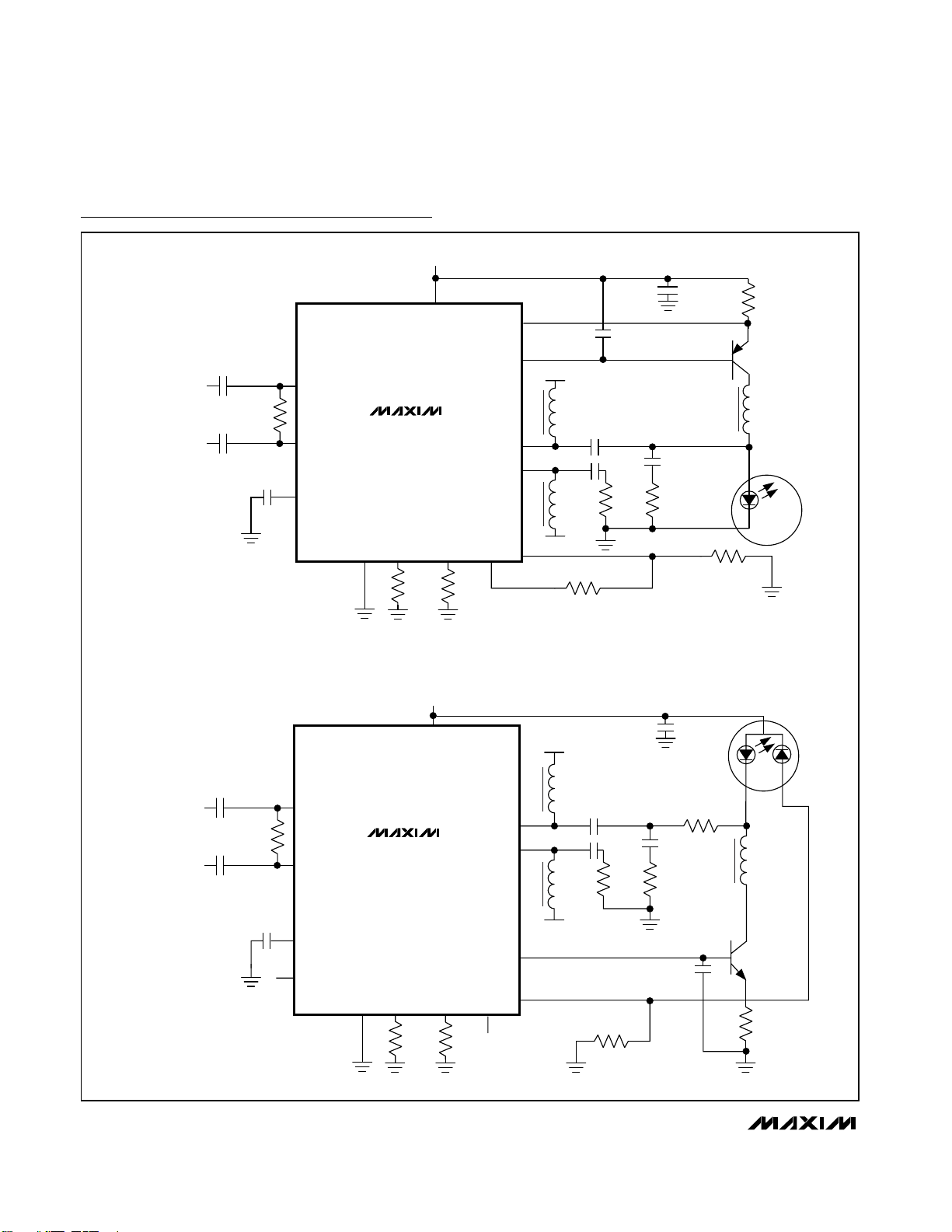
Typical Application Circuits
POL
IN-
POL
FLTDLY
FAULT
FAULT
POR
EN
EN
IN+
OUT-
OUT+
MD
REF
MON
MODSET
TC
GND
SHDNDRV
BIASDRV
PORDLY
V
CC
115Ω
+3.0V TO +5.5V
FERRITE
BEAD
PMOSFET
(OPTIONAL)
PNP
TRANSISTOR
25Ω
0.01µF
R
TC
R
MOD
R
SET
0.01µF
0.01µF
C
COMP
DATA
INPUT
C
BIASDRV
0.1µF
LV
V
CC
R
COMP
0.01µF
V
CC
MAX3286
MAX3296
0.01µF
MAX3286/MAX3296
COMMON-CATHODE VCSEL
WITH PHOTODIODE
0.01µF
0.01µF
0.01µF
R
1kΩ
0.01µF
SET
C
0.1µF
25Ω
BIASDRV
MAX3286/MAX3296
COMMON-CATHODE VCSEL
WITHOUT PHOTODIODE
0.01µF
DATA
INPUT
0.01µF
115Ω
0.01µF
0.01µF
FLTDLY
PORDLY
IN+
INSHDNDRV
POR
FAULT
LV
FAULT
EN
POL
GND
POL
+3.0V TO +5.5V
EN
MAX3286
MAX3296
TC
R
TC
V
CC
MODSET
MON
BIASDRV
V
CC
OUT+
OUT-
V
CC
REF
MD
R
MOD
C
COMP
R
COMP
0.01µF
R
5kΩ
MD
R
MON
PNP
TRANSISTOR
FERRITE
BEAD
Page 23
MAX3286–MAX3289/MAX3296–MAX3299
3.0V to 5.5V, 1.25Gbps/2.5Gbps
LAN Laser Drivers
______________________________________________________________________________________ 23
Typical Application Circuits (continued)
POL
IN-
POL
FLTDLY
FAULT
FAULT
POR
EN
EN
IN+
OUT-
OUT+
MD
REF
MON
MODSET
TC
GND
SHDNDRV
BIASDRV
PORDLY
V
CC
115Ω
+3.0V TO +5.5V
FERRITE
BEAD
NPN
TRANSISTOR
25Ω
0.01µF
R
TC
R
MOD
R
SET
R
DEG
0.01µF
0.01µF
C
COMP
DATA
INPUT
LV
V
CC
R
COMP
0.01µF
V
CC
MAX3286
MAX3296
0.01µF
C
BIASDRV
0.1µF
MAX3286/MAX3296
COMMON-ANODE LASER
WITH PHOTODIODE
0.01µF
0.01µF
18Ω
COMMON-CATHODE VCSEL
MAX3287/MAX3297
WITH PHOTODIODE
0.01µF
0.01µF
DATA
INPUT
115Ω
0.01µF
IN+
IN-
FLTDLY
MAX3287
MAX3297
+3.0V TO +5.5V
V
CC
BIASDRV
OUT+
OUT-
V
CC
0.01µF
0.01µF
C
BIASDRV
0.1µF
25Ω
0.01µF
C
COMP
R
COMP
R
DEG
PNP
TRANSISTOR
FERRITE
BEAD
SHDNDRV
GND
MODSET
TC
R
TC
REF
R
MOD
MD
V
CC
R
SET
Page 24
MAX3286–MAX3289/MAX3296–MAX3299
3.0V to 5.5V, 1.25Gbps/2.5Gbps
LAN Laser Drivers
24 ______________________________________________________________________________________
Typical Application Circuits (continued)
IN-
FLTDLY
IN+
OUT-
OUT+
MD
REF
MODSET
TC
GND
BIASDRV
V
CC
115Ω
+3.0V TO +5.5V
FERRITE
BEAD
PNP
TRANSISTOR
25Ω
0.01µF
R
TC
R
MOD
R
SET
1kΩ
0.01µF
C
COMP
DATA
INPUT
C
BIASDRV
0.1µF
R
COMP
0.01µF
MAX3288
MAX3298
MON
R
MON
R
MD
5kΩ
0.01µF
MAX3288/MAX3298
COMMON-CATHODE VCSEL
WITHOUT PHOTODIODE
V
CC
V
CC
0.01µF
0.01µF
MAX3289/MAX3299
COMMON-ANODE LASER
+3.0V to +5.5V
V
CC
V
CC
WITH PHOTODIODE
0.01µF
DATA
115Ω
INPUT
0.01µF
IN+
0.01µF
0.01µF
25Ω
C
R
COMP
COMP
OUT-
MAX3289
IN-
MAX3299
OUT+
0.01µF
18Ω
FERRITE
BEAD
0.01µF
FLTDLY
SHDNDRV
GND
BIASDRV
MODSET
TC
R
TC
MD
REF
R
MOD
V
CC
C
BIASDRV
0.1µF
R
SET
NPN
TRANSISTOR
R
DEG
Page 25
MAX3286–MAX3289/MAX3296–MAX3299
3.0V to 5.5V, 1.25Gbps/2.5Gbps
LAN Laser Drivers
______________________________________________________________________________________ 25
TC
V
CC
OUT-
OUT+
V
CC
V
CC
LV
V
CC
IN+
IN-
GND
REF
0.053"
(1.346mm)
MON
POL
GND
MD
POL
GNDENPOR
EN
N.C.
0.072"
(1.829mm)
SHDNDRV
BIASDRV
MODSET
FAULT
FAULT
PORDLY
FLTDLY
HF34Z-1Z
TC
V
CC
V
CC
V
CC
LV
V
CC
IN+
IN-
GND
REF
MON
POL
GND
MD
POL
GNDENPOR
EN
N.C.
0.072"
(1.829mm)
SHDNDRV
BIASDRV
MODSET
FAULT
FAULT
PORDLY
FLTDLY
HF34Z
0.053"
(1.346mm)
OUT-
OUT+
Chip Topographies
TRANSISTOR COUNT: 1154
SUBSTRATE CONNECTED TO GND
TRANSISTOR COUNT: 1154
SUBSTRATE CONNECTED TO GND
MAX3286 MAX3296
Page 26
MAX3286–MAX3289/MAX3296–MAX3299
3.0V to 5.5V, 1.25Gbps/2.5Gbps
LAN Laser Drivers
26 ______________________________________________________________________________________
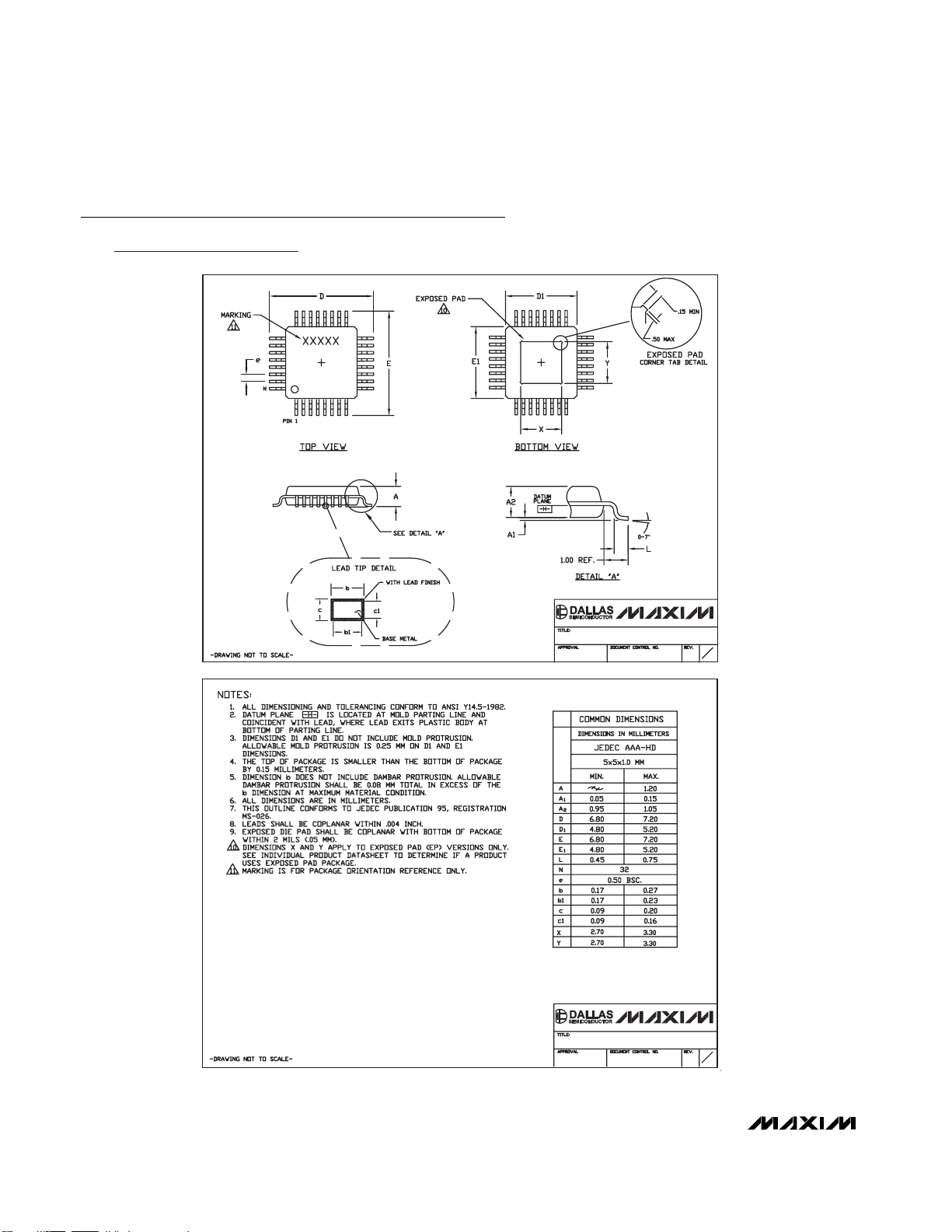
32L,TQFP.EPS
F
1
2
21-0079
PACKAGE OUTLINE,
32L TQFP, 5x5x1.0mm, EP OPTION
F
2
2
21-0079
PACKAGE OUTLINE,
32L TQFP, 5x5x1.0mm, EP OPTION
Package Information (continued)
(The package drawing(s) in this data sheet may not reflect the most current specifications. For the latest package outline information,
go to www.maxim-ic.com/packages
.)
Page 27

MAX3286–MAX3289/MAX3296–MAX3299
3.0V to 5.5V, 1.25Gbps/2.5Gbps
LAN Laser Drivers
______________________________________________________________________________________ 27
32L QFN.EPS
Package Information (continued)
(The package drawing(s) in this data sheet may not reflect the most current specifications. For the latest package outline information,
go to www.maxim-ic.com/packages
.)
Page 28
MAX3286–MAX3289/MAX3296–MAX3299
3.0V to 5.5V, 1.25Gbps/2.5Gbps
LAN Laser Drivers
Maxim makes no warranty, representation or guarantee regarding the suitability of its products for any particular purpose, nor does Maxim assume any liability arising out of the application or use of any product or circuit and specifically disclaims any and all liability, including without limitation consequential or
incidental damages. “Typical” parameters can and do vary in different applications. All operating parameters, including “typicals” must be validated for
each customer application by customer’s technical experts. Maxim products are not designed, intended or authorized for use as components in systems
intended for surgical implant into the body, or other applications intended to support or sustain life, or for any other application in which the failure of the
Maxim product could create a situation where personal injury or death may occur.
Maxim Integrated Products, 120 San Gabriel Drive, Sunnyvale, CA 94086 408-737-7600 ____________________ 28
© 2004 Maxim Integrated Products Printed USA is a registered trademark of Maxim Integrated Products.
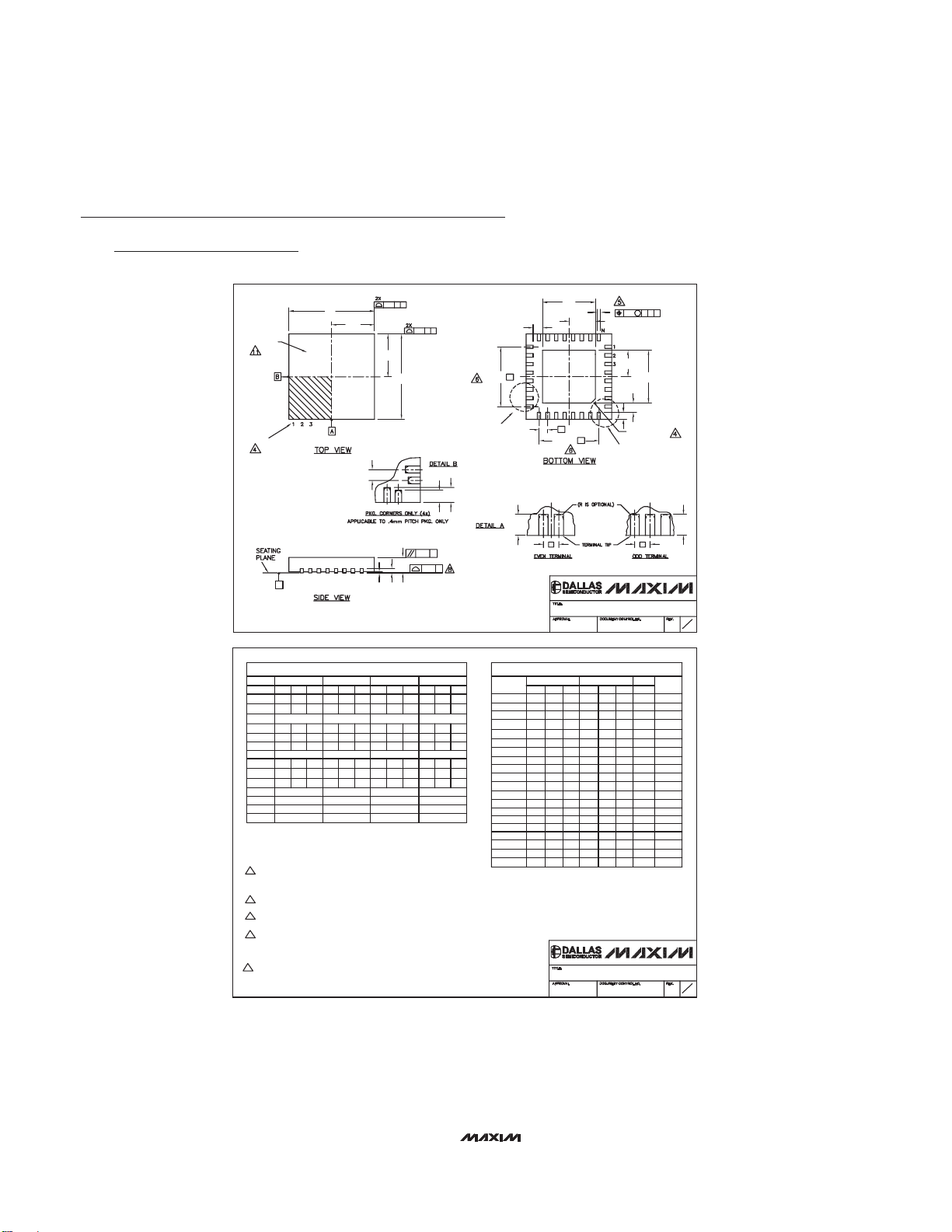
QFN THIN.EPS
D2
(ND-1) X e
e
D
C
PIN # 1
I.D.
(NE-1) X e
E/2
E
0.08 C
0.10 C
A
A1
A3
DETAIL A
0.15
C B
0.15 C A
E2/2
E2
0.10 M C A B
PIN # 1 I.D.
b
0.35x45∞
L
D/2
D2/2
L
C
L
C
e e
L
CC
L
k
k
LL
DETAIL B
L
L1
e
XXXXX
MARKING
F
1
2
21-0140
PACKAGE OUTLINE,
16, 20, 28, 32L THIN QFN, 5x5x0.8mm
-DRAWING NOT TO SCALE-
COMMON DIMENSIONS
3.353.15
T2855-1 3.25 3.353.15 3.25
MAX.
3.20
EXPOSED PAD VARIATIONS
3.00T2055-2 3.10
D2
NOM.MIN.
3.203.00 3.10
MIN.E2NOM. MAX.
NE
ND
PKG.
CODES
1. DIMENSIONING & TOLERANCING CONFORM TO ASME Y14.5M-1994.
2. ALL DIMENSIONS ARE IN MILLIMETERS. ANGLES ARE IN DEGREES.
3. N IS THE TOTAL NUMBER OF TERMINALS.
4. THE TERMINAL #1 IDENTIFIER AND TERMINAL NUMBERING CONVENTION SHALL
CONFORM TO JESD 95-1 SPP-012. DETAILS OF TERMINAL #1 IDENTIFIER ARE
OPTIONAL, BUT MUST BE LOCATED WITHIN THE ZONE INDICATED. THE TERMINAL #1
IDENTIFIER MAY BE EITHER A MOLD OR MARKED FEATURE.
5. DIMENSION b APPLIES TO METALLIZED TERMINAL AND IS MEASURED BETWEEN 0.25 mm AND 0.30 mm
FROM TERMINAL TIP.
6. ND AND NE REFER TO THE NUMBER OF TERMINALS ON EACH D AND E SIDE RESPECTIVELY.
7. DEPOPULATION IS POSSIBLE IN A SYMMETRICAL FASHION.
8. COPLANARITY APPLIES TO THE EXPOSED HEAT SINK SLUG AS WELL AS THE TERMINALS.
9. DRAWING CONFORMS TO JEDEC MO220, EXCEPT EXPOSED PAD DIMENSION FOR T2855-1,
T2855-3 AND T2855-6.
NOTES:
SYMBOL
PKG.
N
L1
e
E
D
b
A3
A
A1
k
10. WARPAGE SHALL NOT EXCEED 0.10 mm.
JEDEC
T1655-1
3.203.00 3.10 3.00 3.10 3.20
0.70 0.800.75
4.90
4.90
0.25
0.250--
4
WHHB
4
16
0.350.30
5.10
5.105.00
0.80 BSC.
5.00
0.05
0.20 REF.
0.02
MIN. MAX.NOM.
16L 5x5
3.10
T3255-2
3.00
3.20
3.00 3.10 3.20
2.70
T2855-2 2.60 2.602.80 2.70 2.80
L
0.30 0.500.40
---
---
WHHC
20
5
5
5.00
5.00
0.30
0.55
0.65 BSC.
0.45
0.25
4.90
4.90
0.25
0.65
--
5.10
5.10
0.35
20L 5x5
0.20 REF.
0.75
0.02
NOM.
0
0.70
MIN.
0.05
0.80
MAX.
---
WHHD-1
28
7
7
5.00
5.00
0.25
0.55
0.50 BSC.
0.45
0.25
4.90
4.90
0.20
0.65
--
5.10
5.10
0.30
28L 5x5
0.20 REF.
0.75
0.02
NOM.
0
0.70
MIN.
0.05
0.80
MAX.
---
WHHD-2
32
8
8
5.00
5.00
0.40
0.50 BSC.
0.30
0.25
4.90
4.90
0.50
--
5.10
5.10
32L 5x5
0.20 REF.
0.75
0.02
NOM.
0
0.70
MIN.
0.05
0.80
MAX.
0.20 0.25 0.30
DOWN
BONDS
ALLOWED
NO
YES3.103.00 3.203.103.00 3.20T2055-3
3.103.00 3.203.103.00 3.20T2055-4
T2855-3 3.15 3.25 3.35 3.15 3.25 3.35
T2855-6 3.15 3.25 3.35 3.15 3.25 3.35
T2855-4 2.60 2.70 2.80 2.60 2.70 2.80
T2855-5 2.60 2.70 2.80 2.60 2.70 2.80
T2855-7 2.60 2.70
2.80
2.60 2.70 2.80
3.203.00 3.10T3255-3 3.203.00 3.10
3.203.00 3.10T3255-4 3.203.00 3.10
NO
NO
NO
NO
NO
NO
NO
NO
YES
YES
YES
YES
3.203.00T1655-2 3.10 3.00 3.10 3.20 YES
NO3.203.103.003.10T1655N-1 3.00 3.20
3.353.15T2055-5 3.25 3.15 3.25 3.35
Y
3.35
3.15T2855N-1 3.25 3.15 3.25 3.35
N
3.35
3.15T2855-8 3.25 3.15 3.25 3.35
Y
3.203.10T3255N-1 3.00
NO
3.203.103.00
L
0.40
0.40
**
**
**
**
**
**
**
**
**
**
**
**
**
**
**
**
**
**
**
SEE COMMON DIMENSIONS TABLE
±0.15
11. MARKING IS FOR PACKAGE ORIENTATION REFERENCE ONLY.
F
2
2
21-0140
PACKAGE OUTLINE,
16, 20, 28, 32L THIN QFN, 5x5x0.8mm
-DRAWING NOT TO SCALE-
12. NUMBER OF LEADS SHOWN ARE FOR REFERENCE ONLY.
Package Information (continued)
(The package drawing(s) in this data sheet may not reflect the most current specifications. For the latest package outline information,
go to www.maxim-ic.com/packages
.)
 Loading...