

Page 1

现货库存、技术资料、百科信息、热点资讯,精彩尽在鼎好!
MAX3283EAUT
Rev. A
RELIABILITY REPORT
FOR
MAX3283EAUT
PLASTIC ENCAPSULATED DEVICES
February 14, 2003
MAXIM INTEGRATED PRODUCTS
120 SAN GABRIEL DR.
SUNNYVALE, CA 94086
Written by Reviewed by
Jim Pedicord Bryan J. Preeshl
Quality Assurance Quality Assurance
Reliability Lab Manager Executive Director
Page 2

Conclusion
The MAX3283E successfully meets the quality and reliability standards required of all Maxim products. In
addition, Maxim’s continuous reliability monitoring program ensures that all outgoing product will continue to meet Maxim’s
quality and reliability standards.
Table of Contents
I. ........Device Description V. ........Quality Assurance Information
II. ........Manufacturing Information VI. .......Reliability Evaluation
III. .......Packaging Information
IV. .......Die Information ......Attachments
I. Device Description
A. General
The MAX3283E is a single receiver designed for RS -485 and RS-422 communication. This devices guarantee data
rates up to 52Mbps, even with a 3V power supply. Excellent propagation delay (15ns max) and package-to-package
skew time (8ns max) make this device ideal for multidrop clock distribution applications.
The MAX3283E has true fail-safe circuitry, which guarantees a logic-high receiver output when the receiver inputs are
opened or shorted. The receiver output will be a logic high if all transmitters on a terminated bus are disabled (high
impedance). This device features 1/4-unit-load receiver input impedance, allowing up to 128 receivers on the same
bus.
The MAX3283E single receivers have a receiver enable (EN or EN-bar) function and are offered in a 6-pin SOT23
package.
B. Absolute Maximum Ratings
Item Rating
(All Voltages Referenced to GND)
Supply Voltage (VCC) -0.3V to +6V
Control Input Voltage (EN, EN ) -0.3V to +6V
VL Input Voltage -0.3V to +6V
Receiver Input Voltage (A, B) -7.5V to +12.5V
Receiver Output Voltage (RO) -0.3V to (VCC + 0.3V)
Receiver Output Short -Circuit Current Continuous
Operating Temperature Range -40°C to +125°C
Storage Temperature Range -65°C to +150°C
Junction Temperature +150°C
Lead Temperature (soldering, 10s) +300°C
Continuous Power Dissipation (TA = +70°C)
6-Pin SOT23 696mW
Derates above +70°C
6-Pin SOT23 8.7mW/°C
Page 3

II. Manufacturing Information
A. Description/Function: ±15kV ESD-Protected 52Mbps, 3V to 5.5V, RS-485/RS-422 True Fail-Safe Receivers
B. Process: S8 - Standard 8 micron silicon gate CMOS
C. Number of Device Transistors: 233
D. Fabrication Location: California, USA
E. Assembly Location: Malaysia or Thailand
F. Date of Initial Production: January, 2002
III. Packaging Information
A. Package Type: 6-Lead SOT23
B. Lead Frame: Copper
C. Lead Finish: Solder Plate
D. Die Attach: Silver-Filled Epoxy
E. Bondwire: Gold (1.0 mil dia.)
F. Mold Material: Epoxy with silica filler
G. Assembly Diagram: Buildsheet # 05-9000-0327
H. Flammability Rating: Class UL94-V0
I. Classifi cation of Moisture Sensitivity
per JEDEC standard JESD22-A112: Level 1
IV. Die Information
A. Dimensions: 43 X 35 mils
B. Passivation: Si3N4/SiO2 (Silicon nitride/ Silicon dioxide)
C. Interconnect: TiW/ AlCu/ TiWN
D. Backside Metallization: None
E. Minimum Metal Width: .8 microns (as drawn)
F. Minimum Metal Spacing: .8 microns (as drawn)
G. Bondpad Dimensions: 2.7 mil. Sq.
H. Isolation Dielectric: SiO
2
I. Die Separation Method: Wafer Saw
Page 4

V. Quality Assurance Information
A. Quality Assurance Contacts: Jim Pedicord (Reliability Lab Manager)
Bryan Preeshl ( Executive Director of QA)
Kenneth Huening (Vice President)
B. Outgoing Inspection Level: 0.1% for all electrical parameters guaranteed by the Datasheet.
0.1% For all Visual Defects.
C. Observed Outgoing Defect Rate: < 50 ppm
D. Sampling Plan: Mil-Std-105D
VI. Reliability Evaluation
A. Accelerated Life Test
The results of the 135°C biased (static) life test are shown in Table 1. Using these results, the Failure
Rate (λ ) is calculated as follows:
λ = 1 = 1.83 (Chi square value for MTTF upper limit)
MTTF 192 x 4389 x 240 x 2
Temperature Acceleration factor assuming an activation energy of 0.8eV
λ = 4.52 x 10
-9
λ = 4.52 F.I.T. (60% confidence level @ 25°C)
This low failure rate represents data collected from Maxim’s reliability qualification and monitor programs.
Maxim also performs weekly Burn-In on samples from production to assure reliability of its processes. The
reliability required for lots which receive a burn-in qualification is 59 F.I.T. at a 60% confidence level, which equates
to 3 failures in an 80 piece sample. Maxim performs failure analysis on rejects from lots exceeding this level. The
Burn-In Schematic (Spec.# 06-5867) shows the static circuit used for this test. Maxim also performs 1000 hour life
test monitors quarterly for each process. This data is published in the Product Reliability Report (RR-1M) located
on the Maxim website at http://www.maxim-ic.com
.
B. Moisture Resistance Tests
Maxim evaluates pressure pot stress from every assembly process during qualification of each new design.
Pressure Pot testing must pass a 20% LTPD for acceptance. Additionally, industry standard 85°C/85%RH or
HAST tests are performed quarterly per device/package family.
C. E.S.D. and Latch-Up Testing
The RT33-3 die type has been found to have all pins able to withstand a transient pulse of ±1000V, per Mil-
Std-883 Method 3015 (reference attached ESD Test Circuit). Additionally, the MAX3283E has achieved ±15kV
ESD protection using both methods 3015 and IEC 801-2 (air-gap discharge) on the I/O pins.
Latch-Up testing has shown that this device withstands a current of ±250mA and/or ±20V.
Page 5

Table 1
Reliability Evaluation Test Results
MAX3283EAUT
TEST ITEM TEST CONDITION FAILURE SAMPLE NUMBER OF
IDENTIFICATION SIZE FAILURES
Static Life Test (Note 1)
Ta = 135°C DC Parameters 240 0
Biased & functionality
Time = 192 hrs.
Moisture Testing (Note 2)
Pressure Pot Ta = 121°C DC Parameters 77 0
P = 15 psi. & functionality
RH= 100%
Time = 168hrs.
85/85 Ta = 85°C DC Parameters 77 0
RH = 85% & functionality
Biased
Time = 1000hrs.
Mechanical Stress (Note 2)
Temperature -65°C/150°C DC Parameters 77 0
Cycle 1000 Cycles
Method 1010
Note 1: Life Test Data may represent plastic D.I.P. qualification lots.
Note 2: Generic process/package data
Page 6
Attachment #1
Mil Std 883D
TERMINAL D
TABLE II. Pin combination to be tested. 1/ 2/
1.
2.
(Each pin individually
connected to terminal A
with the other floating)
All input and output pins All other input-output pins
Terminal A
All pins except V
PS1
3/
1/ Table II is restated in narrative form in 3.4 below.
2/ No connects are not to be tested.
3/ Repeat pin combination I for each named Power supply and for ground
(e.g., where V
is VDD, VCC, VSS, VBB, GND, +VS, -VS, V
PS1
3.4 Pin combinations to be tested.
a. Each pin individually connected to terminal A with respect to the device ground pin(s) connected
to terminal B. All pins except the one being tested and the ground pin(s) shall be open.
b. Each pin individually connected to terminal A with respect to each different set of a combination
of all named power supply pins (e.g., V
SS1
terminal B. All pins except the one being tested and the power supply pin or set of pins shall be
open.
c. Each input and each output individually connected to terminal A with respect to a combination of
all the other input and output pins connected to terminal B. All pins except the input or output pin
being tested and the combination of all the other input and output pins shall be open.
Terminal B
(The common combination
of all like-named pins
connected to terminal B)
All V
PS1
pins
REF
, or V
SS2
or V
SS3
or V
CC1
, etc).
, or V
) connected to
CC2
Method 3015.7
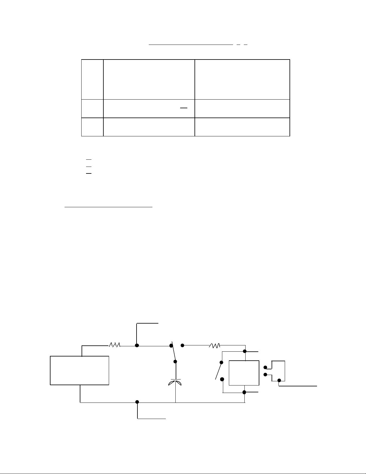
Notice 8
REGULATED
HIGH VOLTAGE
SUPPLY
R1
TERMINAL C
S1
C1
S2
R2
DUT
SOCKET
TERMINAL A
SHORT
TERMINAL B
R = 1.5kΩΩ
C = 100pf
CURRENT
PROBE
(NOTE 6)
Page 7

Page 8

ONCE PER SOCKET
ONCE PER BOARD
+5V
1
2
3
DEVICES: MAX 3281
MAX. EXPECTED CURRENT = 12 mA
6 PIN SOT
6
10 K
5
4
DRAWN BY: TEK TAN
NOTES:
DOCUMENT I.D. 06-5876 REVISION A
MAXIM TITLE: BI Circuit (MAX3281) PAGE 2 OF 3
 Loading...