

Page 1
General Description
The MAX3280E/MAX3281E/MAX3283E/MAX3284E are
single receivers designed for RS-485 and RS-422 communication. These devices guarantee data rates up to
52Mbps, even with a 3V power supply. Excellent propagation delay (15ns max) and package-to-package
skew time (8ns max) make these devices ideal for multidrop clock distribution applications.
The MAX3280E/MAX3281E/MAX3283E/MAX3284E
have true fail-safe circuitry, which guarantees a logichigh receiver output when the receiver inputs are
opened or shorted. The receiver output will be a logic
high if all transmitters on a terminated bus are disabled
(high impedance). These devices feature 1/4-unit-load
receiver input impedance, allowing up to 128 receivers
on the same bus.
The MAX3280E is a single receiver available in a 5-pin
SOT23 package. The MAX3281E/MAX3283E single
receivers have a receiver enable (EN or EN) function
and are offered in a 6-pin SOT23 package. The
MAX3284E features a voltage logic pin that allows compatibility with low-voltage logic levels, as in digital
FPGAs/ASICs. On the MAX3284E, the voltage threshold
for a logic high is user-defined by setting VLin the
range from 1.65V to V
CC
. The MAX3284E is also
offered in a 6-pin SOT23 package.
Applications
Clock Distribution
Telecom Racks
Base Stations
Industrial Control
Local Area Networks
Features
♦ ESD Protection:
±15kV Human Body Model
±6kV IEC 1000-4-2, Contact Discharge
±12kV IEC 1000-4-2, Air-Gap Discharge
♦ Guaranteed 52Mbps Data Rate
♦ Guaranteed 15ns Receiver Propagation Delay
♦ Guaranteed 2ns Receiver Skew
♦ Guaranteed 8ns Package-to-Package Skew Time
♦ V
L
Pin for Connection to FPGAs/ASICs
♦ Allow Up to 128 Transceivers on the Bus
(1/4-unit-load)
♦ Tiny SOT23 Package
♦ True Fail-Safe Receiver
♦ -7V to +12V Common-Mode Range
♦ 3V to 5.5V Power-Supply Range
♦ Enable (High and Low) Pins for Redundant
Operation
♦ Three-State Output Stage (MAX3281E/MAX3283E)
♦ Thermal Protection Against Output Short Circuit
MAX3280E/MAX3281E/MAX3283E/MAX3284E
±15kV ESD-Protected 52Mbps, 3V to 5.5V, SOT23
RS-485/RS-422 True Fail-Safe Receivers
________________________________________________________________
Maxim Integrated Products
1
Ordering Information
19-2320; Rev 1; 3/11
For pricing, delivery, and ordering information, please contact Maxim Direct at 1-888-629-4642,
or visit Maxim’s website at www.maxim-ic.com.
Pin Configurations appear at end of data sheet.
Selector Guide
Note 1: MAX3284E data rate is dependent on VL.
+
Denotes a lead(Pb)-free/RoHS-compliant package.
T = Tape and reel.
PART TEMP RANGE
MAX3280E AUK+T -40°C to +125°C 5 SOT23-5 ADVM
MAX3281EAUT+T -40°C to +125°C 6 SOT23-6 ABAT
MAX3283EAUT+T -40°C to +125°C 6 SOT23-6 ABAU
MAX3284EAUT+T -40°C to +125°C 6 SOT23-6 ABAV
PINPACKAGE
TOP
MARK
PART V
MAX3280E — — 52Mbps 5-Pin SOT23
MAX3281E — Active High 52Mbps 6-Pin SOT23
MAX3283E — Active Low 52Mbps 6-Pin SOT23
MAX3284E ✔ —
L
ENABLE DATA RATE PACKAGE
52Mbps (Note 1)
6-Pin SOT23
Page 2
MAX3280E/MAX3281E/MAX3283E/MAX3284E
±15kV ESD-Protected 52Mbps, 3V to 5.5V, SOT23
RS-485/RS-422 True Fail-Safe Receivers
2 _______________________________________________________________________________________
ABSOLUTE MAXIMUM RATINGS
ELECTRICAL CHARACTERISTICS
(VCC= 3V to 5.5V, VL= VCC, TA= T
MIN
to T
MAX
, unless otherwise noted. Typical values are at VCC= 5V and TA= +25°C.) (Notes 2, 3)
Stresses beyond those listed under “Absolute Maximum Ratings” may cause permanent damage to the device. These are stress ratings only, and functional
operation of the device at these or any other conditions beyond those indicated in the operational sections of the specifications is not implied. Exposure to
absolute maximum rating conditions for extended periods may affect device reliability.
(All Voltages Referenced to GND)
Supply Voltage (V
CC
) ...............................................-0.3V to +6V
Control Input Voltage (EN, EN).................................-0.3V to +6V
V
L
Input Voltage .......................................................-0.3V to +6V
Receiver Input Voltage (A, B)..............................-7.5V to +12.5V
Receiver Output Voltage (RO)....................-0.3V to (V
CC
+ 0.3V)
Receiver Output Voltage
(RO) (MAX3284E) .....................................-0.3V to (VL+ 0.3V)
Receiver Output Short-Circuit Current .......................Continuous
Continuous Power Dissipation (T
A
= +70°C)
5-Pin SOT23 (derate 7.1mW/°C above +70°C)............571mW
6-Pin SOT23 (derate 8.7mW/°C above +70°C)............696mW
Operating Temperature Range
MAX328_EA__ ..............................................-40°C to +125°C
Storage Temperature Range .............................-65°C to +150°C
Junction Temperature......................................................+150°C
Lead Temperature (soldering, 10s) .................................+300°C
Soldering Temperature (reflow) .......................................+260°C
Supply Voltage VCC 3.0 5.5 V
Supply Current ICC No load 9 15 mA
VL Input Range VL MAX3284E 1.65 VCC V
VL Supply C urrent IL No load (MAX3284E) 10 μA
RECEIVER
Input Current (A and B) I
Receiver Differential Threshold
Voltage
Receiver Input Hysteresis VTH VA + VB = 0V 25 mV
Receiver Enable Input Low V
Receiver Enable Input High V
Receiver Enable Input Leakage I
Receiver Output High Voltage V
Receiver Output Low Voltage V
Three-State Output Current at
Receiver
Receiver Input Resistance RIN -7V VCM +12V (Note 5) 48 k
Receiver Output Short-Circuit
Current
ESD PROTECTION
ESD Protection (A, B)
PARAMETER S YMBOL CONDITIONS MIN TYP MAX UNITS
VCC = V
A, B
V
-7V VCM +12V (Note 4) -200 -125 -50 mV
TH
MAX3281E, MAX3283E onl y 0.4 V
ENIL
MAX3281E, MAX3283E only 2 V
ENIH
MAX3281E, MAX3283E onl y ±10 μA
LEAK
MAX3280E/MAX3281E/MAX3283E,
I
MAX3284E, IOH = -1mA, 1.65V VL VCC,
RO high
MAX3280E/MAX3281E/MAX3283E,
I
MAX3284E, IOL = 1mA, 1.65V VL VCC,
RO low
0 VO VCC, RO = high impedance ±5 μA
0 VRO VCC ±130 mA
Human Body Model ±15
IEC1000-4-2 (Air-Gap Discharge) ±12
IEC1000-4-2 (Contact Discharge) ±6
I
OZR
I
OSR
OH
OL
GND
= -4mA, RO high
OH
= 4mA, RO low
OL
or 5.5V
VIN = +12V 250
V
= -7V -200
IN
V
- 0.4
CC
V
- 0.4
L
0.4
0.4
μA
V
V
kV
Page 3
MAX3280E/MAX3281E/MAX3283E/MAX3284E
±15kV ESD-Protected 52Mbps, 3V to 5.5V, SOT23
RS-485/RS-422 True Fail-Safe Receivers
_______________________________________________________________________________________ 3
SWITCHING CHARACTERISTICS
(VCC= 3V to 5.5V, VL= VCC, TA= T
MIN
to T
MAX
, unless otherwise noted. Typical values are at VCC= 5V and TA= +25°C.) (Notes 2, 3)
Typical Operating Characteristics
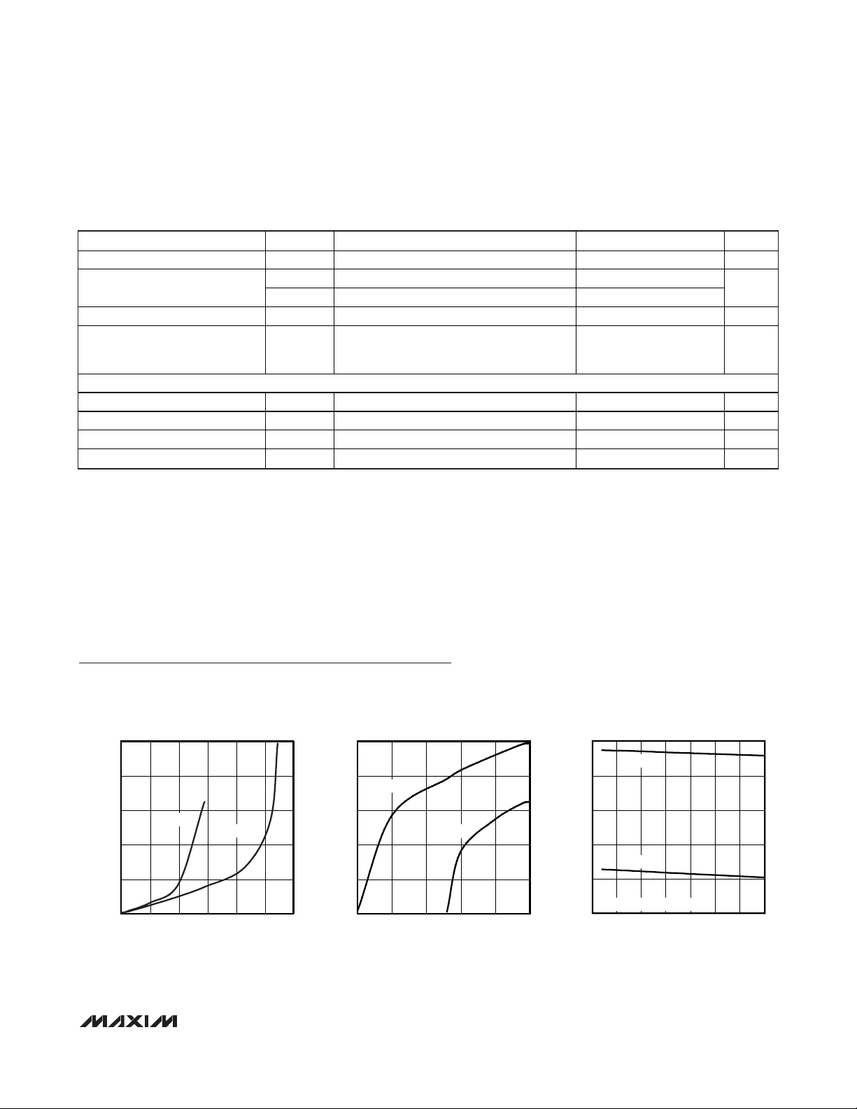
(VCC= 3.3V, TA = +25°C, unless otherwise noted.)
0
1
3
2
4
5
02010 30 40 50 60
RECEIVER OUTPUT LOW VOLTAGE
vs. OUTPUT CURRENT
MAX3280/1/3/4E toc01
OUTPUT CURRENT (mA)
OUTPUT VOLTAGE (V)
VCC = 3.3V
VCC = 5V
0
1
3
2
4
5
-50 -30-40 -20 -10 0
RECEIVER OUTPUT HIGH VOLTAGE
vs. OUTPUT CURRENT
MAX3280/1/3/4E toc02
OUTPUT CURRENT (mA)
OUTPUT VOLTAGE (V)
VCC = 3.3V
VCC = 5V
2.5
3.0
4.0
3.5
4.5
5.0
-50 0-25 25 50 75 100 125
RECEIVER OUTPUT HIGH VOLTAGE
vs. TEMPERATURE
MAX3280/1/3/4E toc03
TEMPERATURE (°C)
RECEIVER OUTPUT HIGH VOLTAGE (V)
VCC = 5V
VCC = 3.3V
VA = 1V, B = GND, IOH = -4mA
Note 2: Parameters are 100% production tested at +25°C, limits over temperature are guaranteed by design.
Note 3: All currents into the device are positive; all currents out of the device are negative. All voltages are referenced to device
ground, unless otherwise noted.
Note 4: V
CM
is the common-mode input voltage. VIDis the differential input voltage.
Note 5: Not production tested. Guaranteed by design.
Note 6: See Table 2 for MAX3284E data rates with V
L
< VCC.
PARAMETER S YMBOL CONDITIONS MIN TYP MAX UNITS
Maximum Data Rate f
Receiver Propagation Delay
Receiver Output |t
PLH
- t
| t
PHL
Device-to-Device Propagation
Delay Matching
ENABLE/DISABLE TIME FOR MAX3281E/MAX3283E
Receiver Enable to Output Low t
Receiver Enable to Output High t
Receiver Disable Time from Low t
Receiver Disable Time from High t
CL = 15pF (Notes 5, 6) 52 Mbps
MAX
t
Figure 1, CL = 15pF, VID = 2V, VCM = 0V 7 15
PLH
t
Figure 1, CL = 15pF, VID = 2V, VCM = 0V 8 15
PHL
Figure 1, CL = 15pF, TA = +25°C 2 ns
PSKEW
Same power supply, maximum
temperature d ifference between
8 ns
devices = +30°C.
Figure 2, CL = 15pF 500 ns
PRZL
Figure 2, CL = 15pF 500 ns
PRZH
Figure 2, CL = 15pF 500 ns
PRLZ
Figure 2, CL = 15pF 500 ns
PRHZ
ns
Page 4

MAX3280E/MAX3281E/MAX3283E/MAX3284E
±15kV ESD-Protected 52Mbps, 3V to 5.5V, SOT23
RS-485/RS-422 True Fail-Safe Receivers
4 _______________________________________________________________________________________
Typical Operating Characteristics (continued)
(VCC= 3.3V, TA = +25°C, unless otherwise noted.)
RECEIVER OUTPUT LOW VOLTAGE
vs. TEMPERATURE
200
150
100
50
RECEIVER OUTPUT LOW VOLTAGE (mV)
0
VCC = 3.3V
VCC = 5V
A = GND, VB = 1V, IOL = 4mA
-50 0-25 25 50 75 100 125
TEMPERATURE (°C)
SUPPLY CURRENT vs. TEMPERATURE
9
8
7
SUPPLY CURRENT (mA)
6
5
-50 25 50-25 0 75 100 125
MAX3280/1/3/4E toc04
VCC = 5V
VCC = 3.3V
TEMPERATURE (°C)
RECEIVER PROPAGATION DELAY (t
vs. TEMPERATURE
9
8
7
(ns)
PLH
t
6
5
4
-50 0-25 25 50 75 100 125
VCC = 5V
VCC = 3.3V
TEMPERATURE (°C)
MAX3280/1/3/4E toc07
PLH
)
RECEIVER PROPAGATION DELAY (t
vs. TEMPERATURE
10
MAX3280/1/3/4E toc05
9
(ns)
8
PHL
t
7
6
-50 0-25 25 50 75 100 125
MAX3284E MAXIMUM DATA RATE
vs. VOLTAGE LOGIC LEVEL
60
50
40
DATA RATE (Mbps)
30
20
1.5 3.52.5 4.5 5.5
VOLTAGE LOGIC LEVEL (V)
VCC = 5V
VCC = 3.3V
TEMPERATURE (°C)
MAX3280/1/3/4E toc08
PHL
)
MAX3280/1/3/4E toc06
SUPPLY CURRENT vs. DATA RATE
10
8
6
4
SUPPLY CURRENT (mA)
2
0
ICC, VCC = VL = 5V
MAX3280/1/3/4E toc09
ICC, VCC = VL = 3.3V
IL, VCC = VL = 5V
IL, VCC = VL = 3.3V
10 1000100 10,000 100,000
DATA RATE (kbps)
10
1
0.1
SUPPLY CURRENT (mA)
L
V
0.01
0.001
-50 25 50-25 0 75 100 125
vs. TEMPERATURE
VCC = VL = 5V
DATA RATE = 52Mbps
VCC = VL = 5V
DATA RATE = 100kbps
TEMPERATURE (°C)
VCC = VL = 3.3V
DATA RATE = 52Mbps
VCC = VL = 3.3V
DATA RATE = 100kbps
MAX3280/1/3/4 toc10
VL SUPPLY CURRENT
Page 5

Detailed Description
The MAX3280E/MAX3281E/MAX3283E/MAX3284E are
single, true fail-safe receivers designed to operate at
data rates up to 52Mbps. The fail-safe architecture guarantees a high output signal if both input terminals are
open or shorted together. See the
True Fail-Safe
section.
This feature assures a stable and predictable output
logic state with any transmitter driving the line. These
receivers function with a 3.3V or 5V supply voltage and
feature excellent propagation delay times (15ns).
The MAX3280E is a single receiver available in a 5-pin
SOT23 package. The MAX3281E (EN, active high) and
MAX3283E (EN, active low) are single receivers that
also contain an enable pin. Both the MAX3281E and
MAX3283E are available in a 6-pin SOT23 package.
The MAX3284E is a single receiver that contains a V
L
pin, which allows communication with low-level logic
included in digital FPGAs. The MAX3284E is available
in a 6-pin SOT23 package.
The MAX3284E’s low-level logic application allows
users to set the logic levels. A logic high level of 1.65V
will limit the maximum data rate to 20Mbps.
±15kV ESD Protection
ESD-protection structures are incorporated on the
receiver input pins to protect against ESD encountered
during handling and assembly. The MAX3280E/
MAX3281E/MAX3283E/MAX3284E receiver inputs (A,
B) have extra protection against static electricity found
in normal operation. Maxim’s engineers developed
state-of-the-art structures to protect these pins against
±15kV ESD without damage. After an ESD event, this
family of parts continues working without latchup.
ESD protection can be tested in several ways. The
receiver inputs are characterized for protection to the
following:
• ±15kV using the Human Body Model
• ±6kV using the Contact Discharge method specified
in IEC 1000-4-2 (formerly IEC 801-2)
• ±12kV using the Air-Gap Discharge method specified in IEC 1000-4-2 (formerly IEC 801-2)
ESD Test Conditions
ESD performance depends on a number of conditions.
Contact Maxim for a reliability report that documents
test setup, methodology, and results.
Human Body Model
Figure 3a shows the Human Body Model, and Figure
3b shows the current waveform it generates when discharged into a low impedance. This model consists of
a 100pF capacitor charged to the ESD voltage of interest, which is then discharged into the device through a
1.5kΩ resistor.
IEC 1000-4-2
Since January 1996, all equipment manufactured
and/or sold in the European community has been
required to meet the stringent IEC 1000-4-2 specification. The IEC 1000-4-2 standard covers ESD testing
and performance of finished equipment; it does not
specifically refer to integrated circuits. The
MAX3280E/MAX3281E/MAX3283E/MAX3284E help
MAX3280E/MAX3281E/MAX3283E/MAX3284E
±15kV ESD-Protected 52Mbps, 3V to 5.5V, SOT23
RS-485/RS-422 True Fail-Safe Receivers
_______________________________________________________________________________________ 5
Pin Description
PIN
MAX3280E MAX3281E MAX3283E MAX3284E
1 1 1 1 V
2 2 2 2 GND Ground
3 3 3 3 RO
4 4 4 4 B Inverting Receiver Input
— — 5 — EN
— 5 — — EN
— — — 5 V
5 6 6 6 A Noninverting Receiver Input
NAME FUNCTION
CC
Positive Supply: 3V VCC 5.5V. Bypass with a 0.1μF
capacitor to GND.
Receiver Output. RO will be high if (V
be low if (V
Receiver Output Enable. Drive EN low to enable RO. When
EN is high, RO is high impedance.
Receiver Output Enable. Drive EN high to enable RO. When
EN is low, RO is high impedance.
Low-Voltage Logic-Level Supply Voltage. VL is a u ser-defined
voltage, ranging from 1.65V to V
L
up to V
- VB) -200mV.
A
. Bypass with a 0.1μF capacitor to GND.
L
- VB) -50mV. RO will
A
. RO output high is pulled
CC
Page 6

MAX3280E/MAX3281E/MAX3283E/MAX3284E
users design equipment that meets Level 3 of IEC 10004-2, without additional ESD-protection components.
The main difference between tests done using the
Human Body Model and IEC 1000-4-2 is higher peak
current in IEC 1000-4-2. Because series resistance is
lower in the IEC 1000-4-2 ESD test model (Figure 4a),
the ESD-withstand voltage measured to this standard is
generally lower than that measured using the Human
Body Model. Figure 4b shows the current waveform for
the ±8kV IEC 1000-4-2 Level 4 ESD Contact Discharge
test. The Air-Gap test involves approaching the device
with a charger probe. The Contact Discharge method
connects the probe to the device before the probe is
energized.
Machine Model
The Machine Model for ESD testing uses a 200pF storage capacitor and zero-discharge resistance. It mimics
the stress caused by handling during manufacturing
and assembly. All pins (not just the RS-485 inputs)
require this protection during manufacturing. Therefore,
the Machine Model is less relevant to the I/O ports than
are the Human Body Model and IEC 1000-4-2.
True Fail-Safe
The MAX3280E/MAX3281E/MAX3283E/MAX3284E
guarantee a logic-high receiver output when the receiver inputs are shorted or open, or when they are connected to a terminated transmission line with all drivers
disabled. This guaranteed logic high is achieved by
setting the receiver threshold between -50mV and
-200mV. If the differential receiver input voltage
(VA- VB) is greater than or equal to -50mV, RO is logic
high. If (VA- VB) is less than or equal to -200mV, RO is
logic low.
In the case of a terminated bus with all transmitters disabled, the receiver’s differential input voltage is pulled
to ground by the termination. This results in a logic high
with a 50mV minimum noise margin. Unlike previous
fail-safe devices, the -50mV to -200mV threshold complies with the ±200mV EIA/TIA-485 standard.
Receiver Enable
(MAX3281E and MAX3283E only)
The MAX3281E and MAX3283E feature a receiver output enable (EN, MAX3281E or EN, MAX3283E) input
that controls the receiver. The MAX3281E receiver
enable (EN) pin is active high, meaning the receiver
outputs are active when EN is high. The MAX3283E
receiver enable (EN) pin is active low. Receiver outputs
are high impedance when the MAX3281E’s EN pin is
low and when the MAX3283E’s EN pin is high.
Low-Voltage Logic Levels
(MAX3284E only)
An increasing number of applications now operate at
low-voltage logic levels. To enable compatibility with
these low-voltage logic level applications, such as digital FPGAs, the MAX3284E VL pin is a user-defined supply voltage that designates the voltage threshold for a
logic high.
At lower VLvoltages, the data rate will also be lower. A
logic-high level of 1.65V will receive data at 20Mbps.
Table 2 gives data rates at various voltages at VL.
Applications Information
Propagation Delay Matching
The MAX3280E/MAX3281E/MAX3283E/MAX3284E
(V
CC
= VL) exhibit propagation delays that are closely
matched from one device to another, even between
devices from different production lots. This feature
allows multiple data lines to receive data and clock signals with minimal skew with respect to each other.
Figure 5 shows the typical propagation delays. Small
receiver skew times, the difference between the low-tohigh and high-to-low propagation delay, help maintain a
symmetrical ratio (50% duty cycle). The receiver skew
time | t
PLH
- t
PHL
| is under 2ns for either a 3.3V supply
or a 5V supply.
Multidrop Clock Distribution
Low package-to-package skew (8ns max) makes the
MAX3280E/MAX3281E/MAX3283E/MAX3284E
(VCC= VL) ideal for multidrop clock distribution. When
distributing a clock signal to multiple circuits over long
transmission lines, receivers in separate locations, and
possibly at two different temperatures, would ideally
±15kV ESD-Protected 52Mbps, 3V to 5.5V, SOT23
RS-485/RS-422 True Fail-Safe Receivers
6 _______________________________________________________________________________________
Table 1. MAX3281E/MAX3283E Enable
Table
Table 2. MAX3284E Data Rate Table
PART ENABLE = HIGH ENABLE = LOW
MAX3281E Active High Z
MAX3283E High Z Active
VCC = 3V TO 5.5V
V
L
1.65V 20Mbps
2.2V 33Mbps
≥3.3V 52Mbps
MAXIMUM DATA RATE
Page 7

provide the same clock to their respective circuits.
Thus, minimal package-to-package skew is critical. The
skew must be kept well below the period of the clock
signal to ensure that all of the circuits on the network
are synchronized.
128 Receivers on the Bus
The standard RS-485 input impedance is 12kΩ (one-
unit load). The standard RS-485 transmitter can drive
32 unit loads. The MAX3280E/MAX3281E/MAX3283E/
MAX3284E present a 1/4-unit-load input impedance
(48kΩ), which allows up to 128 receivers on the bus.
Any combination of these RS-485 receivers with a total
of 32 unit loads can be connected to the same bus.
Thermal Protection
The MAX3280E/MAX3281E/MAX3283E/MAX3284E feature thermal protection. Thermal protection sets the output stage in high-impedance mode when a short circuit
occurs at the output, limiting both the power dissipation
and temperature. The thermal temperature threshold is
+165°C, with a hysteresis of 20°C.
MAX3280E/MAX3281E/MAX3283E/MAX3284E
±15kV ESD-Protected 52Mbps, 3V to 5.5V, SOT23
RS-485/RS-422 True Fail-Safe Receivers
_______________________________________________________________________________________ 7
Test Circuits/Timing Diagrams
Figure 1. Receiver Propagation Delay
Figure 2. MAX3281E/MAX3283E Receiver Enable/Disable Timing
V
OH
RO
V
OL
A
1V
B
-1V
f
= 1MHz
IN
, tf ≤ 3ns
t
r
VCC/2 VCC/2
OUTPUT
t
PHL
INPUT
1.5V
-1.5V
t
PLH
S3
V
ID R
1kΩ
C
L
S1
S2
V
CC
GENERATOR
50Ω
V
CC
S1 OPEN
S2 CLOSED
S3 = 1.5V
0
V
OH
/2
0
V
CC
S1 OPEN
S2 CLOSED
S3 = 1.5V
0
V
OH
0
EN
t
PRZH
OUT
V
/2
CC
EN
t
PRHZ
OUT
0.25V
FOR MAX3281E THE ENABLE SIGNAL IS INVERTED.
VCC/2
V
CC
OUT
OUT
V
CC
0
V
V
V
0
V
V
CC
OL
CC
CC
OL
S1 CLOSED
S2 OPEN
S3 = -1.5V
S1 CLOSED
S2 OPEN
S3 = -1.5V
VCC/2
EN
t
PRZL
/2
V
CC
VCC/2
EN
t
PRLZ
0.25V
Page 8

MAX3280E/MAX3281E/MAX3283E/MAX3284E
±15kV ESD-Protected 52Mbps, 3V to 5.5V, SOT23
RS-485/RS-422 True Fail-Safe Receivers
8 _______________________________________________________________________________________
Test Circuits/Timing Diagrams (continued)
Figure 3a. Human Body ESD Test Model
Figure 3b. Human Body Model Current Waveform
Figure 4a. IEC 1000-4-2 ESD Test Model
Figure 4b. IEC 1000-4-2 ESD Generator Current Waveform
Figure 5. Receiver Propagation Delay Driven by External RS485 Device
HIGH-
VOLTAGE
DC
SOURCE
R
C
1MΩ
CHARGE-CURRENT
LIMIT RESISTOR
C
100pF
s
R
D
1.5kΩ
DISCHARGE
RESISTANCE
STORAGE
CAPACITOR
DEVICE
UNDER
TEST
AMPERES
IP 100%
90%
36.8%
10%
PEAK-TO-PEAK RINGING
I
r
(NOT DRAWN TO SCALE)
0
0
t
RL
TIME
t
DL
CURRENT WAVEFORM
HIGH-
VOLTAGE
DC
SOURCE
R
C
50Ω to 100Ω
CHARGE-CURRENT
LIMIT RESISTOR
C
150pF
s
RD
330Ω
DISCHARGE
RESISTANCE
STORAGE
CAPACITOR
A, 1V/div
DEVICE
UNDER
TEST
I
100%
90%
PEAK
I
10%
tr = 0.7ns to 1ns
30ns
60ns
t
B = GND
10ns
RO, 2.5V/div
Page 9

MAX3280E/MAX3281E/MAX3283E/MAX3284E
±15kV ESD-Protected 52Mbps, 3V to 5.5V, SOT23
RS-485/RS-422 True Fail-Safe Receivers
_______________________________________________________________________________________ 9
Typical Operating Circuit
Pin Configurations
Chip Information
PROCESS: BiCMOS
Package Information
For the latest package outline information and land patterns
(footprints), go to www.maxim-ic.com/packages
. Note that a
“+”, “#”, or “-” in the package code indicates RoHS status only.
Package drawings may show a different suffix character, but
the drawing pertains to the package regardless of RoHS status.
PACKAGE
TYPE
PACKAGE
CODE
OUTLINE
NO.
LAND
PATTERN NO.
5 SOT23 U5+2
21-0057 90-0174
6 SOT23 U6+1
21-0058 90-0175
TOP VIEW
+
15A
V
CC
GND
2
34
TRANSMITTER
DATA IN
MAX3281E/MAX3283E IN REDUNDANT
RECEIVER APPLICATION
120Ω
MAX3280E
SOT23-5
BRO
MAX3283E
EN
MAX3281E
++
16A
V
CC
GND
( ) ARE FOR MAX3283E
MAX3281E
2
MAX3283E
34
SOT23-6
RO1
RO2
16A
V
CC
5
EN (EN)
BRO
GND
MAX3284E
2
34
SOT23-6
5
V
L
BRO
EN
Page 10

MAX3280E/MAX3281E/MAX3283E/MAX3284E
±15kV ESD-Protected 52Mbps, 3V to 5.5V, SOT23
RS-485/RS-422 True Fail-Safe Receivers
Maxim cannot assume responsibility for use of any circuitry other than circuitry entirely embodied in a Maxim product. No circuit patent licenses are
implied. Maxim reserves the right to change the circuitry and specifications without notice at any time.
10
____________________Maxim Integrated Products, 120 San Gabriel Drive, Sunnyvale, CA 94086 408-737-7600
© 2011 Maxim Integrated Products Maxim is a registered trademark of Maxim Integrated Products, Inc.
Revision History
REVISION
NUMBER
0 1/02 Init ial relea se —
1 3/11
REVISION
DATE
DESCRIPTION
Added lead-free parts to the Ordering Information, deleted the transistor count from the
Chip Information section
PAGES
CHANGED
1, 9
 Loading...