

Page 1
现货库存、技术资料、百科信息、热点资讯,精彩尽在鼎好!
General Description
The MAX3275/MAX3277 transimpedance amplifiers
provide a compact low-power solution for communication up to 2.125Gbps. They feature 300nA inputreferred noise at 2.1GHz bandwidth (BW) with 0.85pF
input capacitance. The parts also have 2mA
P-P
AC
input overload.
The MAX3277 is identical to the MAX3275, but with the
output polarities inverted for optimum packaging flexibility. Both parts operate from a single 3.3V supply and
consume only 83mW. The MAX3275/MAX3277 are
compact 24mil x 47mil die and require no external compensation capacitor. A space-saving filter connection is
provided for positive bias to the photodiode through an
on-chip 600Ω resistor to VCC. These features allow
easy assembly into a TO-46 or TO-56 header with a
photodiode.
The MAX3275/MAX3277 and MAX3274 limiting amplifiers provide a two-chip solution for dual-rate, fibre
channel receiver applications.
Applications
Dual-Rate Fibre Channel Optical Receivers
Gigabit Ethernet Optical Receivers
Features
♦ Up to 2.125Gbps (NRZ) Data Rates
♦ 7ps
P-P
Deterministic Jitter for <100µA
P-P
Input Current
♦ 300nA
RMS
Input-Referred Noise at 2.1GHz
Bandwidth
♦ 25mA Supply Current at +3.3V
♦ 2.3GHz Small-Signal Bandwidth
♦ 2.0mA
P-P
AC Overload
♦ Die Size: 24mil x 47mil
MAX3275/MAX3277
Low-Noise, Fibre Channel Transimpedance
Amplifiers
________________________________________________________________ Maxim Integrated Products 1
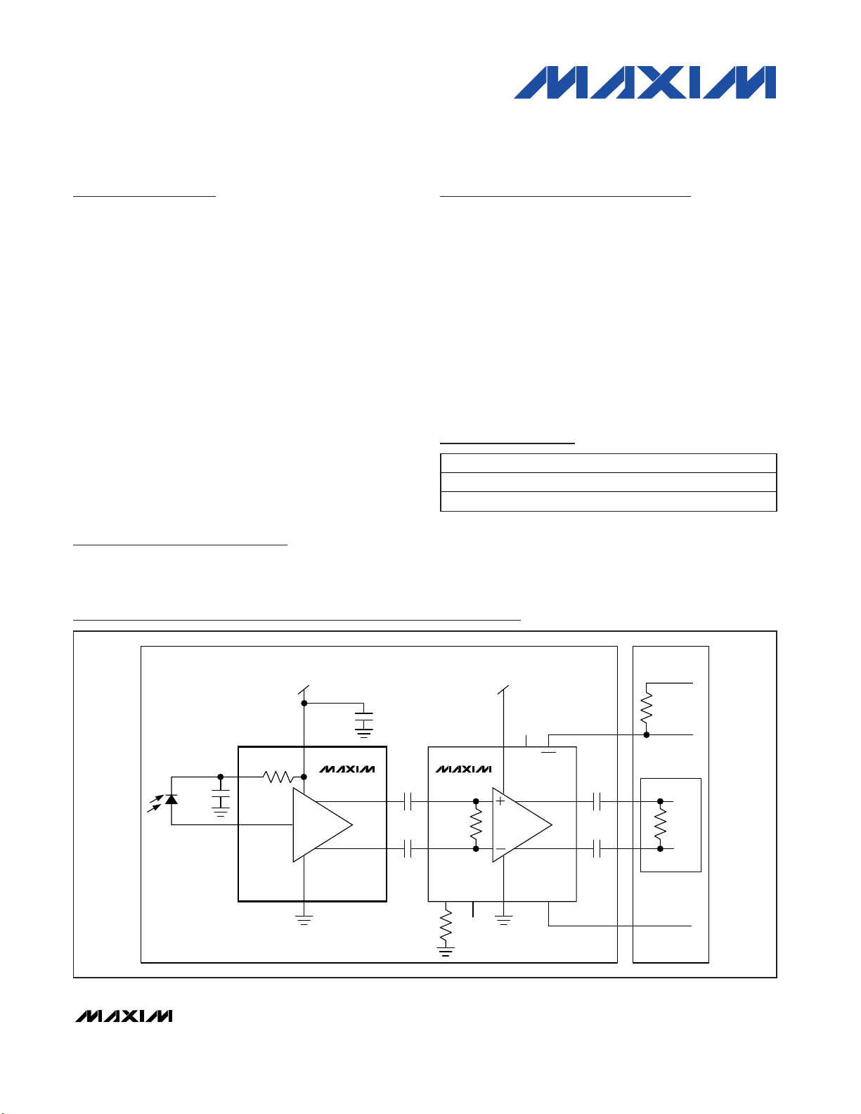
+3.3V
HOST SERVER
OR SWITCH
SMALL FORM FACTOR
OPTICAL RECEIVER
DESERIALIZER
MAX3274
IN+
IN-
TH SQUELCH BWSEL
RATE SELECT
LOS
LIMITING
AMP
OUT+
100Ω
600Ω
660Ω
100Ω
4.7kΩ
TO
10kΩ
0.1µF
0.1µF
0.1µF
0.1µF
OUT-
LOS
+3.3V
MAX3275
IN
GND
V
CC
TIA
OUT+
OUT-
400pF
C
FILTER
400pF
Typical Application Circuit
19-2207; Rev 1; 3/05
For pricing, delivery, and ordering information, please contact Maxim/Dallas Direct! at
1-888-629-4642, or visit Maxim’s website at www.maxim-ic.com.
*Dice are guaranteed to operate from 0°C to +85°C, but are test-
ed only at T
A
= +25°C.
Ordering Information
PART TEMP RANGE PIN-PACKAGE
MAX3275U/D 0°C to +85°C Dice*
MAX3277U/D 0°C to +85°C Dice*
Page 2
MAX3275/MAX3277
Low-Noise, Fibre Channel Transimpedance
Amplifiers
2 _______________________________________________________________________________________
ABSOLUTE MAXIMUM RATINGS
Stresses beyond those listed under “Absolute Maximum Ratings” may cause permanent damage to the device. These are stress ratings only, and functional
operation of the device at these or any other conditions beyond those indicated in the operational sections of the specifications is not implied. Exposure to
absolute maximum rating conditions for extended periods may affect device reliability.
Power-Supply Voltage (VCC).................................-0.5V to +4.0V
Continuous CML Output Current
(OUT+, OUT-) ...............................................-25mA to +25mA
Continuous Input Current (IN)...............................-4mA to +4mA
Continuous Input Current (FILTER).......................-8mA to +8mA
Operating Junction Temperature Range (T
J
) ....-55°C to +150°C
Storage Ambient Temperature Range (T
STG
) ...-55°C to +150°C
Die Attach Temperature...................................................+400°C
ELECTRICAL CHARACTERISTICS
(VCC= +3.0V to +3.6V, TA= 0°C to +85°C. Typical values are at VCC= +3.3V, source capacitance (CIN) = 0.85pF, TA= +25°C,
unless otherwise noted.) (Notes 1, 2)
PARAMETER
CONDITIONS MIN
UNITS
Supply Current I
CC
Including output termination current 25 41 mA
-3dB, CIN = 0.6pF (Note 3) 2.0 2.7 3.3
Small-Signal Bandwidth BW
-3dB, C
IN
= 0.85pF (Note 3) 1.7 2.3 2.7
GHz
Low-Frequency Cutoff -3dB, input current = 40µA (Note 3) 65 kHz
Input Bias Voltage 1.0 V
Input Resistance 40 Ω
CIN = 0.6pF, BW = 0.8GHz (Notes 3, 4) 185 250
CIN = 0.6pF, BW = 1.6GHz (Notes 3, 4) 245 350
CIN = 0.6pF, BW = 2.1GHz (Notes 3, 4) 275 380
CIN = 0.85pF, BW = 0.8GHz (Notes 3, 4) 193 275
CIN = 0.85pF, BW = 1.6GHz (Notes 3, 4) 272 400
Input-Referred Noise I
N
CIN = 0.85pF, BW = 2.1GHz (Notes 3, 4) 300 430
nA
RMS
AC Input Overload (Notes 3, 5) 2
mA
P-P
DC Input Overload (Note 5) 1 mA
Filter Resistance
P-P
510 600 690 Ω
Single-ended
50
Ω
1mA
P-P
< input < 2mA
P-P
(Notes 3, 6, 7) 15 40
100µA
P-P
< input ≤ 1mA
P-P
(Notes 3, 6, 7) 15 31
Deterministic Jitter DJ
10µA
P-P
< input ≤ 100µA
P-P
(Notes 3, 6, 7) 7 16
ps
P-P
Transimpedance Differential output 2.8 3.3 3.8 kΩ
Transimpedance Linear Range 0.95 < linearity < 1.05 (Note 8) 50
µA
P-P
Data Output Swing Input > 100µA
P-P
(Note 9) 220 300 500
mV
P-P
Output Data-Transition Time
Input > 200µA
P-P
, 20% to 80% rise/fall time
(Notes 3, 10)
90 140 ps
Freq ≤ 1GHz 15
Output Return Loss
1GHz < freq ≤ 2GHz 10
dB
f < 1MHz (Note 11) 40
Power-Supply Rejection PSR
1MHz ≤ f < 10MHz (Note 11) 34
dB
SYMBOL
TYP MAX
Output Resistance (OUT+, OUT-)
42.5
57.5
Page 3
MAX3275/MAX3277
Low-Noise, Fibre Channel Transimpedance
Amplifiers
_______________________________________________________________________________________ 3
Note 1: Die parameters are production tested at room temperature only, but are guaranteed by design and characterization from
0°C to +85°C.
Note 2: Source capacitance represents the total capacitance at the IN pad during characterization of the noise and bandwidth
parameters.
Note 3: Guaranteed by design and characterization.
Note 4: Measured using an RF-power meter with no pattern applied at the input. The TIA output is bandwidth limited for
measurement using a 4th-order Bessel Thompson filter. The -3dB frequency of the filter matches the frequency (0.8GHz,
1.6GHz, or 2.1GHz) for the specified noise BW.
Note 5: DC offset and deterministic jitter may exceed specification if AC or DC overload conditions are exceeded.
Note 6: Using fibre channel K28.5± pattern. The input bandwidth is limited to 0.75
✕
(2.125Gbps) by a 4th-order Bessel Thompson
filter. Measured differentially across an AC-coupled 100Ω external load.
Note 7: K28.5± pattern: (00111110101100000101).
Note 8: Gain may vary ±5% relative to reference measured with 30µA
P-P
input.
Note 9: Production tested with 1mA
P-P
input.
Note 10: Using a K28.7 (0011111000) pattern. Measured differentially across an AC-coupled 100Ω external load.
Note 11: Power-supply rejection PSR = -20log(∆V
OUT
/∆VCC), where ∆V
OUT
is the differential output voltage and ∆VCCis the noise
on V
CC
.
ELECTRICAL CHARACTERISTICS (continued)
(VCC= +3.0V to +3.6V, TA= 0°C to +85°C. Typical values are at VCC= +3.3V, source capacitance (CIN) = 0.85pF, TA= +25°C,
unless otherwise noted.) (Notes 1, 2)
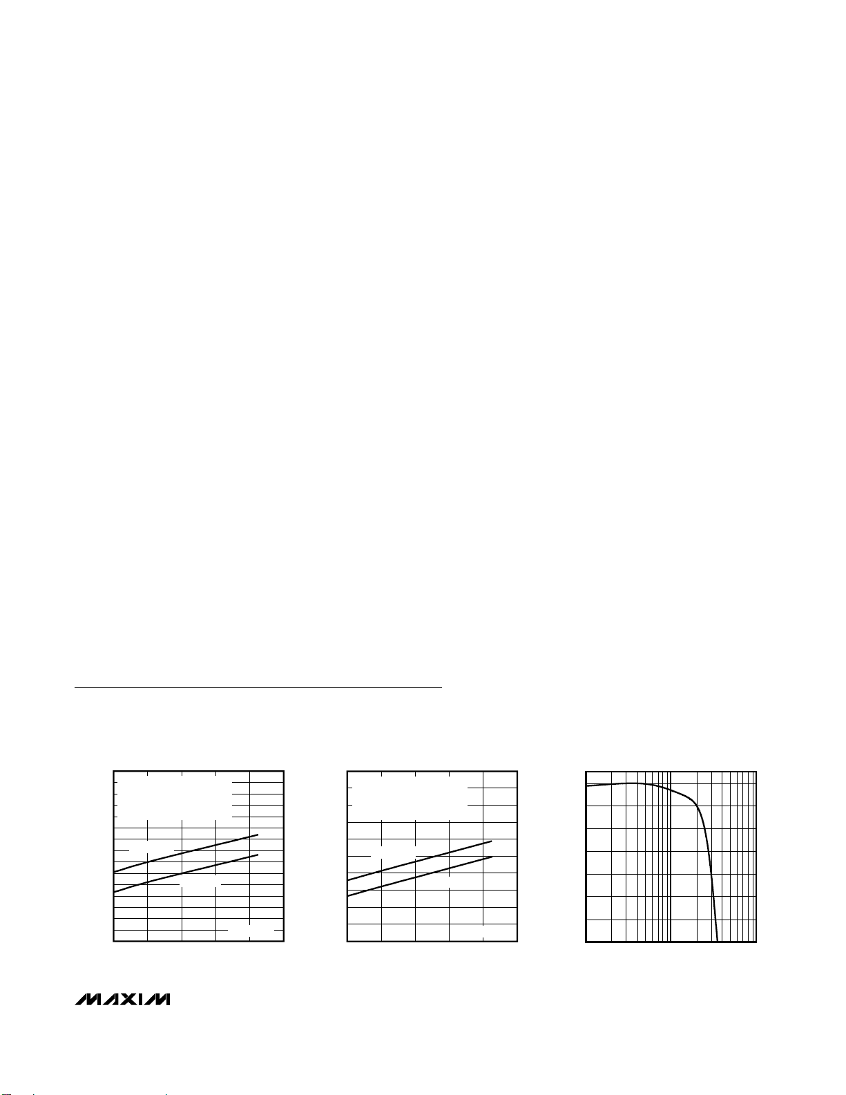
Typical Operating Characteristics
(VCC= +3.3V, CIN= 0.85pF, TA= +25°C, unless otherwise noted.)
INPUT-REFERRED NOISE
vs. TEMPERATURE
MAX3275 toc01
AMBIENT TEMPERATURE (°C)
INPUT-REFERRED NOISE (nA
RMS
)
80604020
210
220
230
240
250
260
270
280
290
300
310
320
330
340
350
200
0100
CIN = 0.85pF
CIN = 0.6pF
CIN IS SOURCE CAPACITANCE
PRESENTED TO DIE, INCLUDING
PIN DIODE, AND PARASITIC
INTERCONNECT CAPACITANCE
BW = 1.6GHz
150
180
170
160
190
200
210
220
230
240
250
04020 60 80 100
INPUT-REFERRED NOISE
vs. TEMPERATURE
MAX3275 toc02
AMBIENT TEMPERATURE (°C)
INPUT-REFERRED NOISE (nA
RMS
)
CIN = 0.85pF
CIN = 0.6pF
C
IN
IS SOURCE CAPACITANCE
PRESENTED TO DIE, INCLUDING
PIN DIODE, AND PARASITIC
INTERCONNECT CAPACITANCE
BW = 0.8GHz
57
100M 1G 10G
FREQUENCY RESPONSE
61
59
MAX3275 toc03
FREQUENCY (Hz)
TRANSIMPEDANCE (dBΩ)
65
63
67
69
71
Page 4

MAX3275/MAX3277
Low-Noise, Fibre Channel Transimpedance
Amplifiers
4 _______________________________________________________________________________________
45
0
0.01 1010.1
DETERMINISTIC JITTER
vs. INPUT AMPLITUDE
15
5
35
25
50
20
10
40
30
MAX3275 toc04
INPUT AMPLITUDE (mA
P-P
)
DETERMINISTIC JITTER (ps
P-P
)
2.125Gbps
K28.5 INPUT
SMALL-SIGNAL TRANSIMPEDANCE
vs. TEMPERATURE
MAX3275 toc05
AMBIENT TEMPERATURE (°C)
TRANSIMPEDANCE (dB
Ω
)
80604020
71
70
69
68
67
66
65
64
63
62
61
72
73
74
60
0 100
2.0
2.3
2.2
2.1
2.4
2.5
2.6
2.7
2.8
2.9
3.0
04020 60 80 100
BANDWIDTH vs. TEMPERATURE
MAX3275 toc06
AMBIENT TEMPERATURE (°C)
BANDWIDTH (GHz)
CIN = 0.85pF
CIN = 0.6pF
EYE DIAGRAM (INPUT = 10µA
P-P
)
MAX3275 toc07
5mV/div
80ps/div
INPUT: K28.5
EYE DIAGRAM (INPUT = 2mA
P-P
)
MAX3275 toc08
50mV/div
80ps/div
INPUT: K28.5
-40
-35
-30
-25
-20
-15
-10
-5
0
01G500M 1.5G 2G 2.5G 3G
DIFFERENTIAL OUTPUT REFLECTION
COEFFICIENT
MAX3275 toc09
FREQUENCY (Hz)
S22 (dB)
0
15
10
5
20
25
30
35
40
45
50
04020 60 80 100
SUPPLY CURRENT vs. TEMPERATURE
MAX3275 toc10
AMBIENT TEMPERATURE (°C)
SUPPLY CURRENT (mA)
-200
-150
-100
-50
0
50
100
150
200
-200 -100 0 100 200
DC TRANSFER FUNCTION
(FILTER = GND)
MAX3275 toc11
INPUT CURRENT (µA)
OUTPUT VOLTAGE (mV)
Typical Operating Characteristics (continued)
(V
CC
= +3.3V, CIN= 0.85pF, TA= +25°C, unless otherwise noted.)
Page 5

Detailed Description
The MAX3275/MAX3277 are transimpedance amplifiers
designed for up to 2.125Gbps fibre channel applications. A functional diagram of the MAX3275/MAX3277 is
shown in Figure 1. The MAX3275/MAX3277 comprises a
transimpedance amplifier stage, a voltage amplifier
stage, an output buffer, and a direct-current feedback
cancellation circuit.
Transimpedance Amplifier Stage
The signal current at the input flows into the summing
node of a high-gain amplifier. Shunt feedback through
the resistor R
F
converts this current to a voltage. In parallel with the feedback are two back-to-back Schottky
diodes that clamp the output signal for large input currents as shown in Figure 2.
Voltage Amplifier Stage
The voltage amplifier stage provides gain and converts
the single-ended input to differential outputs.
MAX3275/MAX3277
Low-Noise, Fibre Channel Transimpedance
Amplifiers
_______________________________________________________________________________________ 5
MAX3275
BOND PAD
MAX3277
NAME FUNCTION
1, 9 1, 9 V
CC
Supply Voltage
2, 5 2, 5 GND Circuit Ground
3 4 OUT- Inverting Data Output. Current flowing into IN causes the voltage at OUT- to decrease.
4 3 OUT+
Noninverting Data Output. Current flowing into IN causes the voltage at OUT+ to
increase.
6 6 N.C. No Connection. Not internally connected.
7 7 FILTER
Provides bias voltage for the photodiode through a 600Ω resistor to V
CC
. When
grounded, this pin disables the DC cancellation amplifier to allow a DC path from IN to
OUT+ and OUT- for testing.
8 8 IN TIA Input. Signal current from photodiode flows into this pin.
Pad Description
VOLTAGE
AMPLIFIER
TIA
OUTPUT
BUFFER
OUT+
50Ω 50Ω
OUT-
V
CC
V
CC
R
f
V
CC
LOWPASS
FILTER
600Ω
FILTER
IN
GND
DC CANCELLATION
DISABLE
MAX3275
MAX3277
Figure 1. Functional Diagram
BOND PAD
Page 6

MAX3275/MAX3277
Output Buffer
The output buffer provides a reverse-terminated voltage
output. The buffer is designed to drive a 100Ω differen-
tial load between OUT+ and OUT-. The output current
is divided between internal 50Ω resistors and the exter-
nal load resistor.
For optimum supply-noise rejection, the MAX3275/
MAX3277 should be terminated with a differential load.
If a single-ended output is required, the unused
output should be terminated in a similar manner. The
MAX3275/MAX3277 will not drive a DC-coupled, 50Ω
grounded load; however, it will drive a compatible 50Ω
CML input.
DC Cancellation Circuit
The direct-current (DC) cancellation circuit uses lowfrequency feedback to remove the DC component of
the input signal (Figure 3). This feature centers the
input signal within the transimpedance amplifier’s linear
range, thereby reducing pulse-width distortion caused
by large input signals. Pulse-width distortion in small
signals will not be corrected.
The DC cancellation circuit is internally compensated
and therefore does not require external capacitors. This
circuit minimizes pulse-width distortion for data
sequences that exhibit a 50% mark density and 8b/10b
coding. A mark density significantly different from 50%
will cause the MAX3275/MAX3277 to generate pulsewidth distortion.
DC cancellation current is drawn from the input and
creates noise. For low-level signals with little or no DC
component, the added noise is insignificant.
Applications Information
Optical Power Relations
Many of the MAX3275/MAX3277 specifications relate to
the input signal amplitude. When working with optical
receivers, the input is sometimes expressed in terms of
average optical power and extinction ratio. Figure 4 and
Table 1 show relations that are helpful for converting
optical power to input signal when designing with
the MAX3275/MAX3277. (Refer to Application note
HFAN–3.0.0 Accurately Estimating Optical Receiver
Sensitivity.)
Optical Sensitivity Calculation
The input-referred RMS noise current (IN) of the
MAX3275/MAX3277 generally determines the receiver
Low-Noise, Fibre Channel Transimpedance
Amplifiers
6 _______________________________________________________________________________________
AMPLITUDE
OUTPUT (LARGE SIGNALS)
TIME
OUTPUT (SMALL SIGNALS)
Figure 2. MAX3275/MAX3277 Limited Output
AMPLITUDE INPUT FROM PHOTODIODE
TIME
INPUT (AFTER DC CANCELLATION)
Figure 3. DC Cancellation Effect on Input
Table 1. Optical Power Relations
PARAMETER
RELATION
Average Power P
AVG
P
AVG
= (P0 + P1)/2
Extinction Ratio r
e
re = P1/P
0
Optical Power of a 1
P
1
P1 = 2P
AVG(re
)/(re + 1)
Optical Power of a 0
P
0
P0 = 2P
AVG
/(re + 1)
Signal Amplitude P
IN
PIN = P1 - P
0
PIN = 2P
AVG(re
- 1)/(re + 1)
Figure 4. Optical Power Relations
P
1
P
AVG
OPTICAL POWER
P
0
SYMBOL
TIME
Page 7

sensitivity. To obtain a system bit error rate (BER) of 1E12, the signal-to-noise ratio must always exceed 14.1.
The input sensitivity, expressed in average power, can
be estimated as:
where ρ is the photodiode responsivity in A/W and INis
RMS current in Amps.
Input Optical Overload
The overload is the largest input that the MAX3275/
MAX3277 accept while meeting specifications. The
optical overload can be estimated in terms of average
power with the following equation:
Optical Linear Range
The MAX3275/MAX3277 have high gain, which limits
the output when the input signal exceeds 50µA
P-P
. The
MAX3275/MAX3277 operate in a linear range (10% linearity) for inputs not exceeding:
Layout Considerations
Noise performance and bandwidth will be adversely
affected by capacitance at the IN pad. Minimize
capacitance on this pad and select a low-capacitance
photodiode. Assembling the MAX3275/MAX3277 in die
form using chip and wire technology provides the best
possible performance. Figure 5 shows a suggested layout for a TO header for the MAX3275/MAX3277.
Special care should be taken to ensure that ESD at IN
does not exceed 500V.
Photodiode Filter
Supply voltage noise at the cathode of the photodiode
produces a current I = CPD∆V/∆t, which reduces the
receiver sensitivity (CPDis the photodiode capacitance). The filter resistor of the MAX3275/MAX3277,
combined with an external capacitor, can be used to
reduce this noise (see the Typical Application Circuit).
Current generated by supply noise voltage is divided
between C
FILTER
and CPD. The input noise current due
to supply noise is (assuming the filter capacitor is much
larger than the photodiode capacitance):
I
NOISE
= (V
NOISE
)(CPD) / (R
FILTER
)(C
FILTER
)
If the amount of tolerable noise is known, the filter
capacitor can be easily selected:
C
FILTER
= (V
NOISE
)(CPD) / (R
FILTER
)(I
NOISE
)
For example, with maximum noise voltage = 100mV
P-P
,
CPD= 0.85pF, R
FILTER
= 600Ω, and I
NOISE
selected to
be 350nA:
C
FILTER
= (100mV)(0.85pF) / (600Ω)(350nA) = 400pF
Wire Bonding
For high-current density and reliable operation, the
MAX3275/MAX3277 use gold metalization. Connections
to the die should be made with gold wire only, using
ball-bonding techniques. Wedge bonding is not recommended. Die thickness is typically 15 mils (0.4mm).
Linear Range=10 log
50E - 6 r +1 1000
2(r-1)
e
e
()()
×
ρ
dBm
Overload= 10 log
2E - 3 r +1 1000
2(r-1)
e
e
()()
×
ρ
dBm
Sensitivity=10 log
14.1I (r +1) 1000
2(r-1)
Ne
e
×
ρ
dBm
MAX3275/MAX3277
Low-Noise, Fibre Channel Transimpedance
Amplifiers
_______________________________________________________________________________________ 7
CASE IS GROUND OUTPUT POLARITIES
REVERSED FOR MAX3277
C
FILTER
V
CC
PHOTODIODE
MAX3275
OUT-
CAP
OUT+
Figure 5. Suggested Layout for TO-46 Header
Pad Coordinates
PAD# COORDINATES (µm)
1 16, 39
2 16, 372
3 16, 806
4 358, 806
5 358, 341
6 358, 36
7 362, -116
8 250, -116
9 138, -116
Page 8

MAX3275/MAX3277
Low-Noise, Fibre Channel Transimpedance
Amplifiers
8 _______________________________________________________________________________________
Chip Topographies
0.024"
(0.6mm)
GND
(PAD 2)
V
CC
(PAD 1)
INDEX
V
CC
(PAD 9)IN(PAD 8)
OUT-
(PAD 3)
OUT+
(PAD 4)
GND
(PAD 5)
N.C.
(PAD 6)
FILTER
(PAD 7)
0.047"
(1.2mm)
MAX3275
Page 9

MAX3275/MAX3277
Low-Noise, Fibre Channel Transimpedance
Amplifiers
Maxim cannot assume responsibility for use of any circuitry other than circuitry entirely embodied in a Maxim product. No circuit patent licenses are
implied. Maxim reserves the right to change the circuitry and specifications without notice at any time.
Maxim Integrated Products, 120 San Gabriel Drive, Sunnyvale, CA 94086 408-737-7600 _____________________ 9
© 2005 Maxim Integrated Products Printed USA is a registered trademark of Maxim Integrated Products, Inc.
0.024"
(0.6mm)
GND
(PAD 2)
V
CC
(PAD 1)
INDEX
V
CC
(PAD 9)IN(PAD 8)
OUT+
(PAD 3)
OUT-
(PAD 4)
GND
(PAD 5)
N.C.
(PAD 6)
FILTER
(PAD 7)
0.047"
(1.2mm)
MAX3277
Chip Topographies (continued)
Chip Information
TRANSISTOR COUNT: 301
SUBSTRATE: ISOLATED
PROCESS: SiGe BIPOLAR
 Loading...