

Page 1
现货库存、技术资料、百科信息、热点资讯,精彩尽在鼎好!
General Description
The MAX3274 dual-rate Fibre Channel limiting amplifier
is optimized for use in dual-rate 2.125Gbps/1.0625Gbps
Fibre Channel optical receiver systems. An on-chip
selectable fourth-order Bessel Thompson filter offers
15dB (typ) of attenuation at 2GHz to suppress the relaxation oscillation (RO) found in legacy transmitters. The
amplifier accepts a wide range of input voltages and
provides constant-level output voltages with controlled
edge speeds. Receivers using the MAX3275/MAX3277
transimpedance amplifiers (TIA) and the MAX3274 dualrate limiting amplifier can meet the Fibre Channel receiver sensitivity optical modulation amplitude (OMA)
specification of 49mW
P-P
at 2.125Gbps and 31mW
P-P
at
1.0625Gbps. Additional features include a programmable threshold loss-of-signal (LOS) detector, output
squelch, and bandwidth select. The MAX3274 features
current-mode logic (CML) data outputs. The MAX3274 is
available in a 16-pin QFN package, making it ideal for
GBIC and small form-factor receiver modules.
Applications
Fibre Channel GBIC Optical Modules
Dual-Rate Fibre Channel SFF/SFP Optical
Modules
Features
♦ Dual-Rate 1.0625Gbps/2.125Gbps Operation
♦ On-Chip Selectable 4th-Order Filter
♦ Relaxation Oscillation Suppression of Legacy,
CD Laser-Based Transmitters
♦ Available in a 100Ω Output Termination
♦ Programmable Loss-of-Signal (LOS) Threshold
♦ Output Squelch Control
♦ Power-On Reset Minimizes Inrush Current
♦ 4mm
✕
4mm 16-Pin QFN Package
MAX3274
Dual-Rate Fibre Channel Limiting Amplifier
________________________________________________________________ Maxim Integrated Products 1
Ordering Information
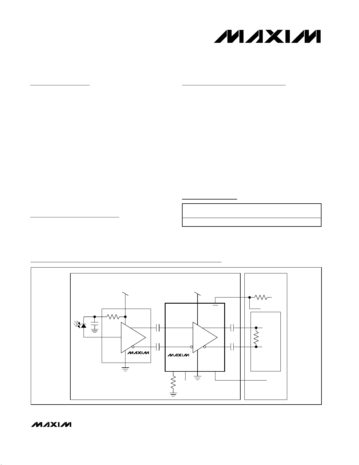
TIA
+3.3V
V
CC
RATE SELECT
DESERIALIZER
IN+
RX LOS
IN-
0.1µF
OUT+
OUT-
TH SQUELCH BWSELGND
LOSLOS
4.7kΩ TO 10kΩ
0.1µF
OPTICAL MODULE
RECEIVER SECTION
HOST
SERVER OR SWITCH
HOST V
CC
100Ω
OR 150Ω
+3.3V
MAX3274
0.1µF
0.1µF
MAX3275
Typical Operating Circuit
19-2375; Rev 1; 7/03
For pricing, delivery, and ordering information, please contact Maxim/Dallas Direct! at
1-888-629-4642, or visit Maxim’s website at www.maxim-ic.com.
Pin Configurations appear at end of data sheet.
MAX3274UGE 0°C to +85°C 16 QFN G1644-1
PART TEMP RANGE PIN-PACKAGE
PKG.
CODE
Page 2
MAX3274
Dual-Rate Fibre Channel Limiting Amplifier
2 _______________________________________________________________________________________
ABSOLUTE MAXIMUM RATINGS
ELECTRICAL CHARACTERISTICS
(VCC= +3.0V to +3.6V, TA= 0°C to +85°C. Typical values are at VCC= +3.3V and TA= +25°C, unless otherwise noted.)
Stresses beyond those listed under “Absolute Maximum Ratings” may cause permanent damage to the device. These are stress ratings only, and functional
operation of the device at these or any other conditions beyond those indicated in the operational sections of the specifications is not implied. Exposure to
absolute maximum rating conditions for extended periods may affect device reliability.
Supply Voltage (VCC) ............................................-0.5V to +6.0V
Continuous CML Output Current
(OUT+, OUT-) ...............................................-25mA to +25mA
CML Input Voltage (IN+, IN-) .....................-0.5V to (V
CC
+ 0.5V)
Differential Input Voltage (IN+, IN-).....................................2V
P-P
TTL Input Voltage
(BWSEL, SQUELCH, TEST)....................-0.5V to (V
CC
+ 0.5V)
Voltage at TH ................................................-0.5V to V
CC
+ 0.5V
Current into TH...................................................................5.0mA
Open Collector (LOS, LOS)...................................-0.5V to +5.5V
Operating Ambient Temperature Range .............-40°C to +85°C
Storage Ambient Temperature Range...............-55°C to +100°C
1
Supply Current 78 99 mA
Data Rate
BWSEL Response Time (Note 2) 10 µs
Input Range V
Random Jitter
Total Jitter
LOS, LOS Transition Time 10% to 90% rise/fall time (Notes 2, 7) 5 350 ns
LOS, LOS Response Time Figure 1 (Note 2) 1 20 µs
LOS, LOS Hysteresis
LOS Assert (V
LOS Assert (V
Squelch Input Current 100 µA
Single-Ended Input Resistance R
Data Input VSWR f < 2GHz (Note 2) 2.5
Differential Output Resistance R
CML Output Voltage V
Data Output Levels SQUELCH = 1, VIN < V
PARAMETER SYMBOL CONDITIONS MIN TYP MAX UNITS
BWSEL = 0 1.0625
BWSEL = 1 2.125
-3dB, BWSEL = 0 (Note 1) 0.77 0.89 1.0
-15dB, BWSEL = 0 (Note 1) 2.0Small-Signal Bandwidth
-3dB, BWSEL = 1 (Note 1) 1.7
(Notes 2, 3) 10 1200 mV
IN
BWSEL = 0, 10mV ≤ input ≤ 20mV (Notes 2, 4) 44 60
BWS E L = 0, 20m V < i np ut ≤ 1200m V ( N otes 2, 4) 37 44Deterministic Jitter
BWS E L = 1, 10m V ≤ i np ut ≤ 1200m V ( N otes 2, 4) 10 20
BWSEL = 0 (Notes 2, 5) 5.1
BWSEL = 1 (Notes 2, 5) 2.8
BWSEL = 0 (Note 6) 117
BWSEL = 1 (Note 6) 49
20 ✕ log (V
DEASSERT/VASSERT
(Note 8)
= 30mV
V
TH
) Range 330Ω < RTH < 2.0kΩ (Notes 2, 8) 8 30 mV
LOS
) Error 330Ω < RTH < 2.0kΩ (Notes 2, 8) -30 +30 %
LOS
IN+, IN- to V
IN
OUT+ to OUT- (MAX3274) 80 100 120 Ω
OUT
SQUELCH = 0 (Note 4) 900 1200 1600
OUT
SQUELCH = 1, VIN < V
P-P
CC
), VTH = 6mV
P-P
28
(Notes 2, 8) 4 8
40 50 60 Ω
(Note 4) 30
TH
(Note 4) V
TH
CC
- 0.
V
CC
Gbps
GHz
P-P
ps
P-P
ps
RMS
ps
P-P
dB
mV
P-P
V
Page 3
MAX3274
Dual-Rate Fibre Channel Limiting Amplifier
_______________________________________________________________________________________ 3
ELECTRICAL CHARACTERISTICS (continued)
(VCC= +3.0V to +3.6V, TA= 0°C to +85°C. Typical values are at VCC= +3.3V and TA= +25°C, unless otherwise noted.)
Note 1: Measured with a ≤-50dBm input signal on a network analyzer.
Note 2: Specifications are guaranteed by design and characterization.
Note 3: Using 2
7
- 1 PRBS pattern. The input bandwidth is limited to 0.75 ✕(selected data rate) by a 4th-order Bessel Thompson filter.
Note 4: Using a K28.5 pattern at the selected bit rate. Measured differentially into a matched external load.
Note 5: Using a K28.7 or equivalent pattern at the selected bit rate. Measured over the entire input voltage range.
Note 6: Total jitter is estimated as TJ = DJ + 14 x RJ, where DJ is the peak-to-peak deterministic jitter, and RJ is the RMS random jitter.
Note 7: LOS (open collector) is connected to a +5.5V supply through a 4.7kΩ external resistor.
Note 8: Using K28.7 or equivalent pattern at selected bit rate.
Note 9: Total jitter, deterministic jitter, LOS hysteresis, LOS assert performance verified.
Data Output Edge Speed
LOS Current Sink
LOS Current Sink
LOS, LOS Output Low Voltage LOS, LOS sink current = 1mA 0.5 V
Supply Noise Tolerance
PARAMETER SYMBOL CONDITIONS MIN TYP MAX UNITS
20% to 80%, BWSEL = 0 (Notes 2, 5) 170 220
20% to 80%, BWSEL = 1 (Notes 2, 5) 105 140
LOS asserted 1.0 mA
LOS not asserted, V
+5.5V
LOS not asserted 1.0 mA
LOS asserted, V
10kHz ≤ f < 1MHz (Note 9) 40
1MHz ≤ f < 50MHz (Note 9) 20
= 0, 4.7kΩ pullup to
CC
= 0, 4.7kΩ pullup to +5.5V 0 10 µA
CC
010µA
ps
mV
P-P
P-P
Page 4

MAX3274
Dual-Rate Fibre Channel Limiting Amplifier
4 _______________________________________________________________________________________
Typical Operating Characteristics
(VCC= +3.3V, TA= +25°C, unless otherwise noted.)
INPUT = 1.2V
P-P
, 27 - 1 PRBS, BWSEL = 1
MAX3274/76 toc01
100ps/div
150mV/div
INPUT = 10mV
P-P
, 27 - 1 PRBS, BWSEL = 1
MAX3274/76 toc02
100ps/div
150mV/div
INPUT = 1.2V
P-P
, 27 - 1 PRBS, BWSEL = 0
MAX3274/76 toc03
200ps/div
150mV/div
MAX3274/76 toc04
200ps/div
150mV/div
INPUT = 10mV
P-P
, 27 - 1 PRBS, BWSEL = 0
INPUT RELAXATION OSCILLATION
(RO) OF LEGACY
FIBRE CHANNEL TRANSMITTERS
(INPUT = K28.5, 1.0625Gbps)
MAX3274/76 toc05
200ps/div
1mV/div
MAX3274/76 toc06
200ps/div
140mV/div
BWSEL = 1
RO NOT SUPPRESSED
BWSEL = 0
RO FULLY SUPPRESSED
MAX3274/76 toc07
200ps/div
140mV/div
Page 5

SUPPLY CURRENT vs. TEMPERATURE
MAX3274/76 toc9
TEMPERATURE (°C)
SUPPLY CURRENT (mA)
80604020
20
40
60
80
100
120
140
160
180
200
0
0100
MAX3274
Dual-Rate Fibre Channel Limiting Amplifier
_______________________________________________________________________________________ 5
Typical Operating Characteristics (continued)
(VCC= +3.3V, TA= +25°C, unless otherwise noted.)
1400
1200
)
P-P
1000
800
600
400
DIFFERENTIAL OUTPUT (mV
200
0
0
-5
-10
-15
-20
-25
GAIN (dB)
-30
-35
-40
-45
-50
1G 10G
TRANSFER FUNCTION
MAX3274/76 toc08
025
DIFFERENTIAL INPUT (mV
INPUT DIFFERENTIAL RETURN GAIN
2015105
)
P-P
OUTPUT DIFFERENTIAL RETURN GAIN
(SIGNAL LEVEL of -60dBm)
5
0
MAX3274/76 toc11
FREQUENCY (Hz)
-5
-10
-15
-20
GAIN (dB)
-25
-30
-35
-40
1G 10G
(SIGNAL LEVEL of -60dBm)
FREQUENCY (Hz)
50
44
38
32
26
20
GAIN
14
-10
70
60
)
P-P
MAX3274/76 toc12
50
40
30
20
LOS ASSERT/DEASERT (mV
10
FORWARD DIFFERENTIAL GAIN
(INPUT LEVEL of -60dBm, BWSEL = 0)
8
2
-4
1G
FREQUENCY (Hz)
ASSERT/DEASSERT LEVELS vs. R
(BWSEL = 1, 2.125Gbps, K28.5)
DEASSERT
ASSERT
0
0 3000
RTH (Ω)
2500200015001000500
MAX3274/76 toc10
10G100M
TH
MAX3274/76 toc13
LOS HYSTERESIS vs. TEMPERATURE
(BWSEL = 1, 2.125Gbps, K28.5)
10
9
8
7
6
5
4
HYSTERESIS (dB)
3
2
1
0
0 100
Ω
RTH = 680
TEMPERATURE (°C)
Ω
RTH = 330
Ω
RTH = 1.8k
80604020
MAX3274/76 toc14
50
45
)
40
P-P
35
30
25
20
15
DETERMINISTIC JITTER (ps
10
5
0
DETERMINISTIC JITTER
14
MAX3274/76 toc15
BWSEL = 0
BWSEL = 1
01000
DIFFERENTIAL INPUT (mV
900800600 700200 300 400 500100
)
P-P
12
)
10
RMS
8
6
4
RANDOM JITTER (ps
2
0
0200
RANDOM JITTER
BWSEL = 0
BWSEL = 1
DIFFERENTIAL INPUT (mV
MAX3274/76 toc16
18016014012010080604020
)
P-P
Page 6

MAX3274
Dual-Rate Fibre Channel Limiting Amplifier
6 _______________________________________________________________________________________
Pin Description
PIN NAME FUNCTION
1 IN+ Noninverted Data Input
2 IN- Inverted Data Input
3, 7, 10 V
4 BWSEL
CC
5 TEST Test Pin Should Be Connected to Ground
6 SQUELCH
8, 13, 16 GND Supply Ground
9TH
11 OUT- Inverted Data Output
12 OUT+ Noninverted Data Output
14 LOS
15 LOS
EP
Exposed
Pad
Supply Voltage
Bandwidth Select Pin. When BWSEL is set to a TTL-low level or left open, a 4th-order Bessel
Thompson filter suppresses relaxation oscillations from legacy CD laser transmitters. Connect
BWSEL to a TTL-high for operation above 1.0625Gbps.
Squelch Input. The squelch function is disabled when SQUELCH is set to a TTL-low. When
SQUELCH is set to a TTL-high level, and LOS is asserted, the data outputs (OUT+ and OUT-) are
forced to static levels.
Loss-of-Signal Threshold. A resistor connected from this pin to ground sets the input signal level at
which the loss-of-signal (LOS) outputs are asserted. See the Typical Operating Characteristics and
Design Procedure sections for more information.
Inverted Loss-of-Signal Output. LOS is high when the level of the input signal is above the preset
threshold set by the TH pin. LOS is asserted low when the input signal level drops below the
threshold.
Loss-of-Signal Output. LOS is low when the level of the input signal is above the preset threshold
set by the TH pin. LOS is asserted high when the input signal level drops below the threshold.
Ground. The exposed paddle must be soldered to the circuit board ground for proper thermal and
electrical performance.
Page 7

Detailed Description
Figure 2 is a functional diagram of the MAX3274 limiting amplifier. Typical gain is 46dB. A linear input drives
a bandwidth selector. An offset correction loop with
lowpass filtering ensures low deterministic jitter. An
integrated RMS signal detector monitors for loss-of-signal conditions. The output buffer provides a limited
CML output signal.
Input Buffer
The MAX3274 input buffer (Figure 3) provides a 100Ω
input impedance between IN+ and IN-. DCcoupling the inputs is not recommended; doing so prevents proper functioning of DC offset correction circuitry.
Signal Detect and Loss-of-Signal
An RMS signal detector looks at the signal from the
input buffer and compares it to a threshold set by a
resistor at pin TH. The status of the signal-detect information appears at the LOS outputs. These are opencollector outputs and require external pullup resistors
connected to the host power supply. The LOS outputs
are high impedance when the power supply to the
MAX3274 is 0V. ESD protection on the dual-rate limiting
amplifiers’ LOS outputs do not forward-bias when the
power supply of the MAX3274 is 0V or below the host
power supply.
Offset Correction
A low-frequency feedback loop is integrated into the
limiting amplifiers to reduce input offset and thereby
minimize duty-cycle distortion. For proper operation,
the input must be externally AC-coupled. The offset
correction circuit has been optimized for the Fibre
Channel character set, disparity rules, and 8b/10b data
encoding. This dictates an average data input mark
density of 50% and a maximum run length of five consecutive identical digits (CID) or bits.
CML Output Buffer
The MAX3274 CML outputs (Figure 4) provide high tolerance to impedance mismatches and inductive connectors. The output current is approximately 24mA. The
squelch function is enabled when SQUELCH is set to a
TTL-high level or connected to VCC. The squelch function holds OUT+ and OUT- at a static voltage when the
input signal level drops below the loss-of-signal threshold. The output buffer can be AC- or DC-coupled to the
load. For DC operation, the load must be terminated to
VCCof the MAX3274.
Design Procedure
Programming the LOS Assert Threshold
External resistor RTHprograms the loss-of-signal
threshold. See the LOS Threshold vs. RTHgraph in the
Typical Operating Characteristics section. RTHcan be
estimated by RTH= 15 / VTH, where VTHis the peak-topeak differential input assert level.
Selecting the AC-Coupling Capacitors
The input and output AC-coupling capacitors (CIN,
C
OUT
) should be selected to minimize the receiver’s
deterministic jitter. Lowering the low-frequency cutoff
reduces deterministic jitter. The low-frequency cutoff
can be determined by:
where RLis the single-ended load impedance and R
S
is the single-ended source impedance. CIN, C
OUT
=
0.1µF is recommended.
Applications Information
Optical Hysteresis
In an optical receiver, the electrical power change at
the limiting amplifier is 2 times the optical power
change. For example, if a receiver’s optical input power
(χ) increases by a factor of 2, and the preamplifier is
linear, then the voltage input to the limiting amplifier
also increases by a factor of 2. The optical power
change is 10log (2χ/χ) = 10log(2) = 3dB. At the limiting
amplifier, the electrical power change is:
The typical voltage hysteresis for the MAX3274 is 6dB.
This provides an optical hysteresis of 3dB.
MAX3274
Dual-Rate Fibre Channel Limiting Amplifier
_______________________________________________________________________________________ 7
Figure 1. LOS Response Time
V
DEASSERT
V
IN
LOS, LOS
OUTPUTS
V
ASSERT
50
LOS RESPONSE TIME
50
f
=
C
2π
1
CRR
×× +
()
LS
10
log
2
2
/
VR
()
IN IN
2
/
VR
IN IN
=
10 2 20 2 6
2
log log
=
()
=
()
dB
Page 8

MAX3274
Dual-Rate Fibre Channel Limiting Amplifier
8 _______________________________________________________________________________________
Figure 2. Functional Diagram of the MAX3274 Limiting Amplifier
Figure 4. CML Output Circuit
Figure 3. Input Circuit
OFFSET
CORRECTION
LPF
4TH-ORDER
LP FILTER
IN+
IN-
BWSEL
TH
SQUELCH
V
CC
50Ω 50Ω
IN+
0
1
RMS
SIGNAL
DETECT
V
CC
50Ω/75Ω 50Ω/75Ω
OUT+
OUT-
LOS
LOS
OUT+
OUT-
IN-
ESD
STRUCTURES
DATA
ESD
STRUCTURES
Page 9

MAX3274
Dual-Rate Fibre Channel Limiting Amplifier
_______________________________________________________________________________________ 9
Pin Configuration
Chip Information
DEVICE COUNT: 2855
TRANSISTOR COUNT: 1310
PROCESS: BiPOLAR: SiGe, SOI
TOP VIEW
IN+
IN-
V
BWSEL
GND
LOS
LOS
GND
13
14
15
16
12
1
2
3
CC
4
EXPOSED PAD
MAX3274
6
5
TEST
SQUELCH
TOP VIEW
16-PIN QFN
(4mm x 4mm)
8
7
CC
V
GND
OUT+
OUT-
11
10
V
CC
TH
9
Page 10

MAX3274
Dual-Rate Fibre Channel Limiting Amplifier
Maxim cannot assume responsibility for use of any circuitry other than circuitry entirely embodied in a Maxim product. No circuit patent licenses are
implied. Maxim reserves the right to change the circuitry and specifications without notice at any time.
10 ____________________Maxim Integrated Products, 120 San Gabriel Drive, Sunnyvale, CA 94086 408-737-7600
© 2003 Maxim Integrated Products Printed USA is a registered trademark of Maxim Integrated Products.
Package Information
(The package drawing(s) in this data sheet may not reflect the most current specifications. For the latest package outline information,
go to www.maxim-ic.com/packages
.)
PACKAGE OUTLINE
12,16,20,24L QFN, 4x4x0.90 MM
21-0106
12,16,20, 24L QFN.EPS
1
E
2
PACKAGE OUTLINE
12,16,20,24L QFN, 4x4x0.90 MM
21-0106
2
E
2
 Loading...