

Page 1
现货库存、技术资料、百科信息、热点资讯,精彩尽在鼎好!
General Description
The MAX3273 is a compact, low-power laser driver for
applications up to 2.7Gbps. The device uses a single
+3.3V supply and typically consumes 30mA. The bias
and modulation current levels are programmed by
external resistors. An automatic power-control (APC)
loop is incorporated to maintain a constant average
optical power over temperature and lifetime. The laser
driver is fabricated using Maxim’s in-house, secondgeneration SiGe process.
The MAX3273 accepts differential CML-compatible
clock and data input signals. Inputs are self-biased to
allow AC-coupling. An input data-retiming latch can be
enabled to reject input jitter if a clock signal is available.
The driver can provide bias current up to 100mA and
modulation current up to 60mA
P-P
with typical (20% to
80%) edge speeds of 59ps. A failure-monitor output is
provided to indicate when the APC loop is unable to
maintain average optical power. The MAX3273 is available in a 4mm ✕ 4mm, 24-pin QFN package, as well as
in die form.
Applications
SONET OC-48 and SDH STM-16
Transmission Systems
Add/Drop Multiplexers
Digital Cross-Connects
2.5Gbps Optical Transmitters
Features
♦ 30mA Power-Supply Current
♦ Single +3.3V Power Supply
♦ Up to 2.7Gbps (NRZ) Operation
♦ Automatic Average Power Control with Failure
Monitor
♦ Programmable Modulation Current from 5mA to
60mA
♦ Programmable Bias Current from 1mA to 100mA
♦ Typical Fall Time of 59ps
♦ Selectable Data Retiming Latch
♦ Complies with ANSI, ITU, and Bellcore
SDH/SONET Specifications
MAX3273
†
+3.3V, 2.5Gbps Low-Power Laser Driver
________________________________________________________________ Maxim Integrated Products 1
Ordering Information
19-2081; Rev 1; 12/02
For pricing, delivery, and ordering information, please contact Maxim/Dallas Direct! at
1-888-629-4642, or visit Maxim’s website at www.maxim-ic.com.
*EP=Exposed pad.
**Dice are designed to operate from T
A
= -40°C to +85°C,
but are tested and guaranteed at T
A
= +25°C only.
†
Covered by U.S. patent number 5,883,910.
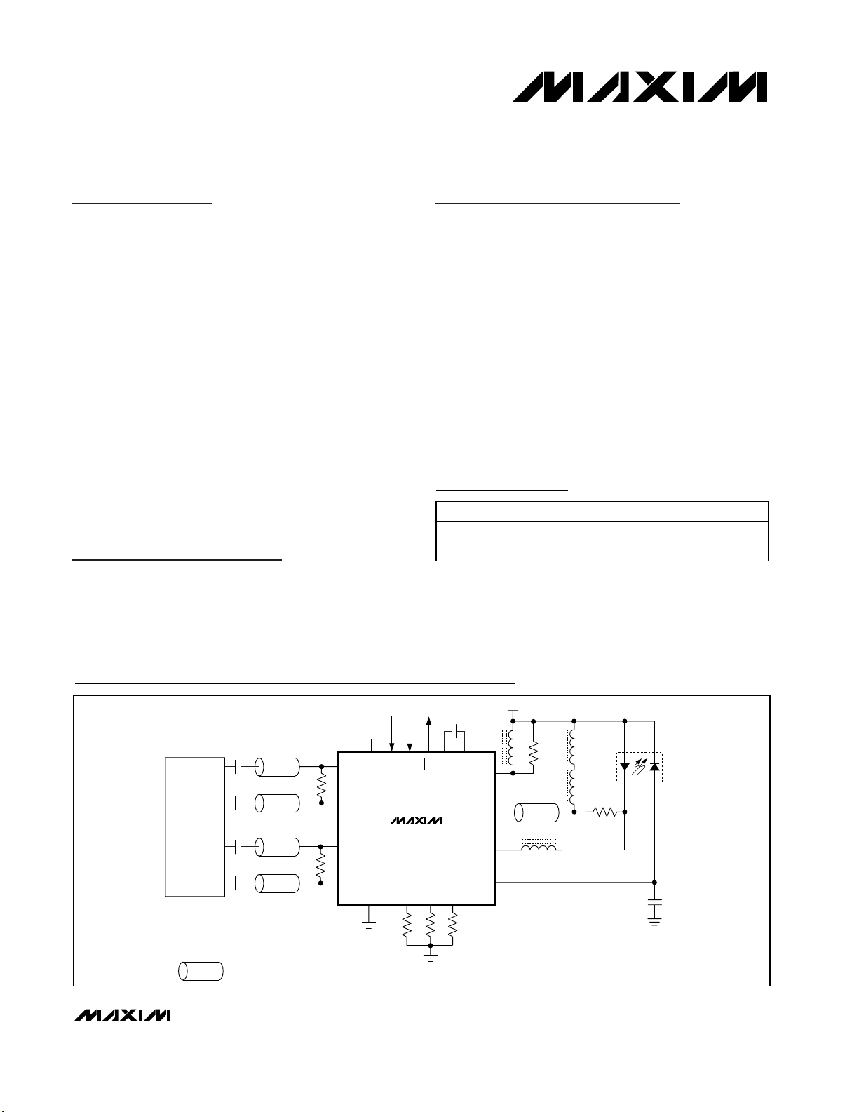
Typical Application Circuit
Pin Configuration appears at end of data sheet.
V
CC
CC
V
EN
GND
2.5Gbps
SERIALIZER
WITH CLOCK
GENERATION
DATA +
DATA -
CLK+
CLK-
50Ω
50Ω
50Ω
50Ω
DATA +
100Ω
DATA -
CLK+
100Ω
CLK-
PART TEMP RANGE PIN-PACKAGE
MAX3273EGG
MAX3273E/D -40°C to +85°C Dice**
V
LATCH
MAX3273
MODSET
FAIL
BIASMAX
0.01µF
APCFILT1
APCSET
APCFILT2
OUT-
OUT+
BIAS
MD
CC
L
P1
-40°C to +85°C 24 QFN-EP* (4mm × 4mm)
L
P1
25Ω
L
P2
25Ω
20Ω
0.056µF
500pF
REPRESENTS A CONTROLLED-IMPEDANCE TRANSMISSION LINE.
Page 2
MAX3273
+3.3V, 2.5Gbps Low-Power Laser Driver
2 _______________________________________________________________________________________
ABSOLUTE MAXIMUM RATINGS
DC ELECTRICAL CHARACTERISTICS
(VCC= +3.14V to +3.6V, TA= -40°C to +85°C. Typical values are at VCC= +3.3V, I
BIAS
= 60mA, I
MOD
= 30mA, TA= +25°C, unless
otherwise noted.) (Note 1)
Stresses beyond those listed under “Absolute Maximum Ratings” may cause permanent damage to the device. These are stress ratings only, and functional
operation of the device at these or any other conditions beyond those indicated in the operational sections of the specifications is not implied. Exposure to
absolute maximum rating conditions for extended periods may affect device reliability.
Supply Voltage, VCC..............................................-0.5V to +6.0V
Current into BIAS, OUT+, OUT- ......................-20mA to +150mA
Current into MD.....................................................-5mA to +5mA
Voltage at DATA+, DATA-, CLK+,
CLK-, LATCH, EN, FAIL..........................-0.5V to (V
CC
+ 0.5V)
Voltage at MODSET, BIASMAX,
APCSET, APCFILT1, APCFILT2.........................-0.5V to +3.0V
Voltage at BIAS .........................................+1.0V to (V
CC
+ 1.5V)
Voltage at OUT+, OUT-.............................+1.5V to (V
CC
+ 1.5V)
Current into FAIL ...............................................-10mA to +10mA
Continuous Power Dissipation (T
A
= +85°C)
24-Pin QFN (derate 274mW/°C above +85°C) ..........1781mW
Storage Temperature Range .............................-55°C to +150°C
Operating Junction Temperature ......................-55°C to +150°C
Die Attach Temperature (die) ..........................................+400°C
Lead Temperature (soldering, 10s) .................................+300°C
Supply Current I
Bias-Current Range I
Bias Off-Current EN = high (Note 2), V
Bias-Current Stability APC open loop (Note 3)
PARAMETER SYMBOL CONDITIONS MIN TYP MAX UNITS
CC
BIAS
Excluding I
Voltage on BIAS pin (V
BIAS
and I
MOD
) = VCC - 1.6V 1 100 mA
BIAS
≤ 2.6V 0.2 mA
BIAS
I
BIAS
I
BIAS
Bias-Current Absolute Accuracy APC open loop (Note 4) -15 +15 %
Differential Input Voltage V
Common-Mode Input Voltage V
TTL Input High Voltage V
TTL Input Low Voltage V
TTL Output High V
TTL Output Low V
ICM
Figure 1 0.2 1.6 V
ID
IH
IL
Sourcing 50µA 2.4 V
OH
Sinking 100µA 0.4 V
OL
MD Voltage 1.6 V
Monitor Diode DC-Current Range I
Monitor-Diode Bias Set Point
Stability
MD
(Note 3) 18 1000 µA
IMD = 1000µA -480 83 +480
I
= 18µA -480 159 +480
MD
Monitor-Diode Bias Absolute
Accuracy
= 100mA 61
= 1mA 198
30 45 mA
VCC -
1.49
VCC -
1.32
VCC V
ID
/4
2.0 V
0.8 V
-15 +15 %
ppm/°C
P-P
V
ppm/°C
Page 3
MAX3273
+3.3V, 2.5Gbps Low-Power Laser Driver
_______________________________________________________________________________________ 3
AC ELECTRICAL CHARACTERISTICS
(VCC= +3.14V to +3.6V, TA= -40°C to +85°C. Typical values are at VCC= +3.3V, I
BIAS
= 60mA, I
MOD
= 30mA, TA= +25°C, unless
otherwise noted.) (Notes 5, 6)
Note 1: Specifications at -40°C are guaranteed by design and characterization. Dice are tested at T
A
= +25°C only.
Note 2: Both the bias and modulation currents are switched off if any of the current set pins is grounded.
Note 3: Guaranteed by design and characterization.
Note 4: Accuracy refers to part-to-part variation.
Note 5: AC characterization was performed by using the circuit in Figure 2.
Note 6: AC characteristics are guaranteed by design and characterization, and measured using a 2.5Gbps 2
13
- 1 PRBS input data
pattern with 80 consecutive zeros and 80 consecutive ones added.
Note 7: Measured using a 2.5Gbps repeating 0000 1111 pattern.
Note 8: PWD = (wide pulse - narrow pulse) / 2.
Modulation-Current Range I
Modulation Off-Current EN = high 0.2 mA
Modulation-Current Stability
Modulation-Current Absolute
Accuracy
Output Current Rise Time t
Output Current Fall Time t
Output Overshoot/Undershoot δ (Note 7) 15 %
Enable and Startup Delay APC open loop 364 ns
Maximum Consecutive Identical
Digits
Pulse-Width Distortion PWD (Notes 7, 8) 3 45 ps
Random Jitter 1.0 1.5 ps
Input Latch Setup Time T
Input Latch Hold Time T
PARAMETER SYMBOL CONDITIONS MIN TYP MAX UNITS
MOD
(Note 3) 5 60 mA
I
= 60mA -480 64 +480
MOD
= 5mA -480 34 +480
I
MOD
(Note 4) -15 +15 %
20% to 80% (Note 7) 52 87 ps
R
20% to 80% (Note 7) 59 104 ps
F
LATCH = high (Figure 1) 75 150 ps
SU
LATCH = high (Figure 1) 0 50 ps
HD
ppm/°C
80 bits
RMS
Page 4
MAX3273
+3.3V, 2.5Gbps Low-Power Laser Driver
4 _______________________________________________________________________________________
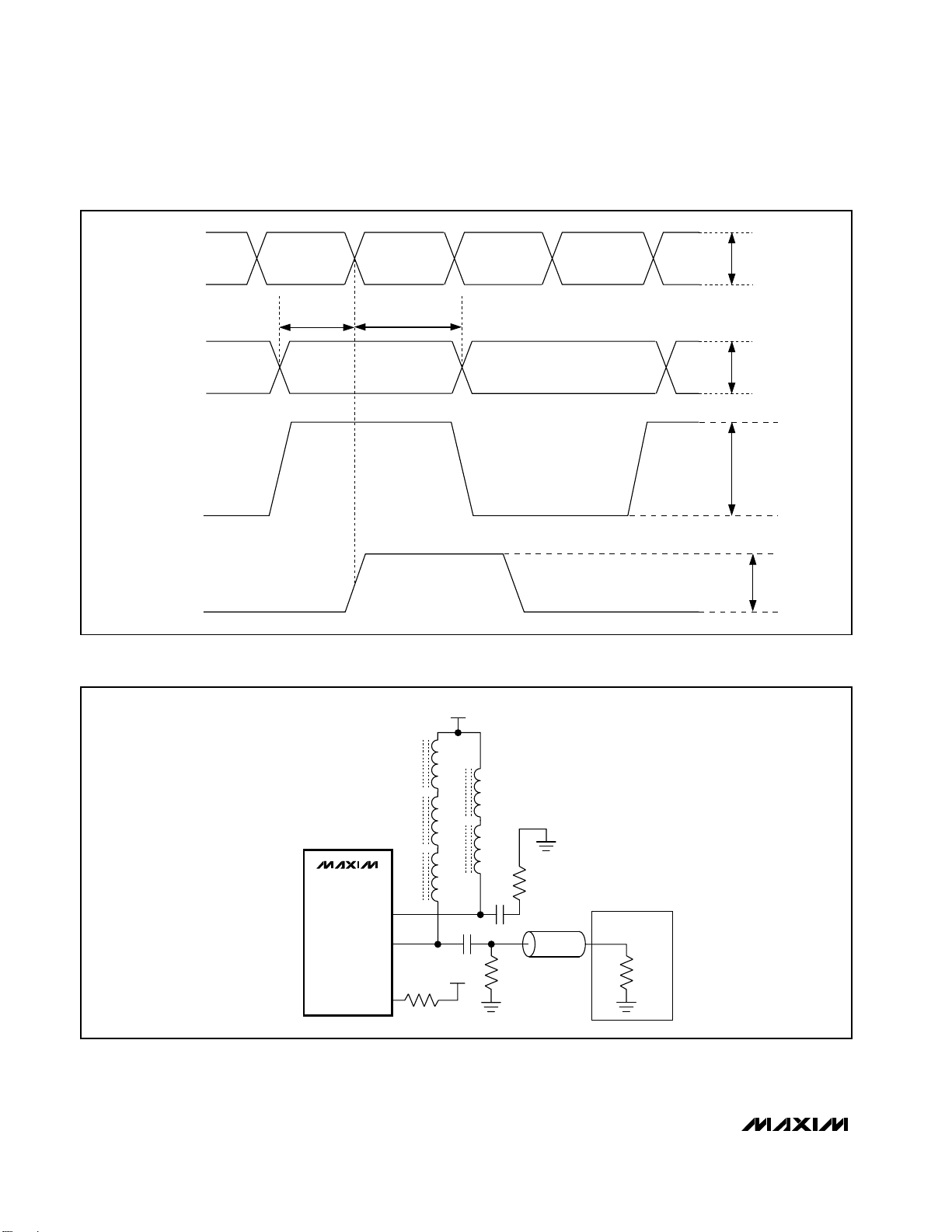
Figure 1. Required Input Signal and Setup/Hold-Time Definition
Figure 2. Output Termination for Characterization
CLK+
CLK-
VIS = 0.1V TO 0.8V
T
SU
DATA -
DATA +
(DATA+) - (DATA-)
I
MOD
= MURATA BLM11HA601SPT
L
P1
= MURATA BLM21HA102SPT
L
P2
= COILCRAFT D01607C-333
L
P3
T
HD
V
= 0.1V TO 0.8V
IS
V
= 0.2V TO 1.6V
ID
5mA TO 60mA
V
CC
L
P3
L
P2
L
P2
L
P1
L
OUT-
OUT+
BIAS
P1
15Ω
0.056µF
V
CC
0.056µF
50Ω
25Ω
OSCILLOSCOPE
50Ω
50Ω
MAX3273
Page 5
MAX3273
+3.3V, 2.5Gbps Low-Power Laser Driver
_______________________________________________________________________________________ 5
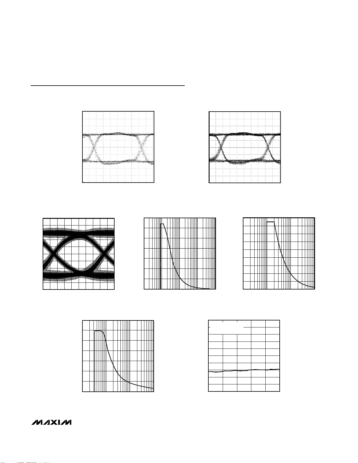
Typical Operating Characteristics
(V
CC
= 3.3V, TA = +25°C, unless otherwise noted.)
ELECTRICAL EYE DIAGRAM
(I
MOD
= 20mA, 213 - 1 80CID)
MAX3273 toc01
125mV/div
60ps/div
ELECTRICAL EYE DIAGRAM
(I
MOD
= 60mA, 213 - 1 80CID)
MAX3273 toc02
400mV/div
60ps/div
I
BIASMAX
vs. R
BIASMAX
MAX3273 toc04
R
BIASMAX
(kΩ)
I
BIASMAX
(mA)
140
0
20
40
60
80
120
100
0.1 10 1001 1000
57ps/div
MITSUBISHI ML725C8F
LASER DIODE
OPTICAL EYE DIAGRAM
(2.488Gbps, 1300nm FP LASER,
1.87GHz FILTER)
MAX3273 toc03
0
0.1 100101
I
MOD
vs. R
MODSET
30
10
70
50
90
40
20
80
60
MAX3273 toc05
R
MODSET
(kΩ)
I
MOD
(mA)
0.1 10 100
IMD vs. R
APCSET
MAX3273 toc06
R
APCSET
(kΩ)
I
MD
(mA)
1
1.4
0
0.2
0.4
0.6
0.8
1.2
1.0
0
30
20
10
40
50
60
70
80
90
100
-40 10-15 35 60 85
SUPPLY CURRENT vs. TEMPERATURE
MAX3273 toc07
TEMPERATURE (°C)
SUPPLY CURRENT (mA)
EXCLUDE I
BIAS
, I
MOD
25Ω LOAD
Page 6

MAX3273
+3.3V, 2.5Gbps Low-Power Laser Driver
6 _______________________________________________________________________________________
Typical Operating Characteristics (continued)
(V
CC
= 3.3V, TA = +25°C, unless otherwise noted.)
25
20
15
10
5
PWD (ps)
0
-5
-10
-15
52515 35 45 55 65
PULSE-WIDTH DISTORTION vs. I
I
(mA)
MOD
MOD
MAX3273 toc08
TYPICAL DISTRIBUTION OF I
50
40
30
20
PERCENT OF UNITS (%)
10
0
49.0
52.050.5 53.5 55.0 56.5 58.0 59.5
RISE TIME (ps)
RISE TIME
MOD
I
= 60mA
MOD
MEAN = 52.27ps
STDEV = 1.57ps
MAX3273 toc09
TYPICAL DISTRIBUTION OF I
40
30
20
PERCENT OF UNITS (%)
10
0
60 6261 63 64 65 66 67
FALL TIME (ps)
FALL TIME
MOD
I
= 5mA
MOD
MEAN = 63.23ps
STDEV = 1.21ps
TYPICAL DISTRIBUTION OF I
40
30
20
PERCENT OF UNITS (%)
10
MAX3273 toc10
PERCENT OF UNITS (%)
RISE TIME
MOD
I
= 5mA
MOD
MEAN = 48.57ps
STDEV = 1.48ps
TYPICAL DISTRIBUTION OF I
60
I
MOD
50
40
30
20
10
0
57 60 6158 59 62 63 64
FALL TIME (ps)
MAX3273 toc12
MEAN = 59.41ps
STDEV = 1.33ps
FALL TIME
MOD
= 60mA
MAX3273 toc11
0
45 4746 48 49 50 51 52 53
RISE TIME (ps)
Page 7

MAX3273
+3.3V, 2.5Gbps Low-Power Laser Driver
_______________________________________________________________________________________ 7
Pin Description
PIN NAME FUNCTION
1, 4, 13, 15, 18 V
2 DATA+ Noninverting Data Input, with On-Chip Biasing
3 DATA- Inverting Data Input, with On-Chip Biasing
5 CLK+ Noninverting Clock Input for Data Retiming, with On-Chip Biasing
6 CLK- Inverting Clock Input for Data Retiming, with On-Chip Biasing
7, 9, 12 GND Ground
8 LATCH Data Retiming Enable Input, Active-High. Retiming disabled when floating or pulled low.
10 EN
11 MODSET A resistor connected from this pin to ground sets the desired modulation current.
14 BIAS Laser Bias Current Output. Connect to the laser through an inductor.
16 OUT+ Positive Modulation-Current Output. I
17 OUT-
19 MD
20 APCFILT1
21 APCFILT2 See above.
22 FAIL TTL/CMOS Failure Output, Active-Low. Indicates APC failure when low.
23 APCSET
24 BIASMAX
CC
Power-Supply Voltage
TTL/CMOS Enable Input. Low for normal operation. Float or pull high to disable laser bias and
modulation currents. Internal 100kΩ pullup to V
flows into this pin when input data is high.
MOD
Negative Modulation-Current Output. Current flows into this pin when input data is low. Connect
to load equivalent to that on OUT+ to maintain differential output balance.
Monitor Diode Input. Connect this pin to the anode of the monitor diode. Leave floating for
open-loop operation.
A capacitor between APCFILT1 and APCFILT2 sets the dominant pole of the APC feedback
loop (C
A resistor connected from this pin to ground sets the desired average optical power. Connect a
100kΩ resistor to GND for open-loop operation.
A resistor connected from this pin to ground sets the maximum bias current. The APC function
can subtract current from this maximum value, but cannot add to it. For open-loop operation,
this pin sets the laser bias current.
= 0.01µF). Ground APCFILT1 for open-loop operation.
APCFILT
CC
.
EP
EXPOSED
PAD
Ground. Solder this pad to ground.
Page 8

MAX3273
+3.3V, 2.5Gbps Low-Power Laser Driver
8 _______________________________________________________________________________________
Detailed Description
The MAX3273 laser driver consists of two main parts: a
high-speed modulation driver and a laser-biasing block
with automatic power control (APC). The circuit design
is optimized for both high-speed and low-voltage
(+3.3V) operation. To minimize the jitter of the input signal at speeds as high as 2.7Gbps, the device accepts
a differential CML clock signal for data retiming. When
LATCH is high, the input data is synchronized by the
clock signal. When LATCH is low, the input data is
directly applied to the output stage.
The output stage is composed of a high-speed differential pair and a programmable modulation current
source. Because the modulation output drives a maximum current of 60mA into the laser with an edge speed
of 59ps, large transient voltage spikes can be generated (due to the parasitic inductance of the laser). These
transients and the laser-forward voltage leave insuffi-
cient headroom for the proper operation of the laser driver if the modulation output is DC-coupled to the laser
diode. To solve this problem, the MAX3273’s modulation output is AC-coupled to the cathode of a laser
diode. An external pullup inductor is necessary to DCbias the modulation output at V
CC
. Such a configuration
isolates laser-forward voltage from the output circuitry
and the supply voltage VCC. A simplified functional diagram is shown in Figure 3.
The MAX3273 modulation output is optimized for driving a 25Ω load. Modulation current swings of 75mA
are possible, but because of minimum power-supply
and jitter requirements at 2.5Gbps, the specified maximum modulation current is limited to 60mA. To interface with the laser diode, a damping resistor (RD) is
required for impedance matching. An RC-shunt network might also be necessary to compensate for the
laser-diode parasitic inductance, thereby improving the
Figure 3. Functional Diagram
DATA
CLK
EN
MODSET BIASMAX APCFILT1 APCFILT2 APCSET
R
MODSET
D
MAX3273
x160
V
BG
Q
R
BIASMAX
LATCH
0
MUX
1
V
CC
L
P1
OUT-
OUT+
I
MOD
V
CC
FAILURE
DETECTOR
TIA
I
APCSET
x190
C
APCFILT
L
P1
L
P2
BIAS
MD
R
APCSET
FAIL
25Ω
C
D
R
V
CC
I
MD
V
CC
D
I
BIAS
500pF
Page 9

MAX3273
+3.3V, 2.5Gbps Low-Power Laser Driver
_______________________________________________________________________________________ 9
optical output ringing and duty-cycle distortion. Refer to
Maxim application note HFAN 02.0, Interfacing Maxim
Laser Drivers with Laser Diodes, for more information.
At the data rate of 2.5Gbps, any capacitive load at the
cathode of a laser diode degrades the optical output
performance. Because the BIAS output is directly connected to the laser cathode, the parasitic capacitance
associated with this pin is minimized by using an inductor to isolate the BIAS pin from the laser cathode.
Automatic Power Control (APC)
To maintain constant average optical power, the
MAX3273 incorporates an APC loop to compensate for
the changes in laser threshold current over temperature
and lifetime. A back-facet photodiode mounted in the
laser package is used to convert the optical power into
a photocurrent. The APC loop adjusts the laser bias
current so that the monitor current is matched to a reference current set by R
APCSET
. The time constant of
the APC loop is determined by an external capacitor
(C
APCFILT
). To minimize the pattern-dependent jitter
associated with the APC loop-time constant, and to
guarantee loop stability, the recommended value for
C
APCFILT
is 0.01µF.
When the APC loop is functioning, the maximum allowable bias current is set by an external resistor, R
BIASMAX
.
An APC failure flag (FAIL) is asserted low when the bias
current can no longer be adjusted to achieve the desired
average optical power.
APC closed-loop operation requires the user to set three
currents with external resistors connected between
ground and BIASMAX, MODSET, and APCSET (see
Figure 3). Detailed guidelines for these resistor settings
are described in the Design Procedure section.
Open-Loop Operation
If necessary, the MAX3273 is fully operational without
APC. To disable the APC loop, ground the APCFILT1
pin. In this case, the laser current is directly set by two
external resistors connected from ground to BIASMAX
and MODSET. See the Design Procedure section for
more details on open-loop operation.
Optional Data Input Latch
To minimize jitter in the input data, connect a synchronous differential clock signal to the CLK+ and CLKinputs. When the LATCH control input is tied high, the
input data is retimed on the rising edge of CLK+. If
LATCH is tied low or left floating, the retiming function is
disabled and the input data is directly connected to the
output stage. When this latch function is not used, connect CLK+ to V
CC
and leave CLK- unconnected.
Output Enable
The MAX3273 incorporates a TTL/CMOS input to
enable the output. When EN is low, the modulation and
bias outputs are enabled. When EN is high or floating,
both the bias and modulation currents are off. The typical enable time is 364ns, and the typical disable time is
27ns when the bias is operated open loop.
Slow-Start
For laser safety reasons, the MAX3273 incorporates a
slow-start circuit that provides a delay of 364ns for
enabling a laser diode.
APC Failure Monitor
The MAX3273 provides an APC failure monitor
(TTL/CMOS) to indicate an APC loop tracking failure.
FAIL is asserted low when the APC loop no longer can
regulate the bias current to maintain the desired monitor diode current. FAIL asserts low when the APC loop
is disabled.
Short-Circuit Protection
The MAX3273 provides short-circuit protection for the
modulation and bias current sources. If BIASMAX,
MODSET, or APCSET is shorted to ground, the bias
and modulation output turns off.
Design Procedure
When designing a laser transmitter, the optical output
usually is expressed in terms of average power and
extinction ratio. Table 1 gives relationships helpful in
converting between the optical average power and the
modulation current. These relationships are valid if the
mark density and duty cycle of the optical waveform
are 50%.
Programming the Modulation Current
For a given laser power (P
AVG
), slope efficiency (η), and
extinction ration (re), the modulation current can be calculated using Table 1. See the I
MOD
vs. R
MODSET
graph in the Typical Operating Characteristics and
select the value of R
MODSET
that corresponds to the
required current at +25°C. The equation below provides
a derivation of the modulation current using Table 1.
I
=× ×
2
MOD
Pr
AVE e
−
1
r
+
1η
e
Page 10

MAX3273
+3.3V, 2.5Gbps Low-Power Laser Driver
10 ______________________________________________________________________________________
Programming the Bias Current
with APC Disabled
When using the MAX3273 in open-loop operation, the
bias current is determined by the R
BIASMAX
resistor. To
select this resistor, see the I
BIASMAX
vs. R
BIASMAX
graph
in the Typical Operating Characteristics and select the
value of R
BIASMAX
that corresponds to the required
I
BIASMAX
at +25°C. Ground the APCFILT1 pin for open-
loop operation.
Programming the Bias Current
with APC Enabled
When the MAX3273’s APC feature is used, program the
average optical power by adjusting the APCSET resistor. To select this resistor, determine the desired monitor current to be maintained over temperature and life.
See the IMDvs. R
APCSET
graph in the Typical
Operating Characteristics and select the value of R
APC-
SET
that corresponds to the required current.
When using the MAX3273 in closed-loop operation, the
R
BIASMAX
resistor sets the maximum bias current available to the laser diode over temperature and life. The
APC loop can subtract from this maximum value but
cannot add to it. See the I
BIASMAX
vs. R
BIASMAX
graph
in the Typical Operating Characteristics and select the
value of R
BIASMAX
that corresponds to the end-of-life
bias current at +85°C.
Interfacing with Laser Diodes
To minimize optical output aberrations caused by signal reflections at the electrical interface to the laser
diode, a series-damping resistor (RD) is required (see
the Typical Application Circuit). Additionally, the
MAX3273 outputs are optimized for a 25Ω load.
Therefore, the series combination of RDand RL(where
RLrepresents the laser-diode resistance) should equal
25Ω. Typical values for RD are 18Ω to 23Ω. For best
performance, a bypass capacitor (0.01µF typical)
should be placed as close as possible to the anode of
the laser diode. Depending on the exact characteristics
of the laser diode and PC board layout, a resistor (RP)
of 50Ω to 100Ω in parallel with pullup inductor LP1can
be useful in damping overshoot and ringing in the optical output.
In some applications (depending on laser-diode parasitic inductance), an RC-shunt network between the
laser cathode and ground helps minimize optical output aberrations. Starting values for most coaxial lasers
are R = 75Ω in series with C = 3.3pF. These values
should be experimentally adjusted until the optical output waveform is optimized.
Pattern-Dependent Jitter
When transmitting NRZ data with long strings of consecutive identical digits (CIDs), LF droop can occur
and contribute to pattern-dependent jitter (PDJ). To
minimize this PDJ, three external components must be
properly chosen: capacitor (C
APCFILT
), which dominates the APC loop time constant; pullup inductor (LP);
and AC-coupling capacitor (CD).
To filter out noise effects and guarantee loop stability,
the recommended value for C
APCFILT
is 0.01µF. This
results in an APC loop bandwidth of 100kHz or a time
constant of 15µs. As a result, the PDJ associated with
an APC loop time constant can be ignored.
The time constant associated with the output pullup
inductor (LP≈ LP2) and the AC-coupling capacitor (CD)
affects the PDJ. For such a second-order network, the
PDJ is dominated by LPbecause of the low frequency
cutoff. For a data rate of 2.5Gbps, the recommended
value for CDis 0.056µF. During the maximum CID period, limit the peak voltage droop to less than 12% of the
average (6% of the amplitude). The time constant can
be estimated by:
If τLP= LP / 25Ω, and t = 100UI ≈ 40ns, then LP=
7.8µH. To reduce the physical size of this element (LP),
use of SMD ferrite beads is recommended (Figure 2).
To achieve even greater immunity to droop, use an
optional third inductor (33µH, LP3in Figure 2).
Input Termination Requirement
The MAX3273 data and clock inputs are CML compatible. However, it is not necessary to drive the IC with a
standard CML signal. As long as the specified differential voltage swings are met, the MAX3273 operates
properly.
Calculating Power Consumption
The junction temperature of the MAX3273 dice must be
kept below +150°C at all times. The total power dissipation of the MAX3273 can be estimated by the following:
P = VCC× ICC+ (VCC- Vf) ✕I
BIAS
+ I
MOD
✕
(VCC- 25 ✕I
MOD
/ 2)
where I
BIAS
is the maximum bias current set by
R
BIASMAX
, I
MOD
is the modulation current, and Vfis the
typical laser forward voltage.
Junction temperature = P(W) ✕37 (°C/W)
12 1
78%.==
−
−
e
t
t
LP
LP
τ
τ
Page 11

MAX3273
+3.3V, 2.5Gbps Low-Power Laser Driver
______________________________________________________________________________________ 11
Applications Information
An example of how to set up the MAX3273 follows.
Select Laser
A communication-grade laser should be selected for
2.5Gbps/2.7Gbps applications. Assume the laser output average power is P
AVG
= 0, the minimum extinction
ratio is re= 6.6 (8.2dB), the operating temperature is
-40°C to +85°C, and the laser diode has the following
characteristics:
• Wavelength: λ = 1310nm
• Threshold Current: I
TH
= 22mA at +25°C
• Threshold Temperature Coefficient: β
TH
= 1.3%/°C
• Laser-to-Monitor Transfer: ρ
MON
= 0.2A/W
• Laser Slope Efficiency: η = 0.05mW/mA at +25°C
Determine R
APCSET
The desired monitor diode current is estimated by I
MD
= P
AVG×ρMON
= 200µA. The IMDvs. R
APCSET
graph
in the Typical Operating Characteristics shows that
R
APCSET
should be 7.5kΩ.
Determine R
MODSET
To achieve a minimum extinction ratio (re) of 6.6 over
temperature and lifetime, calculate the required extinction ratio at +25°C. Assuming re= 20, the peak-to-peak
optical power P
P-P
= 1.81mW, according to Table 1.
The required modulation current is 1.81mW/
(0.05mW/mA) = 36.2mA. The I
MOD
vs. R
MODSET
graph
in the Typical Operating Characteristics shows that
R
MODSET
should be 5kΩ.
Determine R
BIASMAX
Calculate the maximum threshold current (I
TH(MAX)
) at
TA= +85°C and end of life. Assuming I
TH(MAX)
=
50mA, the maximum bias current should be: I
BIASMAX
= I
TH(MAX)
+ (I
MOD
/ 2). In this example, I
BIASMAX
=
68.1mA. The I
BIASMAX
vs. R
BIASMAX
graph in the
Typical Operating Characteristics shows that R
BIASMAX
should be 3.5kΩ.
Note: Assuming a 50% average input duty cycle and mark density.
Table 1. Optical Power Relations
PARAMETER SYMBOL RELATION
Average Power P
Extinction Ratio r
Optical Power of a 1 P
Optical Power of a 0 P
Optical Amplitude P
Laser Slope Efficiency ηη = P
Modulation Current I
Threshold Current I
Bias Current I
Laser-to-Monitor Transfer ρ
AVG
e
1
0
P-P
MOD
TH
BIAS
MON
P
P-P
P
AVG
P1 = 2P
P0 = 2P
= P1 - P0 = 2P
I
BIAS
= (P0 + P1) / 2
re = P1 / P
/ (re + 1)
AVGre
/ (re + 1)
AVG
AVG(re
/ I
P-P
I
= P
MOD
P-P
P0 at 1 ≥ I
≥ ITH + I
I
/ P
MD
AVG
0
- 1) / (re + 1)
MOD
/ η
TH
/ 2
MOD
Page 12

MAX3273
+3.3V, 2.5Gbps Low-Power Laser Driver
12 ______________________________________________________________________________________
Interface Models
Figures 4 and 5 show simplified input and output circuits for the MAX3273 laser driver. If dice are used,
replace package parasitic elements with bondwire parasitic elements.
Wire-Bonding Die
For high-current density and reliable operation, the
MAX3273 uses gold metalization. Make connections to
the die with gold wire only, using ball-bonding techniques. Wedge bonding is not recommended. Die-pad
size is 4 mils (100µm) square, and die thickness is 14
mils (350µm).
Layout Considerations
To minimize inductance, keep the connections between
the MAX3273 output pins and laser diode as close as
possible. Optimize the laser-diode performance by
placing a bypass capacitor as close as possible to the
laser anode. Use good high-frequency layout techniques and multilayer boards with uninterrupted ground
planes to minimize EMI and crosstalk.
Laser Safety and IEC 825
Using the MAX3273 laser driver alone does not ensure
that a transmitter design is compliant with IEC 825. The
entire transmitter circuit and component selections
must be considered. Customers must determine the
level of fault tolerance required by their application,
recognizing that Maxim products are not designed or
authorized for use as components in systems intended
for surgical implant into the body, for applications
intended to support or sustain life, or for any other
application where the failure of a Maxim product could
create a situation where personal injury or death may
occur.
Chip Information
TRANSISTOR COUNT: 1672
PROCESS: SiGe
ISOLATED SUBSTRATE
Page 13

MAX3273
+3.3V, 2.5Gbps Low-Power Laser Driver
______________________________________________________________________________________ 13
Figure 4. Simplified Input Circuit
Figure 5. Simplified Output Circuit
Chip Topography
24
23
22
21
20
19
BIASMAX
APCSET
FAIL
APCFILT2
APCFILT1
MD
7
8
9
10
11
12
GND
LATCH
GND
EN
MODSET
GND
13
14
15
16
17
18
V
CC
*EXPOSED PAD IS CONNECTED TO GND.
BIAS
V
CC
OUT+
OUT-
V
CC
6
5
4
3
2
1
CLK-
CLK+
V
CC
DATA-
DATA+
V
CC
MAX3273
QFN*
TOP VIEW
Pin Configuration
V
V
CC
CC
PACKAGE
0.9nH
+
IN
0.1pF
IN-
0.9nH
0.1pF
V
CC
V
CC
16kΩ
5kΩ
5kΩ
24kΩ
MD
APCFILT1
APCFILT2
GND
FAIL
APCSET
N.C.
BIASMAX
GND
N.C.
CC
V
OUT-
OUT+
PACKAGE
0.9nH
0.1pF
0.9nH
0.1pF
OUT+
OUT-
CC
V
BIAS
CC
V
GND
GND
GND
MODSET
N.C.
EN
79 mil
(2.01mm)
N.C.
GND
LATCH
GND
CC
V
DATA+
DATA-
CC
64 mil
(1.63mm)
VCCV
CLK+
CLK-
N.C.
Page 14

MAX3273
+3.3V, 2.5Gbps Low-Power Laser Driver
14 ______________________________________________________________________________________
Package Information
(The package drawing(s) in this data sheet may not reflect the most current specifications. For the latest package outline information
go to www.maxim-ic.com/packages
.)
12,16,20, 24L QFN.EPS
Page 15

MAX3273
+3.3V, 2.5Gbps Low-Power Laser Driver
Maxim cannot assume responsibility for use of any circuitry other than circuitry entirely embodied in a Maxim product. No circuit patent licenses are
implied. Maxim reserves the right to change the circuitry and specifications without notice at any time.
Maxim Integrated Products, 120 San Gabriel Drive, Sunnyvale, CA 94086 408-737-7600 ____________________ 15
© 2002 Maxim Integrated Products Printed USA is a registered trademark of Maxim Integrated Products.
Package Information (continued)
(The package drawing(s) in this data sheet may not reflect the most current specifications. For the latest package outline information
go to www.maxim-ic.com/packages
.)
 Loading...