

Page 1
现货库存、技术资料、百科信息、热点资讯,精彩尽在鼎好!
General Description
The MAX3272/MAX3272A 2.5Gbps limiting amplifiers
accept a wide range of input voltages and provide a
constant-level output voltage with controlled edge
speeds. Additional features include power detectors
with programmable loss-of-signal (LOS) indication, an
optional squelch function that mutes the data output signal when the input voltage falls below a programmable
threshold, and an output polarity selector. These parts
exhibit excellent jitter performance and have low power
dissipation.
The MAX3272/MAX3272A feature current-mode logic
(CML) data outputs that are tolerant of inductive connectors, and are available in a 4mm ✕ 4mm QFN package or in die form (MAX3272 only). Along with the
MAX3271, the MAX3272/MAX3272A are ideal for lowpower, compact optical receivers.
Applications
Gigabit Ethernet Optical Receivers
Fibre Channel Optical Receivers
System Interconnects
2.5Gbps Optical Receivers
SONET/SDH Receivers
Features
♦ Single +3.3V Power Supply
♦ 33mA Supply Current
♦ 5ps Deterministic Jitter
♦ 90ps Edge Speed
♦ Output Squelch Function
♦ Programmable Loss-of-Signal Function
♦ CML Output Interface
♦ 20-Pin 4mm ✕ 4mm QFN or Thin QFN Package
♦ Selectable Output Polarity
MAX3272/MAX3272A
+3.3V, 2.5Gbps Low-Power
Limiting Amplifiers
________________________________________________________________ Maxim Integrated Products 1
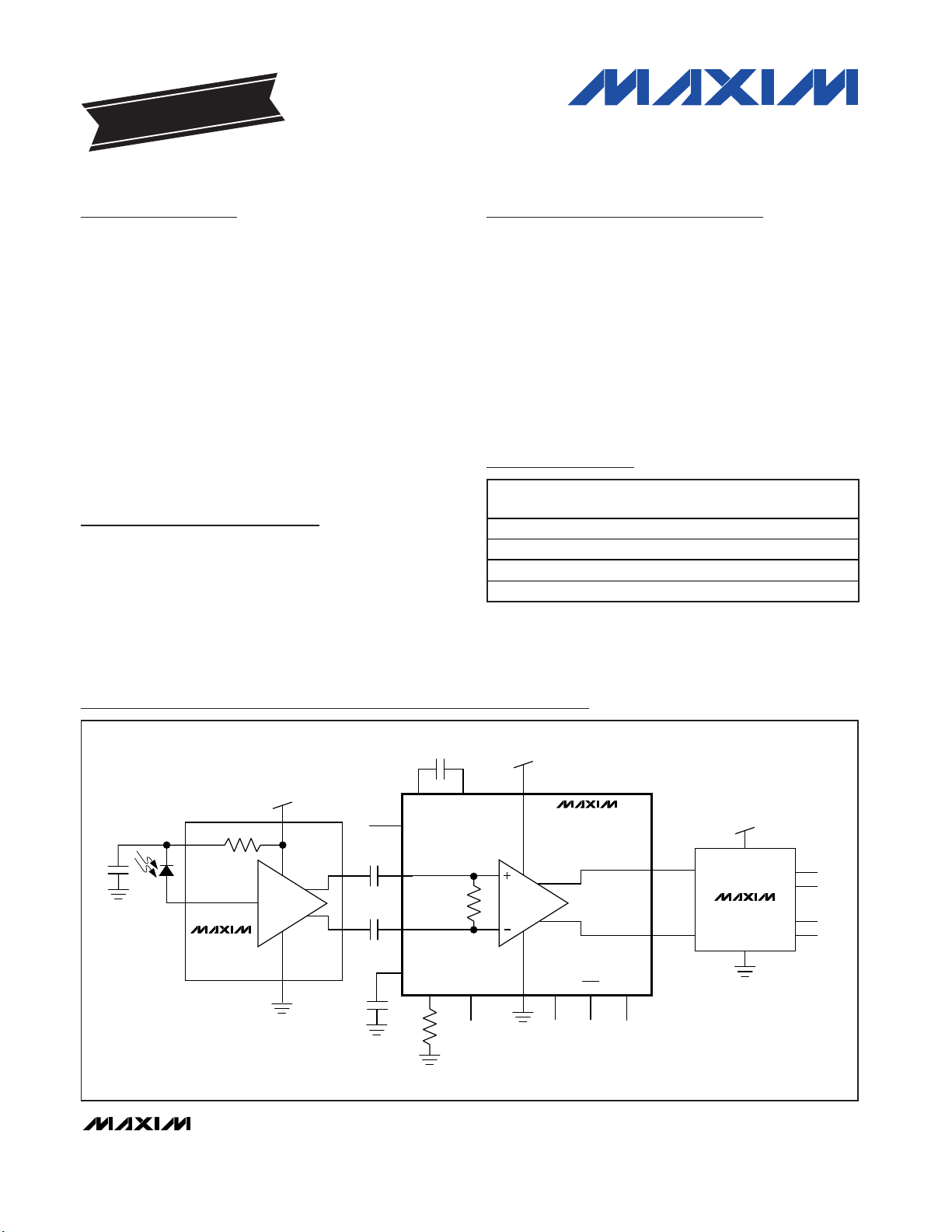
Ordering Information
+3.3V
+3.3V
+3.3V
C
AZ
CAZ1
OUTPOL
CAZ2 V
CC
0.1µF
0.1µF
TH SQUELCH
C
CLOS
CLOS
100Ω
IN-
IN+
OUT+
SDI+ SDO+
V
CC
SDO-
SCLKO-
SCLKO+
SDI-
GND
CDR
OUT-
MAX3271
MAX3272/
MAX3272A
MAX3873
LOSGND
LOSS
OF
SIGNAL
LOS
R
TH
LEVEL
Typical Operating Circuit
19-2269; Rev 3; 11/04
For pricing, delivery, and ordering information, please contact Maxim/Dallas Direct! at
1-888-629-4642, or visit Maxim’s website at www.maxim-ic.com.
Pin Configuration appears at end of data sheet.
Typical Operating Circuits continue at end of data sheet.
PART
TEMP RANGE
PIN-
PACKAGE
CODE
MAX3272EGP
20 QFN G2044-3
MAX3272E/D
Dice* —
MAX3272AETP+
T2044-3
MAX3272AEGP
20 QFN G2044-3
+ Denotes Lead-Free Package.
*Dice are designed and guaranteed to operate from -40°C to
+85°C, but are tested only at T
A
= +25°C.
EVALUATION KIT
AVAILABLE
PACKAGE
-40°C to +85°C
-40°C to +85°C
-40°C to +85°C 20 Thin QFN
-40°C to +85°C
Page 2

MAX3272/MAX3272A
+3.3V, 2.5Gbps Low-Power
Limiting Amplifiers
2 _______________________________________________________________________________________
ELECTRICAL CHARACTERISTICS
(VCC= +3.0V to +3.6V, TA= -40°C to +85°C. Typical values are at VCC= +3.3V and TA= +25°C, unless otherwise noted.) (Note 1)
Stresses beyond those listed under “Absolute Maximum Ratings” may cause permanent damage to the device. These are stress ratings only, and functional
operation of the device at these or any other conditions beyond those indicated in the operational sections of the specifications is not implied. Exposure to
absolute maximum rating conditions for extended periods may affect device reliability.
Power-Supply Voltage (VCC).................................-0.5V to +6.0V
Voltage at IN+, IN- ..........................(V
CC
- 2.4V) to (VCC+ 0.5V)
Voltage at SQUELCH, CAZ1, CAZ2,
TH, CLOS ...............................................-0.5V to (V
CC
+ 0.5V)
Voltage at LOS,
LOS (MAX3272)...........................-0.5V to +6.0V
Voltage at LOS, LOS (MAX3272A) .............-0.5V to (V
CC
+ 0.5V)
Voltage at LEVEL...................................................-0.5V to +2.0V
Voltage at OUTPOL ...............................................-0.5V to +6.0V
Current into LOS, LOS ..........................................-1mA to +9mA
Differential Input Voltage (IN+ - IN-).................................2.5V
P-P
Continuous Current at IN+, IN- ...........................................50mA
Continuous Current at
CML Outputs (OUT+, OUT-) .........................-25mA to +25mA
Continuous Power Dissipation at +85°C
20-Pin Thin QFN (derate 16.9mW/°C above +85°C) ......1.1W
20-Pin QFN (derate 20mW/°C above +85°C) .................1.3W
Storage Ambient Temperature
Range (T
STG
).................................................-55°C to +150°C
Operating Junction Temperature
Range (T
J
) .....................................................-55°C to +150°C
Die Attach Temperature...................................................+400°C
Lead Temperature (soldering, 10s) .................................+300°C
PARAMETER
SYMBOL
CONDITIONS
MIN
TYP
MAX
UNITS
Supply Current I
CC
(Note 2) 33 44 mA
Input Data Rate 2.5
Gbps
Input Voltage Range V
IN
Differential 15
mV
P-P
Output Deterministic Jitter (Notes 3, 4, 5) 5 27
ps
P-P
Random Jitter (Notes 4, 6) 3
ps
RMS
15mV
P-P
< VIN ≤ 30mV
P-P
90
Data Output Edge Speed
(20% to 80%)
(Notes 3, 4)
90
ps
Differential Input Resistance R
IN
IN+ to IN- 95
Ω
Input-Referred Noise
µV
RMS
CML Output Voltage V
OUT
LEVEL open, R
LOAD
= 50Ω
mV
P-P
Output Signal when Squelched Outputs AC-coupled 2.2
mV
P-P
Power-Supply Noise Rejection PSNR f ≤ 2MHz (Note 7) 30 dB
CAZ = open 0.9
MHz
Low Frequency Cutoff f
OC
CAZ = 0.1µF 1.5 kHz
Output Resistance R
OUT
Single ended to V
CC
50
Ω
≤ 2.5GHz 10
Single-Ended Output Return
Loss
2.5GHz to 4.0GHz 9
dB
Differential Input Return Loss 4.0GHz 10 dB
V
IL
0.8
OUTPOL Input Limits
V
IH
2.4
V
LOS Hysteresis (Notes 3, 4, 8) 2 3.3 dB
C
CLOS
= open (Notes 3, 9, 10) 1
LOS Assert/Deassert Time
C
CLOS
= 0.01µF (Notes 3, 9, 10) 2.3 50
µs
Low LOS Assert Level RTH = 20kΩ (Notes 3, 10) 4.5 6.5
mV
P-P
Low LOS Deassert Level RTH = 20kΩ (Notes 3, 10) 9.5
mV
P-P
Medium LOS Assert Level RTH = 1kΩ (Notes 3, 10) 7.8
mV
P-P
Medium LOS Deassert Level RTH = 1kΩ (Notes 3, 10)
mV
P-P
High LOS Assert Level RTH = 80Ω (Notes 3, 10)
48
mV
P-P
ABSOLUTE MAXIMUM RATINGS
30mV
≤ VIN ≤ 1200mV
P-P
P-P
550 750 1200
42.5
24.3
100 105
220
12.9
17.4 22.4
1200
130
115
57.5
100
12.7
Page 3
MAX3272/MAX3272A
+3.3V, 2.5Gbps Low-Power
Limiting Amplifiers
_______________________________________________________________________________________ 3
ELECTRICAL CHARACTERISTICS (continued)
(VCC= +3.0V to +3.6V, TA= -40°C to +85°C. Typical values are at VCC= +3.3V and TA= +25°C, unless otherwise noted.)
PARAMETER
SYMBOL
CONDITIONS
MIN
TYP
MAX
UNITS
High LOS Deassert Level RTH = 80Ω (Notes 3, 10) 73
mV
P-P
LOS Output High Voltage Sinking 30µA 2.4 V
LOS Output Low Voltage Sourcing 1.2mA 0.4 V
Squelch Input Current
µA
Note 1: Dice are designed and guaranteed from -40°C to +85°C but are tested only at TA= +25°C.
Note 2: Supply current measurement excludes the current of the CML output stage (16mA typical). See Figure 1, Power-Supply
Current Measurement.
Note 3: Guaranteed by design and characterization.
Note 4: Input edge speed is controlled using 4-pole, lowpass Bessel filters with bandwidth approximately 75% of the maximum
data rate.
Note 5: Deterministic jitter is measured with a K28.5 pattern (0011 1110 1011 0000 0101). Deterministic jitter is the peak-to-peak
deviation from ideal time crossings, measured at the zero-level crossings of the differential output per ANSI X3.230, Annex A.
Note 6: Random jitter is measured with the minimum input signal. For Fibre Channel and Gigabit Ethernet applications, the peak-
to-peak random jitter is 14.1 times the RMS random jitter.
Note 7: Power-supply noise rejection (PSNR) is calculated by the equation PSNR = 20log (∆V
CC
/(∆V
OUT
)), where ∆V
OUT
is the
change in differential output voltage due to the power-supply noise, ∆V
CC
. See Power-Supply Noise Rejection vs.
Frequency in the Typical Operating Characteristics.
Note 8: Hysteresis is defined as: 20
✕ log(V
LOS-DEASSERT/VLOS-ASSERT
).
Note 9: Response time to a 10dB change in input power. For the specification guaranteed, the power is assumed to switch back
and forth between two levels (separated by 10dB and equidistant from assert and deassert levels) outside of the two
hysteresis thresholds.
Note 10: All power-detect AC parameters are guaranteed with a 2
23
- 1 PRBS, 2.5Gbps input, with the longest possible run of 80CID.
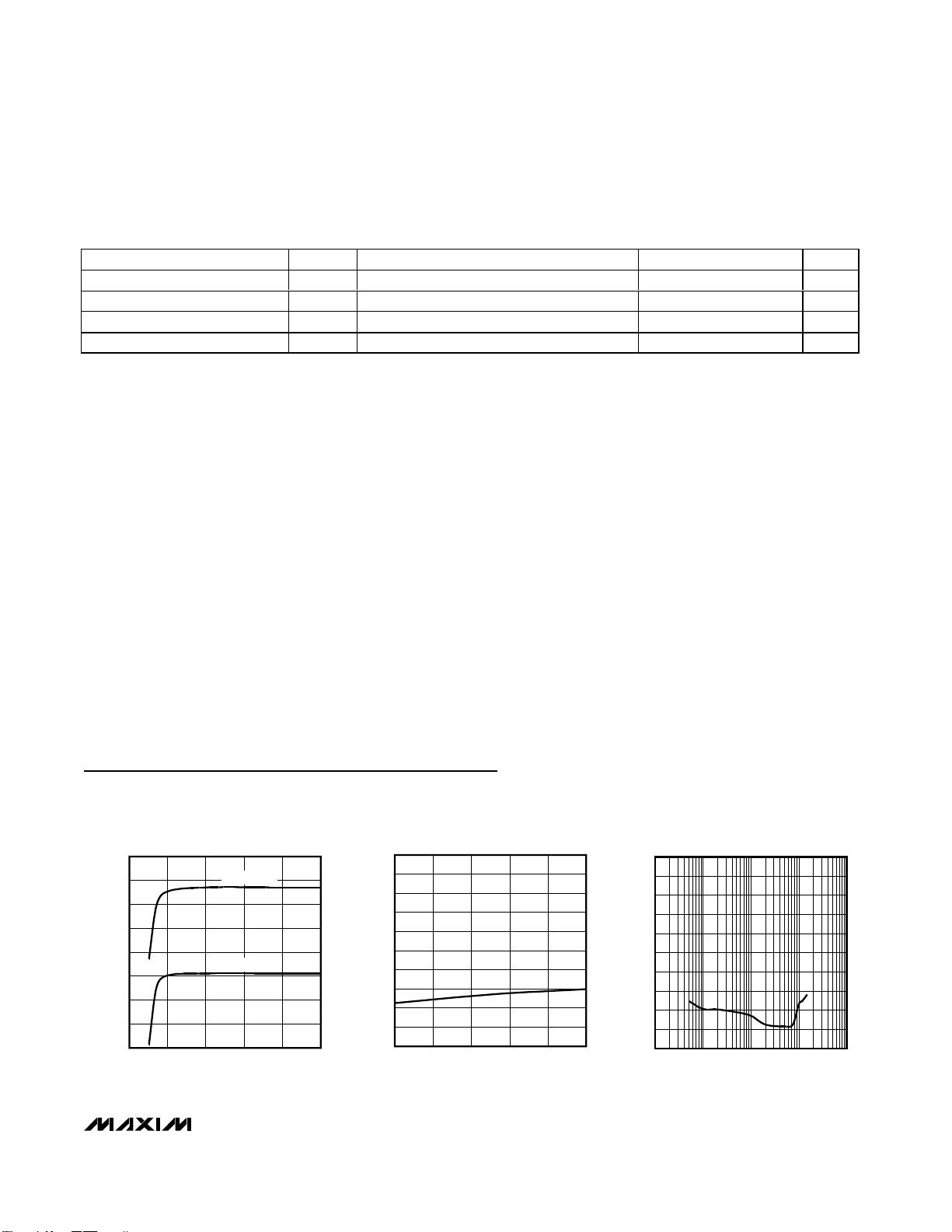
Typical Operating Characteristics
(VCC= +3.3V, TA = +25°C, unless otherwise noted.)
600
650
700
750
800
850
900
950
1000
01020304050
OUTPUT AMPLITUDE
vs. INPUT AMPLITUDE
MAX3272 toc01
VIN (mV
P-P
)
V
OUT
(mV
P-P
)
LEVEL = GND
LEVEL = OPEN
20
35
30
25
40
45
50
55
60
65
70
-40 10-15 35 6085
SUPPLY CURRENT
vs. AMBIENT TEMPERATURE
MAX3272 toc02
AMBIENT TEMPERATURE (°C)
SUPPLY CURRENT (mA)
0
6
4
2
8
10
12
14
16
18
20
110100 1000 10,000
DETERMINISTIC JITTER
vs. INPUT AMPLITUDE
MAX3272 toc03
INPUT AMPLITUDE (mV
P-P
)
DETERMINISTIC JITTER (ps
P-P
)
124.7
400
Page 4
MAX3272/MAX3272A
+3.3V, 2.5Gbps Low-Power
Limiting Amplifiers
4 _______________________________________________________________________________________
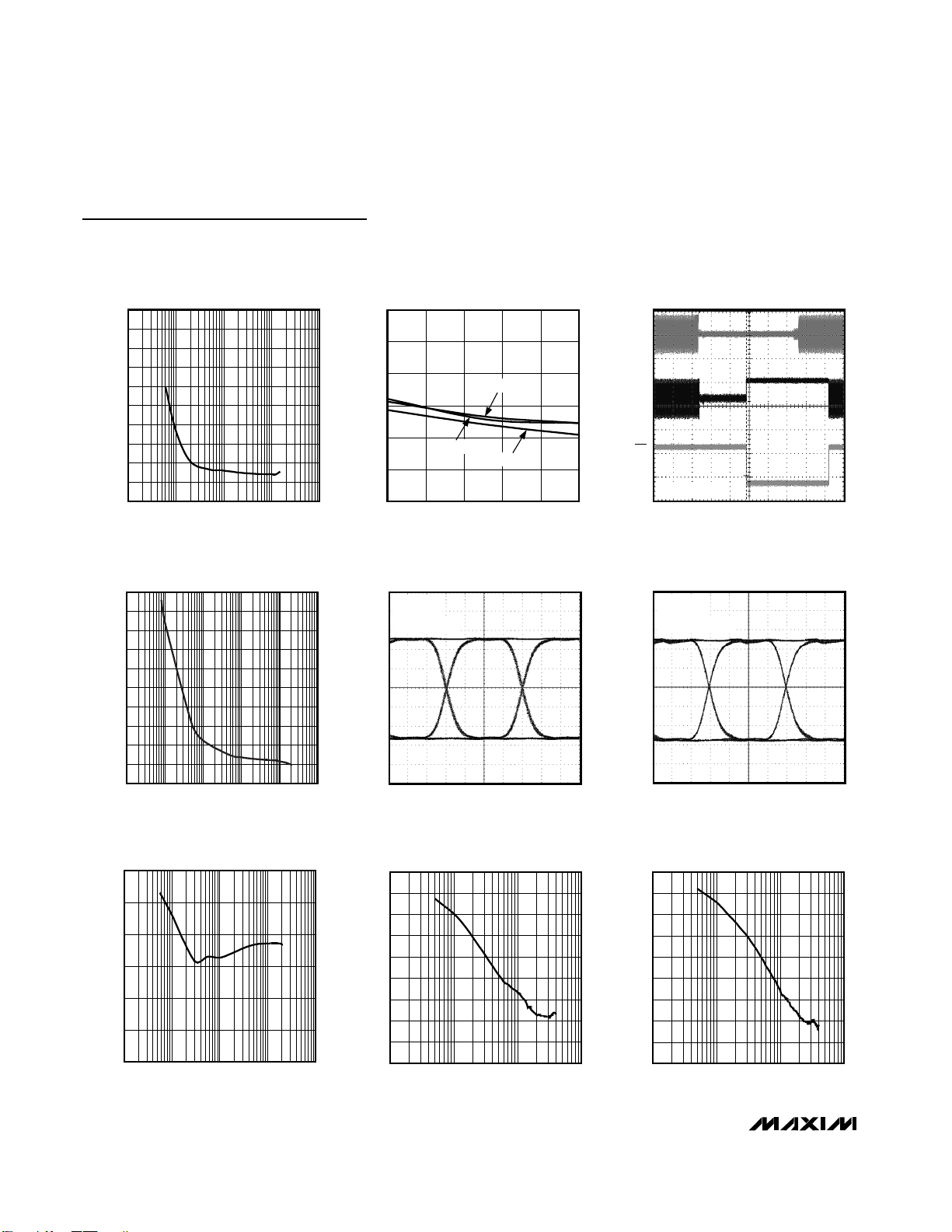
Typical Operating Characteristics (continued)
(VCC= +3.3V, TA = +25°C, unless otherwise noted.)
0
3
2
1
4
5
6
7
8
9
10
110100 1000 10,000
RANDOM JITTER vs. INPUT AMPLITUDE
MAX3272 toc04
INPUT AMPLITUDE (mV
p-p
)
RANDOM JITTER (ps
RMS
)
C
CLOS
= 0.01µF
V
OUT
V
IN
LOSS-OF-SIGNAL WITH SQUELCH
MAX3272 toc06
20µs/div
V
LOS
LOSS OF SIGNAL TRESHOLD vs. R
TH
XXXXXXXX
R
TH
(Ω)
LOS ASSERT (mV)
100k10k1k100
5
10
15
20
25
30
35
40
45
50
0
10 1M
DATA OUTPUT EYE DIAGRAM
(MINIMUM INPUT)
MAX3272 toc08
2.5Gbps
2
23
-1 PRBS
15mV
P-P
INPUT
100ps/div
150mV/
div
DATA OUTPUT EYE DIAGRAM
(MAXIMUM INPUT)
MAX3272 toc09
100ps/div
150mV/
div
2.5Gbps
2
23
-1 PRBS
1200mV
P-P
INPUT
0
20
10
40
30
50
60
1k 100k10k 1M 10M
POWER-SUPPLY NOISE REJECTION
vs. FREQUENCY
MAX3272 toc10
FREQUENCY (Hz)
POWER-SUPPLY NOISE REJECTION (dB)
0
10
5
25
20
15
40
35
30
45
10M 100M 1G 10G
INPUT RETURN LOSS vs. FREQUENCY
MAX3272 toc11
FREQUENCY (Hz)
INPUT RETURN LOSS (dB)
2.0
3.0
2.5
4.0
3.5
4.5
5.0
-40 85
LOS HYSTERESIS
vs. AMBIENT TEMPERATURE
MAX3272 toc05
AMBIENT TEMPERATURE (°C)
HYSTERESIS (dB)
10-15 35 60
RTH = 80Ω
RTH = 20kΩ
RTH = 1kΩ
0
10
5
25
20
15
40
35
30
45
10M 100M 1G 10G
OUTPUT RETURN LOSS vs. FREQUENCY
MAX3272 toc12
FREQUENCY (Hz)
OUTPUT RETURN LOSS (dB)
Page 5
MAX3272/MAX3272A
+3.3V, 2.5Gbps Low-Power
Limiting Amplifiers
_______________________________________________________________________________________ 5
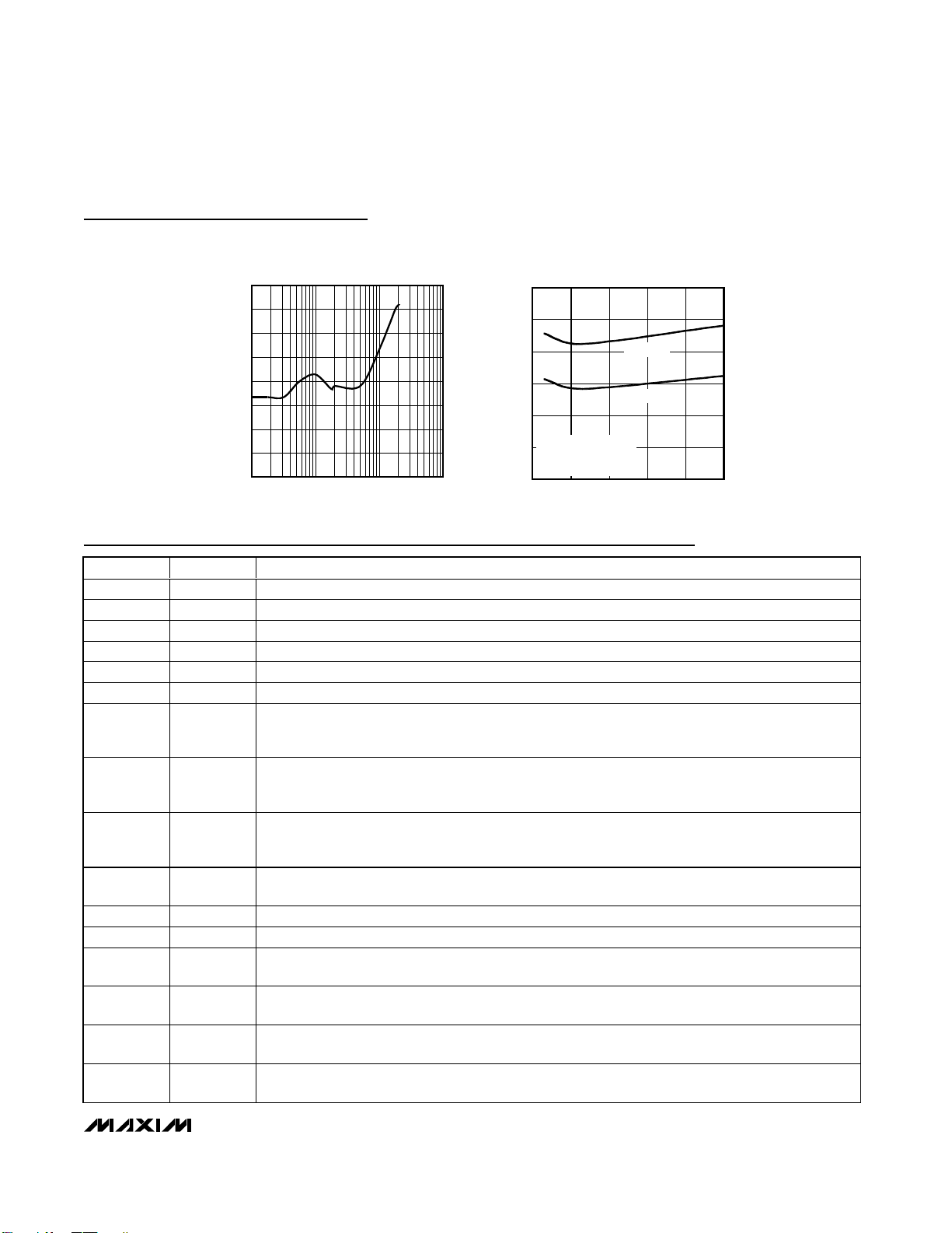
Pin Description
Typical Operating Characteristics (continued)
(VCC= +3.3V, TA = +25°C, unless otherwise noted.)
15.0
15.5
16.0
16.5
17.0
17.5
18.0
18.5
19.0
100k 1M 10M 100M
COMMON-MODE REJECTION RATIO
vs. FREQUENCY
MAX3272 toc13
FREQUENCY (Hz)
COMMON-MODE REJECTION RATIO (dB)
PIN NAME FUNCTION
1, 4, 17 GND Supply Ground
2 IN+ Noninverted Input Signal
3 IN- Inverted Input Signal
5THLoss-of-Signal Threshold Pin. Resistor to ground sets the LOS threshold.
6, 12, 15, 20
V
CC
Power Supply
7 CLOS LO S Ti m e- C onstant C ap aci tor C onnecti on. For S ON E T ap p l i cati ons, C
C L OS
= 0.01µF i s r ecom m end ed .
8
Squelch Input. The squelch function is disabled when SQUELCH is not connected or set to TTL low
level. When SQUELCH is set to TTL high level and LOS is asserted, the data outputs (OUT+, OUT-)
are forced to static levels.
9 LOS
Noninverted Loss-of-Signal Output. LOS is asserted TTL high when the signal drops below the assert
threshold set by the TH input. The MAX3272 does not have ESD protection on this pin. The
MAX3272A has ESD protection on this pin.
10 LOS
Inverted Loss-of-Signal Output. LOS is asserted TTL low when the signal drops below the assert
threshold set by the TH input. The MAX3272 does not have ESD protection on this pin. The
MAX3272A has ESD protection on this pin.
11 LEVEL
Output Current Level. When this pin is not connected, the CML output current is approximately
16mA. When this pin is connected to ground, the output current increases to about 20mA.
13 OUT- Inverted Data Output
14 OUT+ Noninverted Data Output
16 OUTPOL
Output Polarity Control Input. Connect to GND for an inversion of polarity through the limiting
amplifier and connect to V
CC
for normal operation.
18 CAZ2
Offset-Correction-Loop Capacitor Connection. A capacitor connected between this pin and CAZ1
extends the time constant of the offset correction loop. Typical value of C
AZ
is 0.1µF.
19 CAZ1
Offset-Correction-Loop Capacitor Connection. A capacitor connected between this pin and CAZ2
extends the time constant of the offset correction loop. Typical value of C
AZ
is 0.1µF.
EP
EXPOSED
PAD
Connect the exposed paddle to board ground for optimal electrical and thermal performance.
0
4
2
8
6
10
12
0 2500
LOS ASSERT AND DEASSERT LEVELS
vs. DATA RATE
MAX3272 toc14
DATA RATE (Mbps)
V
IN
(mV
P-P
)
1000500 1500 2000
2
23
- 1 PRBS PATTERN
R
TH
= 20kΩ
C
IN
= 0.1µF
DEASSERT
ASSERT
SQUELCH
Page 6

MAX3272/MAX3272A
Detailed Description
Figure 2 is a functional diagram of the MAX3272/
MAX3272A, comprising a CML input buffer, power
detector and loss-of- signal indicators, gain stage, offsetcorrection loop, and CML output buffer.
CML Input Buffer
The input buffer (Figure 3) provides 100Ω input impedance between IN+ and IN-. DC-coupling the inputs is
not recommended; this prevents the DC offset-correction circuitry from functioning properly.
Power Detect and
Loss-of-Signal Indicator
The MAX3272/MAX3272A are equipped with loss-of-signal (LOS) circuitry that indicates when the input signal is
below a programmable threshold, set by resistor RTHat
the TH pin (see the Typical Operating Characteristics for
appropriate resistor selection). An averaging peakpower detector compares the input signal amplitude
with this threshold and feeds the signal-detect information to the LOS outputs, which are internally terminated
to 8kΩ (Figure 4).
+3.3V, 2.5Gbps Low-Power
Limiting Amplifiers
6 _______________________________________________________________________________________
CML SUPPLY CURRENT (ICC)
V
CC
I
CC
I
OUT
50Ω
R
TH
50Ω
CONTROL
SQUELCH
OPEN
LEVEL
OPEN
MAX3272/
MAX3272A
Figure 1. Power-Supply Current Measurement
MAX3272/
MAX3272A
TTL
TTL
CONTROL
POWER
DETECTOR
IN+
IN-
100Ω
POWER DETECTOR AND
LOS INDICATOR
CML
INPUT
BUFFER
CML
OUTPUT
BUFFER
OFFSET
CORRECTION
0.1µF
LOWPASS
FILTER
LOS
SQUELCH
OUT+
OUT-
LEVEL
OUTPOL
LOS
CAZ1 CAZ2
TH CLOS
Figure 2. Functional Diagram
Page 7

Two control voltages V
ASSERT
, and V
DEASSERT
, define
the LOS assert and deassert levels. To prevent LOS
chatter in the region of the programmed threshold,
approximately 3.3dB of hysteresis is built into the LOS
assert/deassert function. Once asserted, LOS is not
deasserted until the input amplitude rises to the
required level (V
DEASSERT
).
To facilitate interfacing with +5V modules, the LOS and
LOS pins on the MAX3272 do not have internal ESD
protection. If ESD protection is desired, a low-capacitance Schottky diode or diode array structure, such as
the MAX3202E, is recommended (see the Typical
Operating Circuits).
The LOS and LOS pins on the MAX3272A include ESD
protection and, as a result, cannot be interfaced with
+5V modules.
Gain Stage
The high-bandwidth gain stage provides approximately
42dB of gain.
Offset-Correction Loop
Due to the high gain of the amplifier, the MAX3272/
MAX3272A are susceptible to DC offsets in the signal
path. In communications systems using NRZ data with
a 50% duty cycle, pulse-width distortion present in the
signal or generated by the transimpedance amplifier
appears as input offset and is removed by the offsetcancellation loop. An external capacitor is required
between CAZ1 and CAZ2 to decouple the offset-cancellation loop and determine the lower 3dB frequency
of the signal path.
MAX3272/MAX3272A
+3.3V, 2.5Gbps Low-Power
Limiting Amplifiers
_______________________________________________________________________________________ 7
Interface Schematics
IN+
IN-
110Ω
GND
ESD
STRUCTURES
V
CC
540Ω
540Ω
0.25pF
0.25pF
Figure 3. Input Circuit
GND
ESD
STRUCTURE
V
CC
LOS
8kΩ
Figure 4a. LOS Output Circuit for MAX3272
GND
ESD
STRUCTURE
V
CC
LOS
8kΩ
Figure 4b. LOS Output Circuit for MAX3272A
Page 8

CML Output Buffer
The MAX3272/MAX3272A CML output circuit (Figure 5)
provides high tolerance to impedance mismatches and
inductive connectors. The output current can be set to
two levels using the LEVEL pin. When LEVEL is unconnected, the output current is approximately 16mA.
Connecting LEVEL to ground sets the output current to
approximately 20mA. The squelch function is enabled
when the SQUELCH pin is set to a TTL high. This function holds OUT+ and OUT- to a static level whenever
the input signal amplitude drops below the loss-of-signal threshold. This circuit is also equipped with a polarity selector, programmed by the OUTPOL pin. When
this pin is connected to V
CC
, no inversion will occur.
When connected to ground, the output signal will be
inverted.
Design Procedure
Program the LOS Assert Threshold
External resistor RTHprograms the loss-of-signal
threshold. See the LOS Threshold vs. R
TH
graph in the
the Typical Operating Characteristics section to select
the appropriate resistor.
Select the Coupling Capacitors
When AC-coupling, input and output coupling capacitors (C
IN
and C
OUT
) should be selected to minimize the
receiver’s deterministic jitter. Jitter is decreased as the
input low-frequency cutoff (fIN) is decreased:
fIN= 1 / [2π(50)(CIN)]
For ATM/SONET or other applications using scrambled
NRZ data, select (C
IN
, C
OUT
) ≥ 0.1µF, which provides
f
IN
< 32kHz. For Fibre Channel, Gigabit Ethernet, or
other applications using 8B/10B data coding, select
(C
IN
, C
OUT
) ≥ 0.01µF, which provides fIN< 320kHz.
Refer to application note HFAN-1.1: Choosing AC-
Coupling Capacitors.
Select the Offset-Correction
Capacitor
The capacitor between CAZ1 and CAZ2 determines the
time constant of the signal path DC offset-cancellation
loop. To maintain stability, it is important to keep a onedecade separation between fINand the low-frequency
cutoff (fOC) associated with the DC offset-cancellation
circuit. For ATM/SONET or other applications using
scrambled NRZ data, fIN< 32kHz, so f
OCMAX
<
3.2kHz. Therefore, CAZ= 0.1µF (fOC= 2kHz). For Fibre
Channel or Gigabit Ethernet applications, leave pins
CAZ1 and CAZ2 open.
Program the LOS Time Constant
External capacitor C
CLOS
programs the LOS assert
and deassert times. When inputting data with many
consecutive identical digits (CIDs), a longer time constant may be advantageous, so LOS does not flag
incorrectly. In this case, connect the CLOS pin to a
0.01µF capacitor to set the assert time in the range of
2µs to 100µs. For scrambled data where the mark density is kept at 50%, a shorter time constant may be
desirable. Leave the CLOS pin open for a shorter time
constant of about 1µs.
MAX3272/MAX3272A
+3.3V, 2.5Gbps Low-Power
Limiting Amplifiers
8 _______________________________________________________________________________________
GND LEVEL
ESD
STRUCTURES
V
CC
50Ω 50Ω
OUT-
OUT+
Figure 5. CML Output Circuit
Page 9
Applications Information
Optical Hysteresis
In an optical receiver, the electrical power change at the
limiting amplifier is 2 times the optical power change.
As an example, if a receiver’s optical input power (x)
increases by a factor of two, and the preamplifier is linear, then the voltage input to the limiting amplifier also
increases by a factor of two.
The optical power change is 10log(2x / x) = 10log(2) =
+3dB.
At the limiting amplifier, the electrical power change is:
The MAX3272 typical voltage hysteresis is 3.3dB. This
provides an optical hysteresis of 1.65dB.
10log
2V / R
V/ R
10log(2 ) 20log(2) 6dB
IN
2
IN
IN2IN
2
()
===+
MAX3272/MAX3272A
+3.3V, 2.5Gbps Low-Power
Limiting Amplifiers
_______________________________________________________________________________________ 9
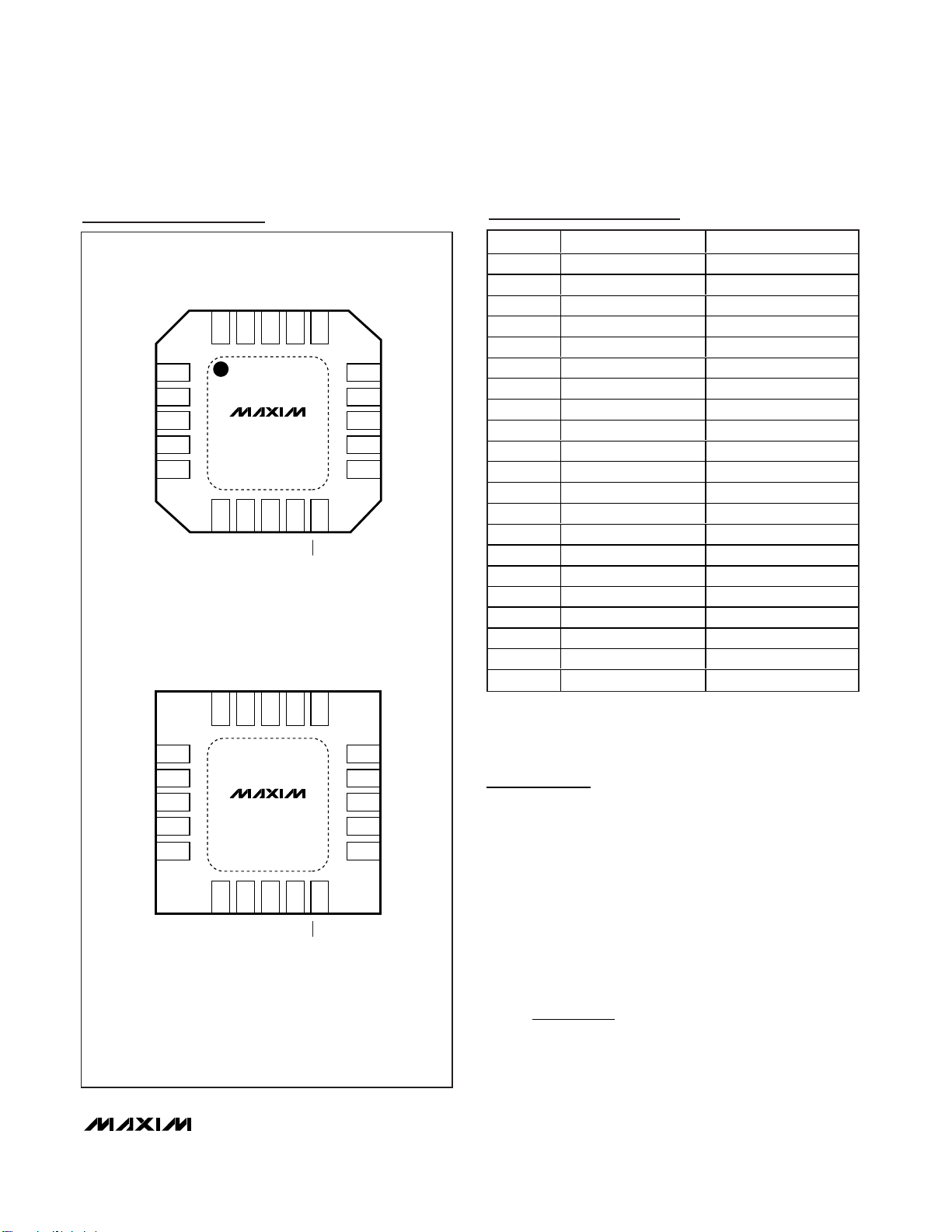
1
2
3
4
5
15
14
13
12
11
20 19 18 17 16
678910
GND
IN+
IN-
GND
NOTE: EXPOSED PAD MUST BE CONNECTED TO SUPPLY GROUND.
TH
V
CC
OUT+
OUT-
V
CC
LEVEL
VCCCAZ1
CAZ2
GND
OUTPOL
V
CC
CLOS
SQUELCH
LOS
LOS
TOP VIEW
QFN*
MAX3272/
MAX3272A
1
2
3
4
5
15
14
13
12
11
20 19 18 17 16
678910
GND
IN+
IN-
GND
NOTE: EXPOSED PAD MUST BE CONNECTED TO SUPPLY GROUND.
TH
V
CC
OUT+
OUT-
V
CC
LEVEL
VCCCAZ1
CAZ2
GND
OUTPOL
V
CC
CLOS
SQUELCH
LOS
LOS
THIN QFN*
MAX3272A
+
Pin Configuration
Pad Coordinates
PAD NAME
COORDINATES (µm)
1 GND 47, 836
2 IN+ 47, 603
3 IN- 47, 425
4 GND 47, 237
5TH 47, 47
6V
CC
255, -154
7 CLOS 436, -154
8 SQUELCH 645, -154
9 LOS 850, -154
10 LOS 1063, -154
11 LEVEL 1331, 37
12 V
CC
1331, 212
13 OUT- 1331, 421
14 OUT+ 1331, 573
15 V
CC
1331, 780
16 OUTPOL 1119, 1042
17 GND 957, 1042
18 CAZ2 773, 1042
19 CAZ1 583, 1042
20 N.C. 422, 1042
21 V
CC
268, 1042
Coordinates are for the center of the pad.
Coordinate 0, 0 is the lower left corner of the passivation opening for pad 5.
Page 10

MAX3272/MAX3272A
+3.3V, 2.5Gbps Low-Power
Limiting Amplifiers
10 ______________________________________________________________________________________
+3.3V
+3.3V
+3.3V
C
AZ
CAZ1
OUTPOL
CAZ2 V
CC
0.1µF
0.1µF
TH SQUELCH
C
CLOS
*THE MAX3202E PROVIDES ESD PROTECTION ON THE LOS PIN
CLOS
100Ω
IN-
IN+
OUT+
SDI+ SDO+
V
CC
SDO-
SCLKO-
SCLKO+
SDI-
GND
CDR
OUT-
MAX3271
MAX3272
MAX3873
LOSGND
LOSS
OF
SIGNAL
LOS
R
TH
LEVEL
+3.3V
V
CC
I/01
GND
MAX3202E*
Typical Operating Circuit (continued)
Wire Bonding Die
For high-current density and reliable operation, the
MAX3272 uses gold metallization. Make connections to
the dice with gold wire only, and use ball-bonding techniques (wedge bonding is not recommended). Die pad
dimensions are 94.4 microns by 94.4 microns. Die
thickness is 15 mils (0.375mm).
Page 11

MAX3272/MAX3272A
+3.3V, 2.5Gbps Low-Power
Limiting Amplifiers
______________________________________________________________________________________ 11
Chip Information
V
CC
(PAD 21)
N.C.
(PAD 20)
CAZ1
(PAD 19)
CAZ2
(PAD 18)
GND
(PAD 17)
OUTPOL
(PAD 16)
V
CC
(PAD 6)
CLOS
(PAD 7)
SQUELCH
(PAD 8)
LOS
(PAD 9)
LOS
(PAD 10)
V
CC
(PAD 15)
OUT+
(PAD 14)
OUT(PAD 13)
V
CC
(PAD 12)
LEVEL
(PAD 11)
GND
(PAD 1)
IN+
(PAD 2)
IN-
(PAD 3)
GND
(PAD 4)
TH
(PAD 5)
62 mils
1.57mm
66 mils
1.68mm
TRANSISTOR COUNT: 726
PROCESS: SiGe Bipolar
SUBSTRATE: Insulator, Connect to GND
DIE SIZE: 1.68mm
✕ 1.57mm
DIE THICKNESS: 15 mils
Page 12

MAX3272/MAX3272A
+3.3V, 2.5Gbps Low-Power
Limiting Amplifiers
12 ______________________________________________________________________________________
12,16,20, 24L QFN.EPS
E
1
2
21-0106
PACKAGE OUTLINE
12,16,20,24L QFN, 4x4x0.90 MM
Package Information
(The package drawing(s) in this data sheet may not reflect the most current specifications. For the latest package outline information,
go to www.maxim-ic.com/packages
.)
Page 13

MAX3272/MAX3272A
+3.3V, 2.5Gbps Low-Power
Limiting Amplifiers
______________________________________________________________________________________ 13
E
2
2
21-0106
PACKAGE OUTLINE
12,16,20,24L QFN, 4x4x0.90 MM
Package Information (continued)
(The package drawing(s) in this data sheet may not reflect the most current specifications. For the latest package outline information,
go to www.maxim-ic.com/packages
.)
Page 14

MAX3272/MAX3272A
+3.3V, 2.5Gbps Low-Power
Limiting Amplifiers
Maxim cannot assume responsibility for use of any circuitry other than circuitry entirely embodied in a Maxim product. No circuit patent licenses are
implied. Maxim reserves the right to change the circuitry and specifications without notice at any time.
14 ____________________Maxim Integrated Products, 120 San Gabriel Drive, Sunnyvale, CA 94086 408-737-7600
© 2004 Maxim Integrated Products Printed USA is a registered trademark of Maxim Integrated Products.
Package Information (continued)
(The package drawing(s) in this data sheet may not reflect the most current specifications. For the latest package outline information,
go to www.maxim-ic.com/packages
.)
24L QFN THIN.EPS
C
1
2
21-0139
PACKAGE OUTLINE
12, 16, 20, 24L THIN QFN, 4x4x0.8mm
C
2
2
21-0139
PACKAGE OUTLINE
12, 16, 20, 24L THIN QFN, 4x4x0.8mm
 Loading...