_______________General Description
The MAX3270 is a complete Clock Recovery and Data
Retiming IC for 155Mbps and 622Mbps SDH/SONET
and ATM applications. The MAX3270 meets Bellcore
and CCITT jitter tolerance specifications ensuring errorfree data recovery. Recovered clock and data are
phase aligned using a fully integrated phase-locked
loop (PLL). An output frequency monitor (FM) is included to detect loss of PLL acquisition or a loss of input
data.
The MAX3270 has differential ECL input and output
interfaces, so it is less susceptible to noise in a highfrequency environment. The fully integrated PLL
includes an integrated phase-frequency detector that
eliminates the need for external references.
________________________Applications
155Mbps (STM-1/OC-3)/622Mbps (STM-4/
OC-12) SDH/SONET Transmission Systems
155Mbps/622Mbps ATM/SONET Access Nodes
Add/Drop Multiplexers
Cross-Connects
____________________________Features
♦ Supports Both 155Mbps and 622Mbps Clock
Recovery and Data Retiming
♦ Fully Integrated Phase/Frequency Detector
♦ Capable of Switching to an External Clock
♦ Differential 100K ECL Data and Clock I/Os
♦ Output Monitor Provides Lock Detection
♦ No External Reference Clock Required
Pin Configuration appears at end of data sheet.
MAX3270
155Mbps/622Mbps Clock Recovery and
Data Retiming IC with Fully Integrated
Phase/Frequency Detector
________________________________________________________________
Maxim Integrated Products
1
MAX3270
50Ω
50Ω
50Ω
50Ω 50Ω
450Ω
11
+5V
3
4
41
42
13
18
20
14
17219 3839
VTTL
SDIP
RCON
CRP
FILP
FILG
FILN
FM
RCOP
RDOP
RDON
26
25
31
30
2.2µF
20Ω
-4.5V
2.2µF
20Ω
28
9
8
10
6
SDIN
PHADJ
-2V
-2V
-2V
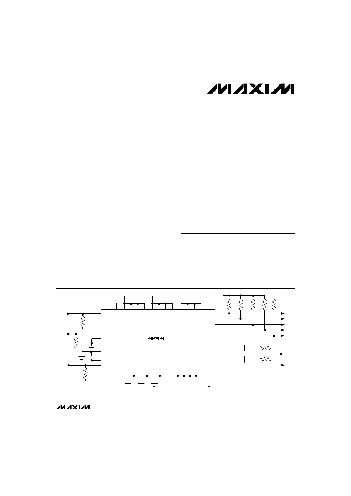
EXCS AND CRS ARE CONNECTED FOR
622Mbps OPERATION.
BYPASS SUPPLIES WITH 0.1µF AND 0.01µF CAPACITORS.
DECOUPLE AVEE1, AVEE2, AND GVEE SUPPLY PINS.
50Ω
50Ω
DVCC
DVCC
AVEE1
AVEE2
GVEE
DVEE
DVEE
DVEE
DVEE
DVEE
DVCC
DVCC
AVCC
AVCC
AVCC
AVCC
OVCC
OVCC
OVCC
OVCC
16 15 57 272932
-2V
+5V
24
VR
EXCS
CRS
RST
EXC
12
-4.5V-4.5V -4.5V
-4.5V
DIGITAL
SUPPLY
ANALOG SUPPLY
1
35 36 22 21 34
___________________________________________________Typical Operating Circuit
Call toll free 1-800-998-8800 for free samples or literature.
19-0379; Rev 0; 3/95
PART
MAX3270EMH -40°C to +85°C
TEMP. RANGE PIN-PACKAGE
44 MQFP
______________Ordering Information

MAX3270
155Mbps/622Mbps Clock Recovery and
Data Retiming IC with Fully Integrated
Phase/Frequency Detector
2 _______________________________________________________________________________________
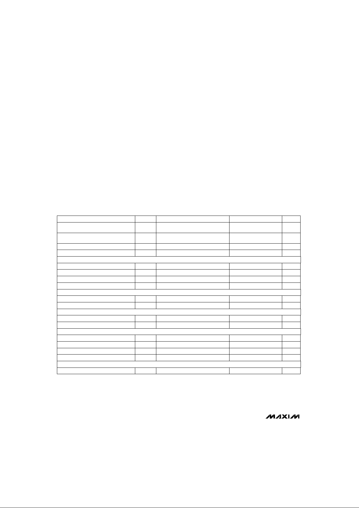
ABSOLUTE MAXIMUM RATINGS
ELECTRICAL CHARACTERISTICS
(VEE= -4.5V ±5%, VTTL = 5V ±5%, TA= -40°C to +85°C, unless otherwise noted.)
Stresses beyond those listed under “Absolute Maximum Ratings” may cause permanent damage to the device. These are stress ratings only, and functional
operation of the device at these or any other conditions beyond those indicated in the operational sections of the specifications is not implied. Exposure to
absolute maximum rating conditions for extended periods may affect device reliability.
Supply Voltages
VTTL to GND .....................................................-0.5V to +8.0V
V
CC
to GND.......................................................-0.5V to +8.0V
V
EE
to GND........................................................-8.0V to +0.5V
SDIP, SDIN, EXC...................................................-8.0V to +0.5V
RDOP, RDON, RCOP, RCON, CRP.......................-8.0V to +0.5V
EXCS, RST, CRS....................................................-0.5V to +8.0V
FILP, FILG, FILN....................................................-8.0V to +0.5V
PHADJ, VR ............................................................-8.0V to +8.0V
FM .........................................................................-8.0V to +8.0V
Input Differential Voltage Level, SDIP, SDIN ......................+3.0V
Continuous Power Dissipation (T
A
= +85°C).......................1.3W
Operating Temperature Range ...........................-40°C to +85°C
Storage Temperature Range.............................-55°C to +150°C
Lead Temperature (soldering, 10sec).............................+300°C
VR = PHADJ = 0, T
A
= +25°C
VTTL = 5.00V, VIN = 0.8V
VTTL = 5.00V, VIN = 2V
Loaded with 50Ω to -2V
Loaded with 470Ω to V
EE
Loaded with 470Ω to V
EE
VIN= VOL(typ)
VIN= VOH(typ)
Loaded with 50Ω to -2V
CONDITIONS
µA010I
BIAS
Input Bias Current
µA040I
IL
Input Low Current
µA040I
IH
Input High Current
V0.8V
IL
Input Low Voltage
V2V
IH
Input High Voltage
mV-1830 -1705 -1620V
OL
Output Low Voltage
mV-1025 -955 -870V
OH
Output High Voltage
mV-1830 -1705 -1550V
OL
Output Low Voltage
mA2.4 5I
TTL
Static Supply Current from VTTL
V-4.725 -4.50 -4.275V
EE
V4.75 5.00 5.25V
TTL
Positive Voltage Supply
(with respect to ground)
Negative Voltage Supply
(with respect to ground)
mV-1025 -955 -870V
OH
Output High Voltage
nA-100 100I
IL
Input Low Current
µA0 100I
IH
Input High Current
mA150 210I
VEE
Static Supply Current from V
EE
mV-1165 -870V
IH
Input High Voltage
mV-1830 -1475V
IL
Input Low Voltage
UNITSMIN TYP MAXSYMBOLPARAMETER
PHASE ADJUST INPUTS: PHADJ, VR
TTL INPUTS: CRS, RST, EXCS
LOW-POWER ECL OUTPUT: CRP
ECL OUTPUTS: RCOP, RCON, RDOP, RDON
ECL INPUTS: EXC, SDIP, SDIN

MAX3270
155Mbps/622Mbps Clock Recovery and
Data Retiming IC with Fully Integrated
Phase/Frequency Detector
_______________________________________________________________________________________ 3
AC ELECTRICAL CHARACTERISTICS (continued)
(VEE= -4.5V, VTTL = 5V, TA= 25°C, unless otherwise noted.)
PHADJ = 0
Loaded with 50Ω to -2V and
5pF to GND
FILP and FILN shorted
FILP - FILN = 1.6V
FILP - FILN = 1.6V
FILP and FILN open
FILP and FILN shorted,
PFD = neutral state
ft= 622.08MHz
CONDITIONS
rad/V2K
PHADJ
Phase Offset Sensitivity, ∆Φ/∆PHADJ
mA/V1.25GmTransconduction Gain of Filter Amplifier
mV/rad192KDPhase-Detector Gain
MHz/V75K
O
Incremental Tuning Sensitivity
(Incremental Slope, ∆f/∆Vt)
MHz622.08F
O
Frequency of VCO
V/V0.95 1.05GFMGain of the Monitor Amplifier
ps600tr, t
f
Transition Time 20% to 80%
kHz/V550K
OV
Frequency Sensitivity to
Power-Supply Voltage
MHz/V3.75 6K
O
Mean Frequency Sensitivity
MHz610DF
O
Frequency Range
dB21 26GOLFilter Amplifier Open-Loop Voltage Gain
MHz38.00 39.50F
O
Center Frequency
UNITSMIN TYP MAXSYMBOLPARAMETER
175
180
185
190
150
-40 80
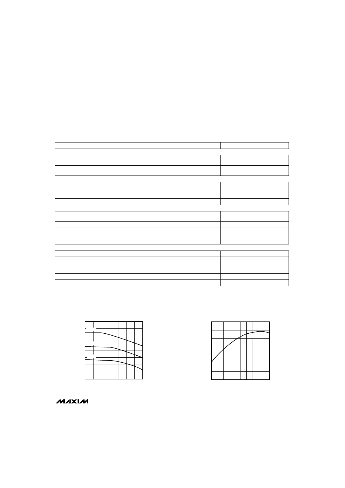
VEE SUPPLY CURRENT
vs. TEMPERATURE
155
170
MAX3270-TOC9
TEMPERATURE (°C)
V
EE
SUPPLY CURRENT (mA)
0 40 60 100-20 20
165
160
-4.75V
-4.5V
-4.25V
__________________________________________Typical Operating Characteristics
PHADJ = 0, FILP and FILN shorted mV-35 35V
O
Output Offset Voltage of the
Monitor Amplifier
Loaded with 50Ω to -2V and
5pF to GND
ps100TDTime Difference between RDO and RCO
ECL OUTPUTS: RDOP, RDON, RCOP, RCON
VCO TEST PARAMETERS; CPR OUTPUT
PLL ELECTRICAL SPECIFICATIONS
PFD AND FILTER AMPLIFIER TEST LEVELS
38.8
38.9
39.0
38.3
0 60 80 100
CRP FREE-RUNNING FREQUENCY (VCO/16)
vs. DIE TEMPERATURE
38.4
38.7
MAX3270-TOC5
TEMPERATURE (°C)
FREQUENCY (MHz)
20 40 50 70 9010 30
38.6
38.5
MEASURED

MAX3270
155Mbps/622Mbps Clock Recovery and
Data Retiming IC with Fully Integrated
Phase/Frequency Detector
4 _______________________________________________________________________________________
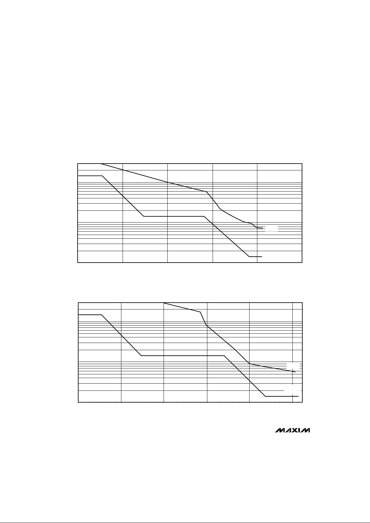
__________________________________________Typical Operating Characteristics
0.1
10 1k 10k 100k 1M
JITTER TOLERANCE
(155Mbps, 2
23
-1 PRBS)
1.0
10.0
MAX3270-TOC1
FREQUENCY (Hz)
AMPLITUDE (UI p-p)
100
DATA
BELLCORE
MASK
0.1
10 1k 10k 100k 1M
JITTER TOLERANCE
(622Mbps, 2
23
-1 PRBS)
1.0
10.0
MAX3270-TOC2
FREQUENCY (Hz
)
AMPLITUDE (UI p-p)
100
DATA
BELLCORE
MASK
 Loading...