

Page 1
现货库存、技术资料、百科信息、热点资讯,精彩尽在鼎好!
19-0379; Rev 0; 3/95
155Mbps/622Mbps Clock Recovery and
Data Retiming IC with Fully Integrated
_______________General Description
The MAX3270 is a complete Clock Recovery and Data
Retiming IC for 155Mbps and 622Mbps SDH/SONET
and ATM applications. The MAX3270 meets Bellcore
and CCITT jitter tolerance specifications ensuring errorfree data recovery. Recovered clock and data are
phase aligned using a fully integrated phase-locked
loop (PLL). An output frequency monitor (FM) is included to detect loss of PLL acquisition or a loss of input
data.
The MAX3270 has differential ECL input and output
interfaces, so it is less susceptible to noise in a highfrequency environment. The fully integrated PLL
includes an integrated phase-frequency detector that
eliminates the need for external references.
________________________Applications
155Mbps (STM-1/OC-3)/622Mbps (STM-4/
OC-12) SDH/SONET Transmission Systems
155Mbps/622Mbps ATM/SONET Access Nodes
Add/Drop Multiplexers
Cross-Connects
Phase/Frequency Detector
____________________________Features
♦ Supports Both 155Mbps and 622Mbps Clock
Recovery and Data Retiming
♦ Fully Integrated Phase/Frequency Detector
♦ Capable of Switching to an External Clock
♦ Differential 100K ECL Data and Clock I/Os
♦ Output Monitor Provides Lock Detection
♦ No External Reference Clock Required
______________Ordering Information
PART
MAX3270EMH -40°C to +85°C
Pin Configuration appears at end of data sheet.
TEMP. RANGE PIN-PACKAGE
44 MQFP
MAX3270
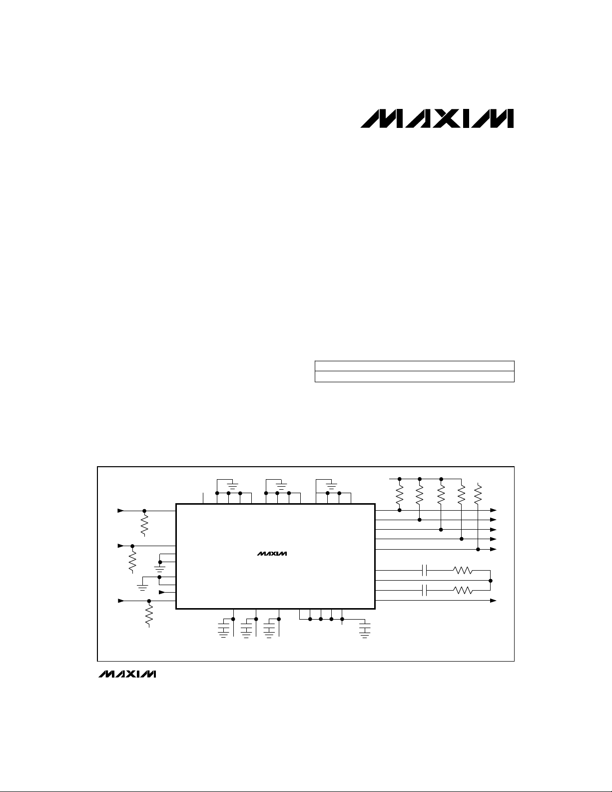
___________________________________________________Typical Operating Circuit
3
SDIP
50Ω
-2V
4
SDIN
41
PHADJ
50Ω
-2V
50Ω
EXCS AND CRS ARE CONNECTED FOR
622Mbps OPERATION.
42
VR
13
EXCS
18
CRS
20
+5V
-2V
RST
14
EXC
________________________________________________________________
+5V
17219 3839
11
VTTL
DVCC
DVCC
16 15 57 272932
AVCC
DVCC
AVCC
DVCC
AVCC
AVCC
24
OVCC
OVCC
OVCC
MAX3270
AVEE1
AVEE2
GVEE
DVEE
DVEE
DVEE
DVEE
DVEE
1
12
-4.5V-4.5V -4.5V
ANALOG SUPPLY
35 36 22 21 34
-4.5V
DIGITAL
SUPPLY
-2V
50Ω
50Ω
50Ω 50Ω
26
RDOP
25
OVCC
RDON
31
RCOP
30
RCON
28
CRP
9
FILP
FILG
FILN
FM
BYPASS SUPPLIES WITH 0.1µF AND 0.01µF CAPACITORS.
DECOUPLE AVEE1, AVEE2, AND GVEE SUPPLY PINS.
2.2µF
8
10
2.2µF
6
Maxim Integrated Products
-4.5V
450Ω
20Ω
20Ω
Call toll free 1-800-998-8800 for free samples or literature.
1
Page 2

155Mbps/622Mbps Clock Recovery and
Data Retiming IC with Fully Integrated
Phase/Frequency Detector
ABSOLUTE MAXIMUM RATINGS
Supply Voltages
VTTL to GND .....................................................-0.5V to +8.0V
to GND.......................................................-0.5V to +8.0V
V
CC
to GND........................................................-8.0V to +0.5V
V
EE
SDIP, SDIN, EXC...................................................-8.0V to +0.5V
RDOP, RDON, RCOP, RCON, CRP.......................-8.0V to +0.5V
EXCS, RST, CRS....................................................-0.5V to +8.0V
FILP, FILG, FILN....................................................-8.0V to +0.5V
MAX3270
Stresses beyond those listed under “Absolute Maximum Ratings” may cause permanent damage to the device. These are stress ratings only, and functional
operation of the device at these or any other conditions beyond those indicated in the operational sections of the specifications is not implied. Exposure to
absolute maximum rating conditions for extended periods may affect device reliability.
ELECTRICAL CHARACTERISTICS
(VEE= -4.5V ±5%, VTTL = 5V ±5%, TA= -40°C to +85°C, unless otherwise noted.)
PHADJ, VR ............................................................-8.0V to +8.0V
FM .........................................................................-8.0V to +8.0V
Input Differential Voltage Level, SDIP, SDIN ......................+3.0V
Continuous Power Dissipation (T
Operating Temperature Range ...........................-40°C to +85°C
Storage Temperature Range.............................-55°C to +150°C
Lead Temperature (soldering, 10sec).............................+300°C
= +85°C).......................1.3W
A
Positive Voltage Supply
(with respect to ground)
Negative Voltage Supply
(with respect to ground)
Static Supply Current from VTTL
Static Supply Current from V
ECL INPUTS: EXC, SDIP, SDIN
Input High Voltage
Input Low Voltage
Input High Current
Input Low Current
ECL OUTPUTS: RCOP, RCON, RDOP, RDON
Output High Voltage
Output Low Voltage
LOW-POWER ECL OUTPUT: CRP
Output High Voltage
Output Low Voltage
TTL INPUTS: CRS, RST, EXCS
Input High Voltage
Input Low Voltage
Input High Current
Input Low Current
PHASE ADJUST INPUTS: PHADJ, VR
Input Bias Current
EE
TTL
EE
TTL
VEE
IH
IL
VIN= VOH(typ)
IH
VIN= VOL(typ)
IL
Loaded with 50Ω to -2V
OH
Loaded with 50Ω to -2V
OL
Loaded with 470Ω to V
OH
Loaded with 470Ω to V
OL
IH
IL
VTTL = 5.00V, VIN = 2V
IH
VTTL = 5.00V, VIN = 0.8V
IL
VR = PHADJ = 0, T
BIAS
CONDITIONS
EE
EE
= +25°C
A
UNITSMIN TYP MAXSYMBOLPARAMETER
V4.75 5.00 5.25V
V-4.725 -4.50 -4.275V
mA2.4 5I
mA150 210I
mV-1165 -870V
mV-1830 -1475V
µA0 100I
nA-100 100I
mV-1025 -955 -870V
mV-1830 -1705 -1550V
mV-1025 -955 -870V
mV-1830 -1705 -1620V
V2V
V0.8V
µA040I
µA040I
µA010I
2 _______________________________________________________________________________________
Page 3
155Mbps/622Mbps Clock Recovery and
Data Retiming IC with Fully Integrated
Phase/Frequency Detector
AC ELECTRICAL CHARACTERISTICS (continued)
(VEE= -4.5V, VTTL = 5V, TA= 25°C, unless otherwise noted.)
MAX3270
CONDITIONS
UNITSMIN TYP MAXSYMBOLPARAMETER
ECL OUTPUTS: RDOP, RDON, RCOP, RCON
Transition Time 20% to 80%
Loaded with 50Ω to -2V and
f
5pF to GND
Loaded with 50Ω to -2V and
5pF to GND
ps600tr, t
ps100TDTime Difference between RDO and RCO
PFD AND FILTER AMPLIFIER TEST LEVELS
Output Offset Voltage of the
Monitor Amplifier
PHADJ = 0, FILP and FILN shorted mV-35 35V
O
PHADJ = 0
FILP and FILN open
V/V0.95 1.05GFMGain of the Monitor Amplifier
dB21 26GOLFilter Amplifier Open-Loop Voltage Gain
VCO TEST PARAMETERS; CPR OUTPUT
Center Frequency
Frequency Range
Mean Frequency Sensitivity
Frequency Sensitivity to
Power-Supply Voltage
FILP and FILN shorted,
O
PFD = neutral state
FILP - FILN = 1.6V
O
FILP - FILN = 1.6V
O
FILP and FILN shorted
OV
MHz38.00 39.50F
MHz610DF
MHz/V3.75 6K
kHz/V550K
PLL ELECTRICAL SPECIFICATIONS
Frequency of VCO
Incremental Tuning Sensitivity
(Incremental Slope, ∆f/∆Vt)
O
O
ft= 622.08MHz
MHz622.08F
MHz/V75K
mV/rad192KDPhase-Detector Gain
mA/V1.25GmTransconduction Gain of Filter Amplifier
Phase Offset Sensitivity, ∆Φ/∆PHADJ
PHADJ
rad/V2K
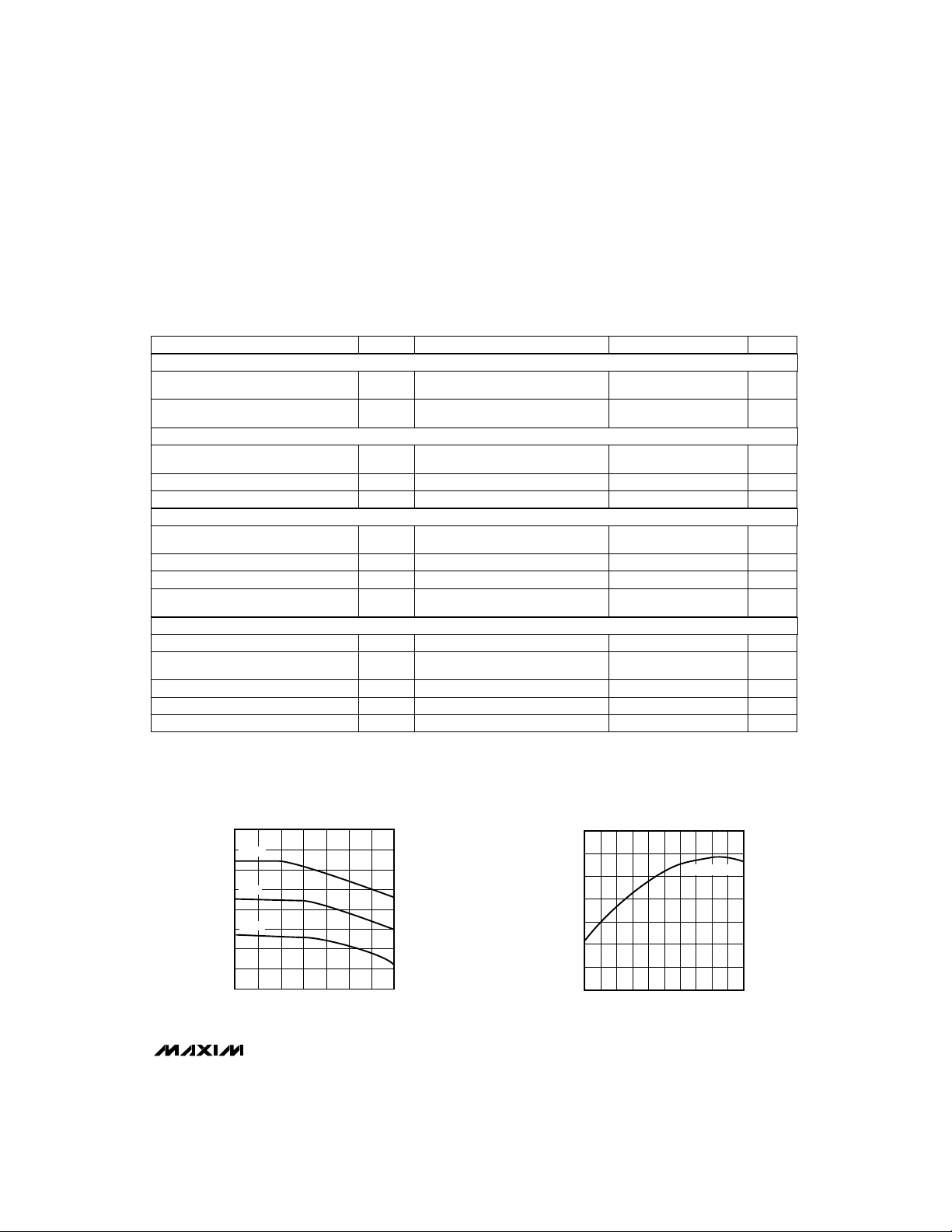
__________________________________________Typical Operating Characteristics
VEE SUPPLY CURRENT
190
185
180
175
170
165
SUPPLY CURRENT (mA)
160
EE
V
155
150
-40 80
vs. TEMPERATURE
-4.75V
-4.5V
-4.25V
0 40 60 100-20 20
TEMPERATURE (°C)
_______________________________________________________________________________________ 3
MAX3270-TOC9
CRP FREE-RUNNING FREQUENCY (VCO/16)
39.0
38.9
38.8
38.7
38.6
FREQUENCY (MHz)
38.5
38.4
38.3
vs. DIE TEMPERATURE
0 60 80 100
20 40 50 70 9010 30
TEMPERATURE (°C)
MEASURED
MAX3270-TOC5
Page 4
155Mbps/622Mbps Clock Recovery and
)
Data Retiming IC with Fully Integrated
Phase/Frequency Detector
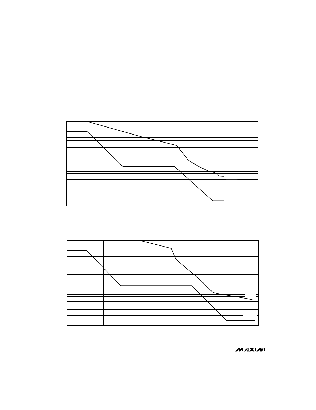
__________________________________________Typical Operating Characteristics
10.0
MAX3270
1.0
AMPLITUDE (UI p-p)
0.1
10 1k 10k 100k 1M
10.0
100
JITTER TOLERANCE
(155Mbps, 2
FREQUENCY (Hz)
JITTER TOLERANCE
(622Mbps, 2
23
-1 PRBS)
23
-1 PRBS)
DATA
BELLCORE
MASK
MAX3270-TOC1
MAX3270-TOC2
1.0
AMPLITUDE (UI p-p)
0.1
10 1k 10k 100k 1M
4 _______________________________________________________________________________________
100
FREQUENCY (Hz
DATA
BELLCORE
MASK
Page 5

155Mbps/622Mbps Clock Recovery and
Data Retiming IC with Fully Integrated
Phase/Frequency Detector
__________________________________________Typical Operating Characteristics
MAX3270
155Mbps RECOVERED CLOCK AND
RETIMED DATA (SINGLE ENDED)
RECOVERED CLOCK JITTER
RF = 20Ω
= 2.2µF
C
F
7
-1 PRBS, 5.1ps RMS)
10ps/div
(155Mbps, 2
Mean 40.61ns
RMS∆ 5.13ps
PkPk 45.6ps
2ns/div
µ±1σ 68.961%
µ±2σ 95.844%
µ±3σ 99.717%
622Mbps RECOVERED CLOCK AND
RETIMED DATA (SINGLE ENDED)
DATA
CLOCK
RECOVERED CLOCK JITTER
(155Mbps, 1-0 PATTERN, 4.7ps RMS)
RF = 20Ω
= 2.2µF
C
F
10ps/div
Mean 40.65ns
RMS∆ 4.7ps
PkPk 38.4ps
µ±1σ 69.674%
µ±2σ 95.558%
µ±3σ 99.698%
500ps/div
RECOVERED CLOCK JITTER
RF = 20Ω
= 2.2µF
C
F
7
-1 PRBS 9.0ps RMS)
10ps/div
(622Mbps 2
Mean 38.68ns
RMS∆ 9.049ps
PkPk 79.4ps
DATA
CLOCK
µ±1σ 69.747%
µ±2σ 95.453%
µ±3σ 99.582%
_______________________________________________________________________________________
5
Page 6

155Mbps/622Mbps Clock Recovery and
Data Retiming IC with Fully Integrated
Phase/Frequency Detector
______________________________________________________________Pin Description
PIN
Guard-Ring Negative Supply to Substrate: -4.5VGVEE1
Negative Supply for Input Buffers: -4.5VAVEE12
Serial Data Input: 155Mbps or 622Mbps. Differential ECL Positive.SDIP3
Serial Data Input: 155Mbps or 622Mbps. Differential ECL Negative.SDIN4
MAX3270
FM6
14 EXC External Clock. Single-ended ECL input.
15, 16 AVCC Ground for VCO: 0V
17, 19, 38,
39
18 CRS
20 RST Resets all digital flip-flops, TTL input. Reset is assert when low.
21, 22, 34,
35, 36
23, 33, 37,
40, 43, 44
24, 27, 29,
32
25 RDON Negative Recovered Data Output, differential ECL output: 155Mbps or 622Mbps.
26 RDOP Positive Recovered Data Output, differential ECL output: 155Mbps or 622Mbps.
28 CRP Clock-Reference Output Divide-by-4. ECL low-power single-ended: 38Mbps or 155Mbps.
30 RCON Negative Recovered Clock Output, differential ECL output: 155Mbps or 622Mbps.
31 RCOP Positive Recovered Clock Output, differential ECL output: 155Mbps or 622Mbps.
41 PHADJ
42 VR Phase Reference Voltage: 0V. The PHADJ pin compares to this voltage. Set to ground.
DVCC Digital Ground for Mux: 0V
DVEE Digital Negative Supply: -4.5V
N.C. No Connection
OVCC Output Driver Ground: 0V
Ground for Input Buffers: 0VAVCC5
Frequency Monitor Output. This pin monitors the input voltage to the VCO. When the PLL is locked,
the pin will be ≅ 0V.
Guard-Ring Positive Supply to Epi: 0VAVCC7
Loop Filter Ground. This pin connects to an external filter.FILG8
Loop Filter Positive. This pin connects to an external filter.FILP9
Loop Filter Negative. This pin connects to an external filter.FILN10
TTL Positive Supply: +5.0VVTTL11
Negative Supply for VCO: -4.5VAVEE212
External Clock-Select TTL Input. A logical high selects the external clock.EXCS13
Clock-Rate Select TTL Input. This selects the clock rate to be either 155Mbps or 622Mbps. A logichigh level selects the 622Mbps mode.
Phase Adjust. This is an analog adjustment that varies the static phase between the input data and
the recovered clock. If not used, this input should be grounded. The range is from -1V to 1V.
FUNCTIONNAME
6 _______________________________________________________________________________________
Page 7

155Mbps/622Mbps Clock Recovery and
Data Retiming IC with Fully Integrated
Phase/Frequency Detector
_______________Detailed Description
The block diagram of Figure 1 shows the MAX3270’s
architecture. The phase-locked loop (PLL) consists of a
phase/frequency detector (PFD), a loop filter amplifier,
and a voltage-controlled oscillator (VCO).
Phase Detector
The phase detector produces a voltage proportional to
the phase difference of the incoming data and the output of the recovered clock. Because of its feedback
nature, the PLL will drive the error voltage to zero, making the phase difference zero and aligning the recovered clock to the incoming data. An external
phase-adjustment pin (PHADJ) allows the user to vary
phase alignment.
Frequency Detector
A frequency detector is also incorporated into the PLL.
Frequency detection aids in the acquisition of the input
data; this frequency-aided acquisition is necessary during start-up conditions, since the input data stream and
VCO difference frequency may be outside the PLL
bandwidth. The input data stream is sampled by quadrature components of the VCO clock, generating a difference frequency. Depending on the rotation of the
difference frequency, the PFD will drive the VCO so that
the difference frequency is driven to zero. Once frequency acquisition is obtained, the frequency detector
will return to a neutral state.
Loop Filter and VCO
The PLL is a second-order transfer function whose
bandwidth is set by the loop filter. The VCO is integrated into the PLL and always operates at 622MHz. The
center frequency is tightly controlled by laser trimming,
limiting frequency drift when lock is lost. 155Mbps or
622Mbps mode is selected by the clock-rate select
(CRS) pin. CRS selects the inputs to multiplexer MUX2.
The internal VCO can be bypassed with an external
clock applied to the EXC input. The external clock
select (EXCS) controls the input selections to multiplexers MUX1 and MUX2.
MAX3270
SDIP
SDIN
MAX3270
Figure 1. Block Diagram
_______________________________________________________________________________________ 7
PHASE/FREQ
DETECTOR
CLK
MUX 3
OUTPUT
PHADJ VR
0
1
FILPQFILN
FILTER
AMP
MUX 2 MUX 1
1
0
155MHz
INPUT
622MHz
FM
100k
ECL
RDOP
RECOVERED
RDON
CRP
38/155MHz
RECOVERED
RCOP
RCON
EXCS
EXC
RST
CRS
DATA
CLOCK
VCO
622.08MHz
D
CLK
DIVIDE-
BY-4
RST
0
1
100k
ECL
100k
ECL
Page 8

155Mbps/622Mbps Clock Recovery and
Data Retiming IC with Fully Integrated
Phase/Frequency Detector
__________________Design Procedure
The MAX3270 is intended for use in SDH/SONET sys-
Selecting the Data Rate
tems operating at 155.52Mbps or 622.08Mbps data
rates. TTL inputs (CRS and EXCS) are provided for
selecting the recovered clock rate (Table 1). It is also
possible to switch to an externally supplied clock by
enabling the EXC input. The EXC input is a high-speed
MAX3270
single-ended ECL interface capable of handling serial
clock rates of 155MHz and 622MHz.
Table 1. MAX3270 Logic Table
EXCS CRS RCOP/RCON CRP
0 1 155.52Mbps 38.88Mbps
0 0 622.08Mbps 155.52Mbps
1 0 EXC EXC/4
1 1 EXC/4 EXC/16
The loop filter within the PLL consist of a transconductance amplifier and the external filter elements Rf and
Cf (Figure 2). The closed-loop bandwidth of a PLL can
be approximated by:
where KDis the gain of the phase detector, KO is the
gain of the VCO, and Gm is the transconductance of
the filter amplifier. Because this filter is an integrator, a
zero in the open-loop gain is required for stability. This
zero is set by the following equation:
where the recommended external values are Rf = 20Ω
and Cf = 2.2µF. To decrease the PLL’s closed-loop
bandwidth, reduce the value of Rf. Decreasing this
bandwidth will improve the MAX3270’s jitter transfer
performance but reduce jitter tolerance. The MAX3270
has been designed (using the recommended values of
Rf and Cf) to meet the Bellcore and CCITT specifications for jitter tolerance of a Network Element. Carefully
consider the application if a reduction in loop bandwidth is desired. By reducing Rf an order of magnitude,
the PLL’s bandwidth becomes more sensitive to the
internal tolerances of the IC. As a result, the loop bandwidth may have a wider variation. If Rf is reduced, then
Cf should also be increased to maintain loop stability
and minimize jitter peaking.
Setting the Loop Filter
KDKOGm Rf
wz= 1 / (Rf Cf)
MAX3270
Gm
FILP
Rf
Cf
Figure 2. Loop Filter
RECOVERED DATA OUTPUT
13
-1 PRBS WITH 200 CONSECUTIVE ONES
(2
200 ONES
Figure 3. Recovered Data Output
BER <10
12
-
100ns/div 2.532µs1.532µs
The MAX3270 is optimally designed to acquire lock
and to provide a bit-error rate (BER) of less than 10
for long strings of consecutive zeros or ones. Using the
recommended external values for Rf = 20Ω and Cf =
2.2µF, measured results show that the MAX3270 can
tolerate more than 200 consecutive ones or zeros.
Figure 3 shows a bit stream of 213- 1 PRBS with 200
consecutive ones.
F(s)
FILG FILN
Rf
Cf
, 622Mbps)
PRBS
Gm
____________
F(s) =
____
wz =
Rf Cf
Rf = 20Ω
Cf = 2.2µF
s
___
+ 1
(
)
wz
Cf s
1
-12
8 _______________________________________________________________________________________
Page 9

155Mbps/622Mbps Clock Recovery and
Data Retiming IC with Fully Integrated
Phase/Frequency Detector
The MAX3270 data and clock I/Os (SDIP, SDIN, RDOP,
RDON, RCOP, RCON, and EXC) are open emitters,
designed to interface with ECL signal levels. It is important to bias these ports appropriately. A circuit that provides a Thevenin equivalent of 50Ω to -2V should be
used with fixed-impedance transmission lines for proper termination. Figure 4 shows some typical input and
output termination methods.
The serial data input signals (SDIP and SDIN) are the
differential inputs to an emitter coupled pair. As a result,
the MAX3270 can accept differential input signal levels
as low as 250mV. The serial input (SDIP) can also be
driven single-ended by externally biasing SDIN to the
center of the voltage swing (approximately -1.3V). Make
sure that the differential inputs and outputs each see the
same termination impedance for balanced operation.
CRP is also an open-emitter ECL output, but it requires
a termination resistor of 450Ω to -4.5V. If this output is
not used, reduce power by connecting CRP to V
through a resistor valued at 10kΩ or more.
The MAX3270’s performance can be greatly affected
by circuit board layout and design. Use good high-frequency design techniques, including minimizing
ground inductances and using fixed-impedance transmission lines on the data and clock signals. Power-
Input and Output Termination
EE
supply decoupling should be placed as close to the
VEE and VTTL pins as possible. AVEE1, AVEE2 and
GVEE should each have their own bypass/decoupling
elements, independent of each other and any other -
4.5V supply. Make sure to isolate the inputs from the
outputs to reduce feedthrough.
__________Applications Information
Lock Detection
The MAX3270 has an output (FM) that monitors the input
voltage to the VCO. FM is an analog output that can be
used as a flag to indicate that the PLL is locked. Under
normal operation, the loop is locked and the FM output
is approximately equal to 0V. When the PLL is unlocked,
the VCO will drift. The FM output monitors this drift and
will equal approximately ±1V in the limit.
Phase Adjust
In some applications, the optimum alignment point
between the recovered clock and the serial data is not
at the center of the eye diagram. The MAX3270 has a
PHADJ input that can be used in these applications to
introduce a phase difference between the recovered
clock and the serial data. When no phase difference is
desired, this input should be set to 0V. The VR pin is the
reference input for PHADJ and is normally tied to GND.
MAX3270
ECL
Zo = 50Ω
Zo = 50Ω
50Ω
-2V
Figure 4. Typical Input and Output Terminations
INPUTS
OUTPUTS
50Ω
MAX3270
50Ω to -2V TERMINATION
_______________________________________________________________________________________ 9
ECL
CRP
Zo = 50Ω
Zo = 50Ω
450Ω
-4.5V
50Ω 50Ω
-2V
90.9Ω 90.9Ω
Zo = 50Ω
Zo = 50Ω
111Ω
-4.5V
MAX3270
ECL
INPUTS
111Ω
THEVENIN EQUIVALENT TERMINATION
ECL
OUTPUTS
CRP
90.9Ω 90.9Ω
Zo = 50Ω
Zo = 50Ω
450Ω
-4.5V
111Ω 111Ω
-4.5V
Page 10

155Mbps/622Mbps Clock Recovery and
Data Retiming IC with Fully Integrated
Phase/Frequency Detector
__________________Pin Configuration
TOP VIEW
N.C.
VR
DVCC
PHADJ
N.C.
MAX3270
DVCC
3940414243
1716151413
N.C.
DVEE
363738
201918
DVEE
35
21
DVEE
34
22
33
N.C.
32
OVCC
RCOP
31
30
RCON
29
OVCC
28
CRP
27
OVCC
26
RDOP
25
RDON
24
OVCC
23
N.C.
MAX3270
GVEE
SDIP
SDIN
AVCC
AVCC
FILG
FILP
FILN
VTTL
1
2
3
4
5
FM
6
7
8
9
10
11
AVEE1
N.C.
44
12
AVCC
DVCC
CRS
DVCC
RST
DVEE
DVEE
AVEE2
EXCS
EXC
AVCC
MQFP
10 ______________________________________________________________________________________
Page 11

155Mbps/622Mbps Clock Recovery and
Data Retiming IC with Fully Integrated
Phase/Frequency Detector
________________________________________________________Package Information
MILLIMETERS INCHES
DIM
MIN
MAX
MIN
0.080
0.004
0.076
0.012
0.004
0.510
0.390
0.315 REF
0.510
0.390
0.315 REF
0.315 REF
0.025
0°
MAX
0.094
0.010
0.084
0.018
0.010
0.530
0.398
0.530
0.398
0.037
10°
21-0826A
b
SEE DETAIL "A"
D
D1
D3
A
2.032
0.102
1.930
0.305
0.102
12.954
9.906
3.429 REF
12.954
9.906
3.429 REF
0.800 REF
0.660
0°
2.388
0.254
2.134
0.457
0.254
13.462
10.109
13.462
10.109
0.940
10°
E3
DETAIL "A"
C
E
E1
α
A2
A1
L
A1
A2
b
A
C
D
D1
D3
E
E1
E3
e
L
α
44-PIN MQFP
METRIC
QUAD FLAT PACK
e
MAX3270
______________________________________________________________________________________ 11
Page 12

155Mbps/622Mbps Clock Recovery and
Data Retiming IC with Fully Integrated
Phase/Frequency Detector
MAX3270
Maxim cannot assume responsibility for use of any circuitry other than circuitry entirely embodied in a Maxim product. No circuit patent licenses are
Maxim cannot assume responsibility for use of any circuitry other than circuitry entirely embodied in a Maxim product. No circuit patent licenses are
implied. Maxim reserves the right to change the circuitry and specifications without notice at any time.
implied. Maxim reserves the right to change the circuitry and specifications without notice at any time.
12
__________________Maxim Integrated Products, 120 San Gabriel Drive, Sunnyvale, CA 94086 (408) 737-7600
12
__________________Maxim Integrated Products, 120 San Gabriel Drive, Sunnyvale, CA 94086 (408) 737-7600
© 1995 Maxim Integrated Products Printed USA is a registered trademark of Maxim Integrated Products.
© 1995 Maxim Integrated Products Printed USA is a registered trademark of Maxim Integrated Products.
 Loading...