For free samples & the latest literature: http://www.maxim-ic.com, or phone 1-800-998-8800.
For small orders, phone 1-800-835-8769.
General Description
The MAX3266 is a transimpedance preamplifier for
1.25Gbps LAN fiber optic receivers. The circuit features
200nA input-referred noise, 920MHz bandwidth, and
1mA input overload.
The MAX3267 provides a pin-for-pin compatible solution for communications up to 2.5Gbps. It features
500nA input-referred noise, 1.9GHz bandwidth, and
1mA input overload.
Both devices operate from a single +3.0V to +5.5V supply and require no compensation capacitor. They also
include a space-saving filter connection that provides
positive bias for the photodiode through a 1.5kΩ resistor
to VCC. These features allow easy assembly into a TO-46
or TO-56 header with a photodiode.
The 1.25Gbps MAX3266 has a typical optical dynamic
range of -24dBm to 0dBm in a shortwave (850nm)
configuration or -27dBm to -3dBm in a longwave
(1300nm) configuration. The 2.5Gbps MAX3267 has a
typical optical dynamic range of -21dBm to 0dBm in a
shortwave configuration or -24dBm to -3dBm in a longwave configuration.
Applications
Gigabit Ethernet
1.0Gbps to 2.5Gbps Optical Receivers
Fibre Channel
Features
♦ 200nA Input-Referred Noise (MAX3266)
500nA Input-Referred Noise (MAX3267)
♦ 920MHz Bandwidth (MAX3266)
1900MHz Bandwidth (MAX3267)
♦ 1mA Input Overload
♦ Single +3.0V to +5.5V Supply Voltage
MAX3266/MAX3267
1.25Gbps/2.5Gbps, 3V to 5.5V, Low-Noise
Transimpedance Preamplifiers for LANs
________________________________________________________________
Maxim Integrated Products
1
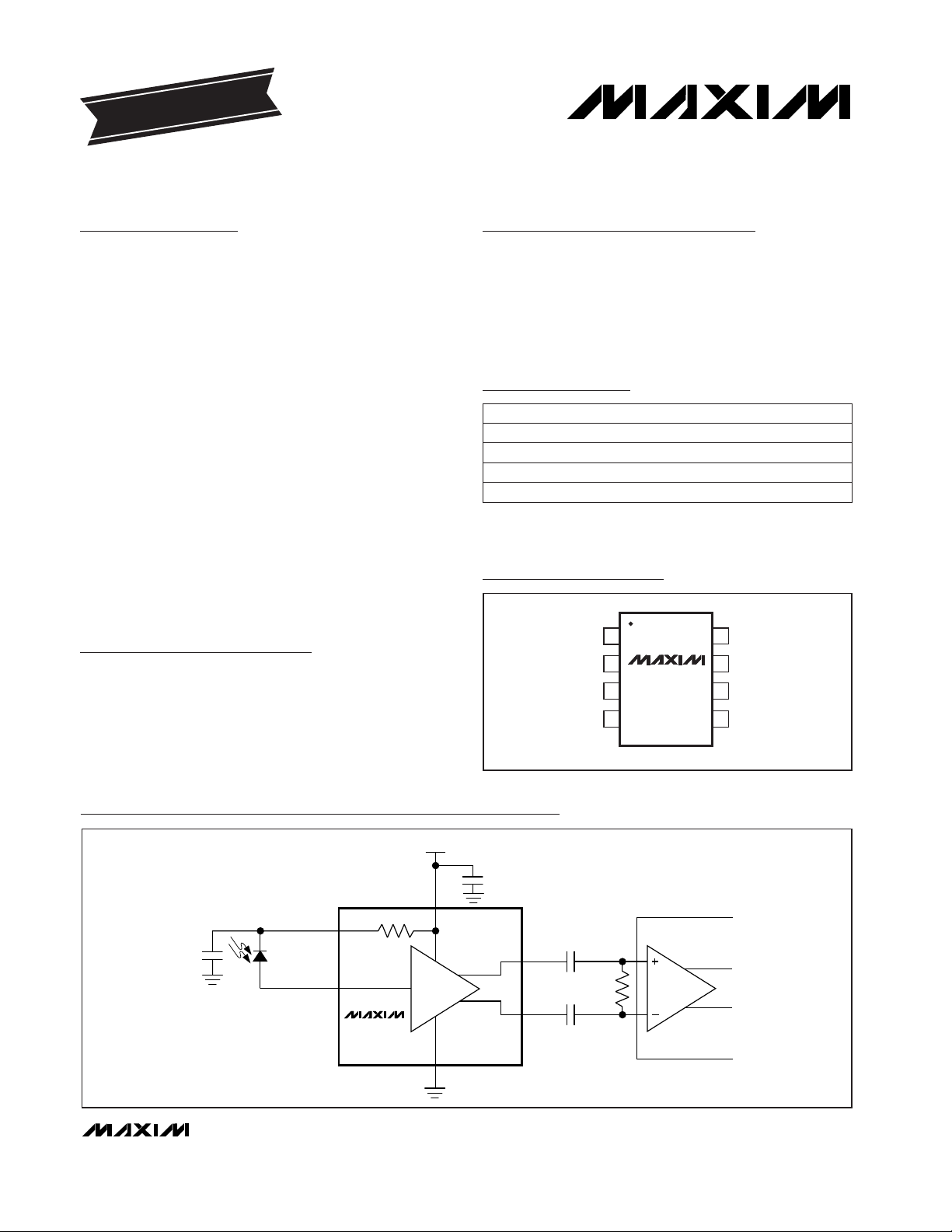
OUT-
GNDFILTER
1
2
87GND
OUT+N.C.
IN
V
CC
SO
TOP VIEW
3
4
6
5
MAX3266
MAX3267
0.01µF
PHOTODIODE
1.5k
V
CC
V
CC
GND
FILTER
IN
0.1µF
OUT+
OUT-
0.1µF
C
FILTER
400pF
100Ω
MAX3266
MAX3267
LIMITING
AMPLIFIER
Typical Application Circuit
19-4796; Rev 0; 1/99
PART
MAX3266CSA
MAX3266C/D —
0°C to +70°C
TEMP. RANGE PIN-PACKAGE
8 SO
Dice*
EVALUATION KIT
AVAILABLE
*
Dice are designed to operate with junction temperatures of 0°C
to +100°C but are tested and guaranteed only at TA= +25°C.
Pin Configuration
Ordering Information
MAX3267CSA
MAX3267C/D —
0°C to +70°C 8 SO
Dice*

ps
MAX3266/MAX3267
1.25Gbps/2.5Gbps, 3V to 5.5V, Low-Noise
Transimpedance Preamplifiers for LANs
2 _______________________________________________________________________________________
ABSOLUTE MAXIMUM RATINGS
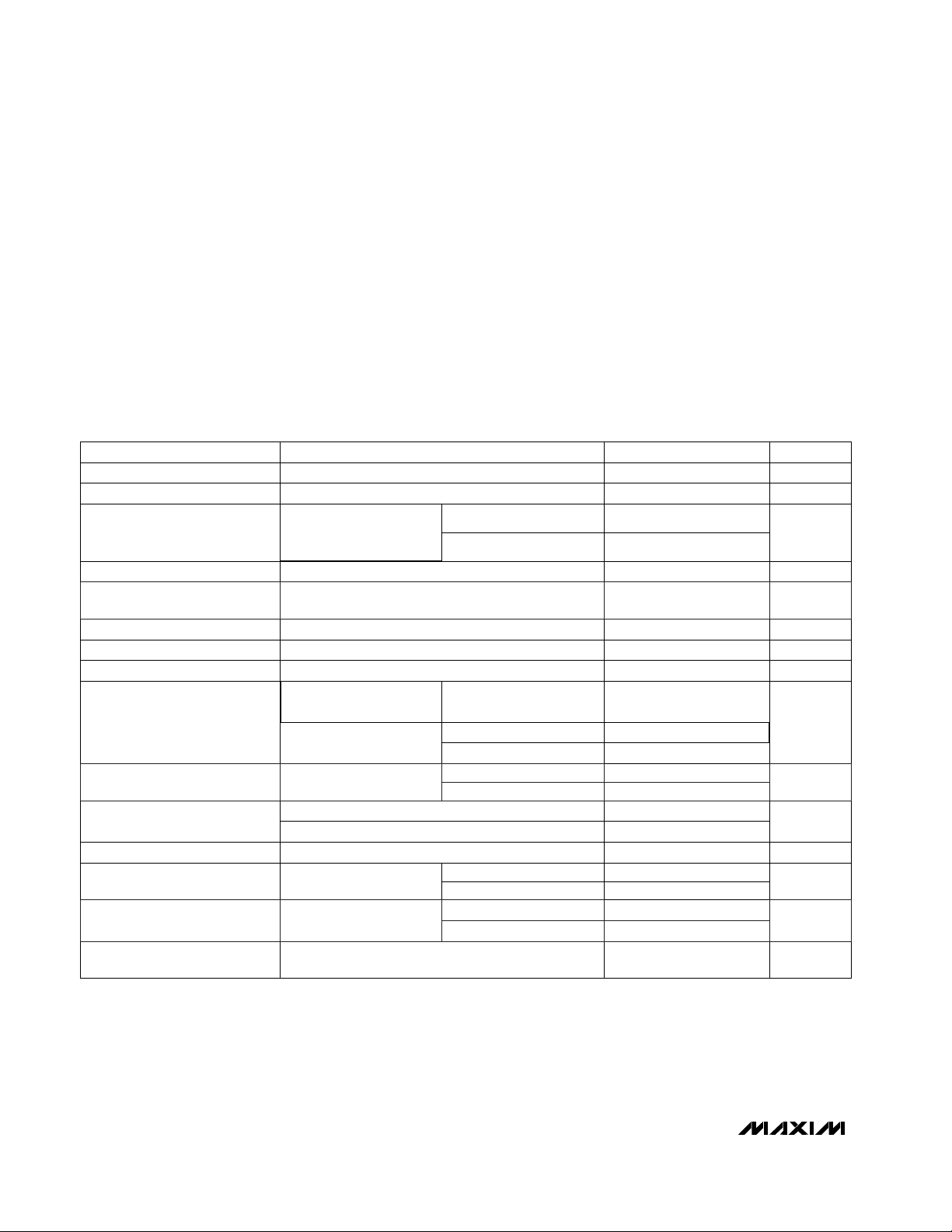
ELECTRICAL CHARACTERISTICS
(VCC= +3.0V to +5.5V, TA= 0°C to +70°C, 100Ω load between OUT+ and OUT-. Typical values are at TA = +25°C, V
CC
= 3.3V,
source capacitance = 0.85pF, unless otherwise noted.) (Note 1)
Stresses beyond those listed under “Absolute Maximum Ratings” may cause permanent damage to the device. These are stress ratings only, and functional
operation of the device at these or any other conditions beyond those indicated in the operational sections of the specifications is not implied. Exposure to
absolute maximum rating conditions for extended periods may affect device reliability.
Supply Voltage (V
CC
- GND).................................-0.5V to +6.0V
IN Current..............................................................-4mA to +4mA
FILTER Current......................................................-8mA to +8mA
Voltage at OUT+, OUT-...................(V
CC
- 1.5V) to (V
CC
+ 0.5V)
Continuous Power Dissipation (T
A
= +70°C)
SO package (derate 6.7mW/°C above +70°C).............533mW
Storage Temperature Range.............................-55°C to +150°C
Operating Junction Temperature (die)..............-55°C to +150°C
Processing Temperature (die).........................................+400°C
Lead Temperature (soldering, 10sec).............................+300°C
MAX3267
MAX3266
MAX3267
MAX3266
MAX3267
MAX3266
MAX3266
MAX3267
MAX3266
Power-Supply Rejection Ratio
(PSRR)
50 dB
Output referred, f < 2MHz
PSRR = -20log (∆V
OUT
/∆VCC)
19 76
Transimpedance Linear Range
40
µAp-p
30
Low-Frequency Cutoff 44 kHz
750 920 1100
Small-Signal Bandwidth
1530 1900 2420
MHz
Peak-to-peak
0.95 < linearity < 1.05
-3dB, input ≤ 20µADC
6.6
Input-Referred RMS Noise
485 655
nA
200
DC Input Overload
AC Input Overload 1.0 mAp-p
0.65 mA
192 256
SO package
(Note 2)
Die, packaged in TO-56
header (Note 2)
PARAMETER MIN TYP MAX UNITS
Filter Resistor 1220 1500 1860 Ω
Output Impedance 48 50 52 Ω
Transimpedance
1540 1900 2330
Ω
Supply Current
Input Bias Voltage 0.69 0.83 0.91 V
26 50 mA
2260 2800 3400
CONDITIONS
Single-ended (per side)
Differential, measured
with 30µAp-p signal
(40µAp-p for MAX3267)
Note 1: Source Capacitance represents the total capacitance at the IN pin during characterization of noise and bandwidth parame-
ters. Figure 1 shows the typical source capacitance vs. reverse voltage for the photodiode used during characterization of
TO-56 header packages. Noise and bandwidth will be affected by the source capacitance. See the
Typical Operating
Characteristics
for more information.
Note 2: Input-Referred Noise is calculated as RMS Output Noise / (Gain at f = 10MHz). Noise Density is (Input-Referred Noise) /
√
bandwidth. No external filters are used for the noise measurements.
Note 3: Deterministic Jitter is measured with the K28.5 pattern applied to the input [00111110101100000101].
Maximum Differential Output
Voltage
185 250 415 mVp-pInput = 1mAp-p
MAX3266
MAX3267
Input-Referred Noise Density
11.0
pA/(Hz)
1/2
(Note 2)
Deterministic Jitter
12 50
ps(Note 3)
MAX3266
MAX3267

MAX3266/MAX3267
1.25Gbps/2.5Gbps, 3V to 5.5V, Low-Noise
Transimpedance Preamplifiers for LANs
_______________________________________________________________________________________
3
170
180
190
200
210
220
230
240
250
0 255075100
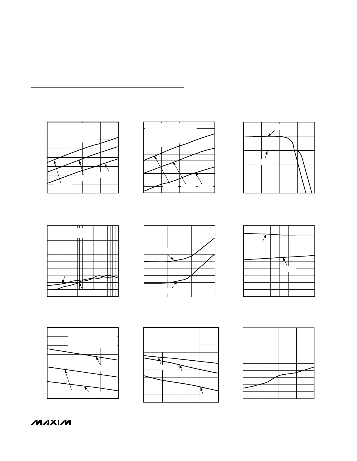
MAX3266
INPUT-REFERRED NOISE vs. TEMPERATURE
MAX3266/67-01
JUNCTION TEMPERATURE (°C)
INPUT-REFERRED NOISE (nA)
CIN = 1.5pF
CIN = 1.0pF
CIN = 0.5pF
CIN IS SOURCE CAPACITANCE
PRESENTED TO DIE, INCLUDES
PACKAGE PARASITIC, PIN DIODE,
AND PARASITIC INTERCONNECT
CAPACITANCE
420
440
460
480
500
520
540
560
580
600
620
640
0 255075100
MAX3267
INPUT-REFERRED NOISE vs. TEMPERATURE
MAX3267 toc02
JUNCTION TEMPERATURE (°C)
INPUT-REFERRED NOISE (nA)
CIN IS SOURCE CAPACITANCE
PRESENTED TO DIE, INCLUDES
PACKAGE PARASITIC, PIN DIODE,
AND PARASITIC INTERCONNECT
CAPACITANCE
CIN 1.5pF
CIN 1.0pF CIN 0.5pF
50
60
55
70
65
75
1M 10M 100M 1G 10G
FREQUENCY RESPONSE
MAX3266/67-03
FREQUENCY (Hz)
TRANSIMPEDANCE (dB)
MAX3267
MAX3266
100
0
10 100 1000
DETERMINISTIC JITTER
vs. INPUT AMPLITUDE
20
10
MAX3266/67-04
PEAK-TO-PEAK AMPLITUDE (µA)
PEAK-TO-PEAK JITTER (ps)
40
30
60
70
50
80
90
K28.5 DATA STREAM
EXTINCTION RATIO > 8
MAX3267
MAX3266
740
890
840
790
940
990
1040
1090
0 25 50 75 100
MAX3266
BANDWIDTH vs. TEMPERATURE
MAX3266/67-07
JUNCTION TEMPERATURE (°C)
BANDWIDTH (MHz)
CIN IS SOURCE CAPACITANCE
PRESENTED TO DIE, INCLUDES
PACKAGE PARASITIC, PIN DIODE,
AND PARASITIC INTERCONNECT
CAPACITANCE
CIN = 1.5pF
CIN = 1.0pF
CIN = 0.5pF
0
300
200
100
400
500
600
700
800
900
1000
1 10 100 1000
INPUT-REFERRED RMS NOISE CURRENT
vs. DC INPUT CURRENT
MAX3266/67-05
DIFFERENTIAL DC INPUT CURRENT (µA)
INPUT-REFERRED NOISE (nA)
MAX3267
MAX3266
60
63
62
61
64
65
66
67
68
69
70
01020304050607080
SMALL-SIGNAL TRANSIMPEDANCE
vs. TEMPERATURE
MAX3266/67-06
AMBIENT TEMPERATURE (°C)
TRANSIMPEDANCE (dB)
MAX3267
MAX3266
200
260
240
220
280
300
320
340
360
380
400
020406080
MAX3266/MAX3267
OUTPUT AMPLITUDE vs. TEMPERATURE
MAX3266/67-08
AMBIENT TEMPERATURE (°C)
AMPLITUDE (mV)
INPUT = 1mAp-p
Typical Operating Characteristics
(VCC= +3.3V, TA= +25°C, MAX3266/MAX3267 EV kit, source capacitance = 0.85pF, unless otherwise noted.)
1500
1700
1800
1900
2000
2100
2200
2300
2400
0 25 50 75 100
MAX3267
BANDWIDTH vs. TEMPERATURE
MAX3367 toc3
JUNCTION TEMPERATURE (°C)
BANDWIDTH (MHz)
1600
CIN IS SOURCE CAPACITANCE
PRESENTED TO DIE, INCLUDES
PACKAGE PARASITIC, PIN DIODE,
AND PARASITIC INTERCONNECT
CAPACITANCE
C
IN
= 1.5pF
C
IN
= 0.5pF
C
IN
= 1.0pF
 Loading...