Maxim MAX3264C Datasheet
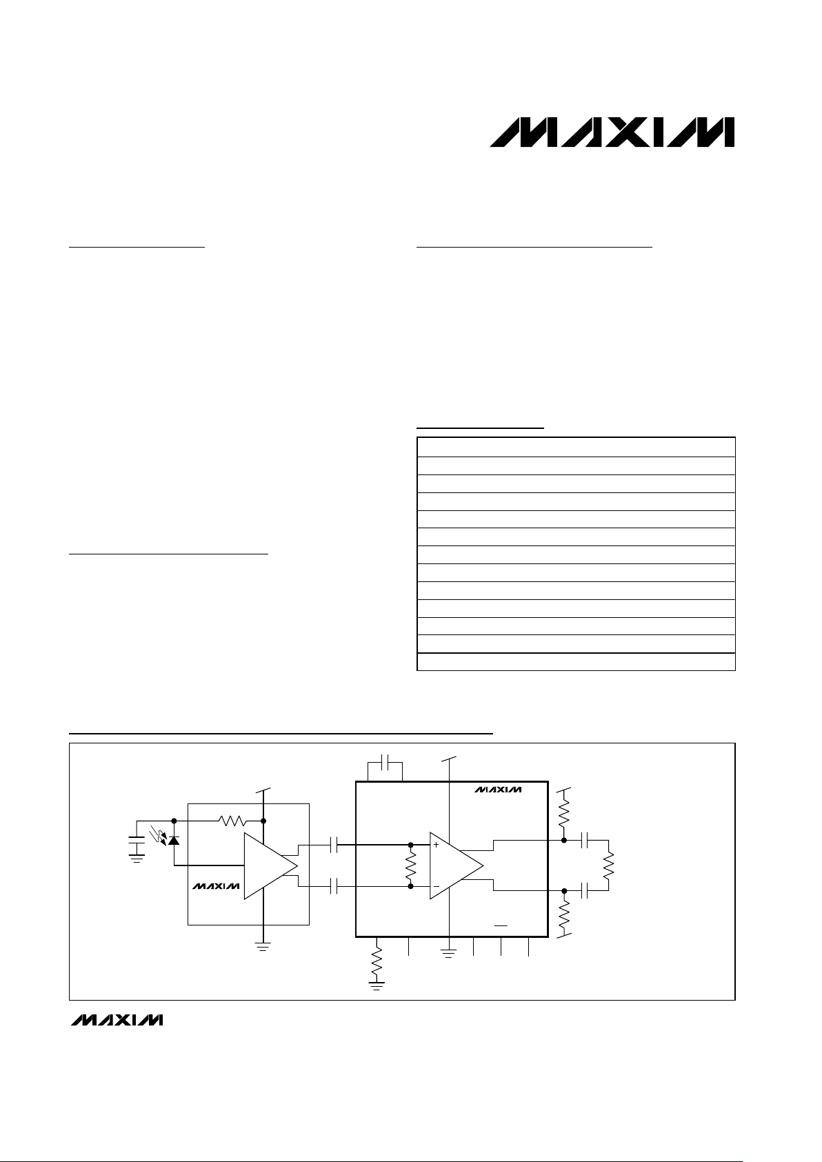
V
CC
V
CC
C
AZ
CAZ1 CAZ2
V
CC
V
CC
C
IN
0.01µF
0.01µF
0.01µF
C
IN
0.01µF
TH SQUELCH
N.C.
100Ω
IN-
IN+
OUT+
R
TERM
R
TERM
R
L
100Ω
OUT-
MAX3266
MAX3267
MAX3264CUE
MAX3265CUE
MAX3265EUE
LOS
LOSS
OF
SIGNAL
LOS
N.C.
R
TH
LEVEL
N.C.
General Description
The 1.25Gbps MAX3264/MAX3268/MAX3768 and the
2.5Gbps MAX3265/MAX3269/MAX3765 limiting amplifiers are designed for Gigabit Ethernet and Fibre
Channel optical receiver systems. The amplifiers accept
a wide range of input voltages and provide constantlevel output voltages with controlled edge speeds.
Additional features include RMS power detectors with
programmable loss-of-signal (LOS) indication, an
optional squelch function that mutes the data output signal when the input voltage falls below a programmable
threshold, and excellent jitter performance.
The MAX3264/MAX3265/MAX3765 feature current-mode
logic (CML) data outputs that are tolerant of inductive
connectors and a 16-pin TSSOP package, making these
circuits ideal for GBIC receivers. The MAX3268/
MAX3269/MAX3768 feature standards-compliant positive-referenced emitter-coupled logic (PECL) data outputs and are available in a tiny 10-pin µMAX package
that is ideal for small-form-factor (SFF) receivers.
Applications
Gigabit Ethernet Optical Receivers
Fibre Channel Optical Receivers
System Interconnect
ATM Optical Receivers
Features
♦ +3.0V to +5.5V Supply Voltage
♦ Low Deterministic Jitter
14ps (MAX3264)
11ps (MAX3265/MAX3765)
♦ 150ps (max) Edge Speed (MAX3265/MAX3765)
300ps (max) Edge Speed (MAX3264)
♦ Programmable Signal-Detect Function
♦ Choice of CML or PECL Output Interface
♦ 10-Pin µMAX or 16-Pin TSSOP Package
MAX3264/MAX3265/MAX3268/MAX3269/MAX3765/MAX3768
+3.0V to +5.5V, 1.25Gbps/2.5Gbps
Limiting Amplifiers
________________________________________________________________ Maxim Integrated Products 1
19-1523; Rev 5, 7/03
*Dice are designed to operate from 0°C to +70°C, but are tested
and guaranteed only at TA= +25°C.
†
EP = Exposed paddle.
Ordering Information
Selector Guide appears at end of data sheet.
Pin Configurations appear at end of data sheet.
Typical Operating Circuits
Typical Operating Circuits continued at end of data sheet.
For pricing, delivery, and ordering information, please contact Maxim/Dallas Direct! at
1-888-629-4642, or visit Maxim’s website at www.maxim-ic.com.
PART TEMP RANGE PIN-PACKAGE
MAX3264CUE 0°C to +70°C 16 TSSOP-EP
†
MAX3264C/D 0°C to +70°C Dice*
MAX3265CUE 0°C to +70°C 16 TSSOP-EP
†
MAX3265CUB 0°C to +70°C 10 µMAX-EP
†
MAX3265C/D 0°C to +70°C Dice*
MAX3265EUE -40°C to +85°C 16 TSSOP-EP
†
MAX3268CUB 0°C to +70°C 10 µMAX-EP
†
MAX3268C/D 0°C to +70°C Dice*
MAX3269CUB 0°C to +70°C 10 µMAX-EP
†
MAX3269C/D 0°C to +70°C Dice*
MAX3765CUB 0°C to +70°C 10 µMAX-EP
†
MAX3768CUB 0°C to +70°C 10 µMAX-EP
†
MAX3264/MAX3265/MAX3268/MAX3269/MAX3765/MAX3768
+3.0V to +5.5V, 1.25Gbps/2.5Gbps
Limiting Amplifiers
2 _______________________________________________________________________________________
ABSOLUTE MAXIMUM RATINGS
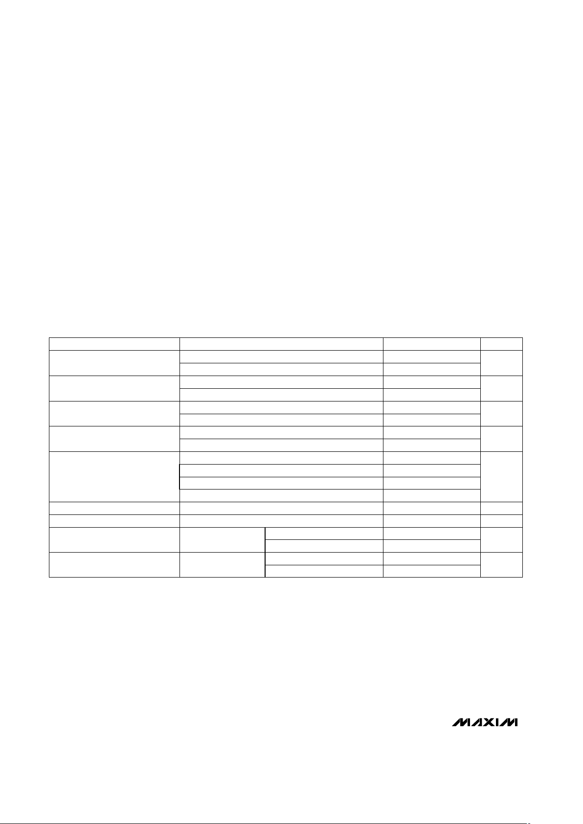
ELECTRICAL CHARACTERISTICS
(Data outputs terminated per Figure 1, VCC= +3.0V to +5.5V, TA= 0°C to +70°C. Typical values are at V
CC
= +3.3V, TA= +25°C,
unless otherwise noted.) (Note 1)
Stresses beyond those listed under “Absolute Maximum Ratings” may cause permanent damage to the device. These are stress ratings only, and functional
operation of the device at these or any other conditions beyond those indicated in the operational sections of the specifications is not implied. Exposure to
absolute maximum rating conditions for extended periods may affect device reliability.
Supply Voltage (VCC) ............................................-0.5V to +6.0V
Voltage at IN+, IN- ..........................(V
CC
- 2.4V) to (VCC+ 0.5V)
Voltage at SQUELCH, CAZ1,
CAZ2, LOS, LOS, TH..................................-0.5V to (V
CC
+ 0.5V)
Voltage at LEVEL...................................................-0.5V to +2.0V
Current into LOS, LOS ..........................................-1mA to +9mA
Differential Input Voltage (IN+ - IN-) .....................................2.5V
Continuous Current at
CML Outputs (OUT+, OUT-) ..........................-25mA to +25mA
Continuous Current at PECL Outputs (OUT+, OUT-) .........50mA
Continuous Power Dissipation (T
A
= +70°C)
16-Pin TSSOP (derate 27mW/°C above +70°C) .........2162mW
10-Pin µMAX (derate 20mW/°C above +70°C) ...........1600mW
Operating Ambient Temperature Range .............-40°C to +85°C
Storage Temperature Range .............................-55°C to +150°C
Processing Temperature (dice) .......................................+400°C
Lead Temperature (soldering, 10s) .................................+300°C
Deterministic Jitter
MAX3265/MAX3269/MAX3765 (Notes 2, 3)
MAX3265/MAX3269/MAX3765
MAX3264/MAX3268/MAX3768
MAX3265/MAX3269/MAX3765
MAX3264/MAX3268/MAX3768
4.5
8.5
Low LOS Deassert Level mVRTH= 2.5kΩ
MAX3264/MAX3268/MAX3768 (Notes 2, 3)
PARAMETER MIN TYP MAX UNITS
10 1200
5 1200
Data Rate Gbps
Input Voltage Range mV
14 30
11 25
1.25
2.5
psp-p
15
Random Jitter
8
ps
RMS
80 175 300
100 150
80 150 300
Data Output Edge Speed
100 150
ps
LOS Hysteresis 2.5 4.4 dB
LOS Assert/Deassert Time 1 µs
1.20 2.6
2.20 4.8
Low LOS Assert Level mV
CONDITIONS
MAX3264/MAX3268/MAX3768 (Notes 2, 4)
MAX3265/MAX3269/MAX3765
MAX3264/MAX3268/MAX3768
MAX3265/MAX3269/MAX3765 (Notes 2, 4)
MAX3264 (Note 5)
MAX3265/MAX3765 (Note 6)
MAX3268/MAX3768 (Note 5)
MAX3269 (Note 6)
MAX3264/MAX3268/MAX3768
(Notes 2, 7)
MAX3265/MAX3269/MAX3765
(Notes 7, 8)
RTH= 2.5kΩ
MAX3264/MAX3265/MAX3268/MAX3269/MAX3765/MAX3768
+3.0V to +5.5V, 1.25Gbps/2.5Gbps
Limiting Amplifiers
_______________________________________________________________________________________ 3
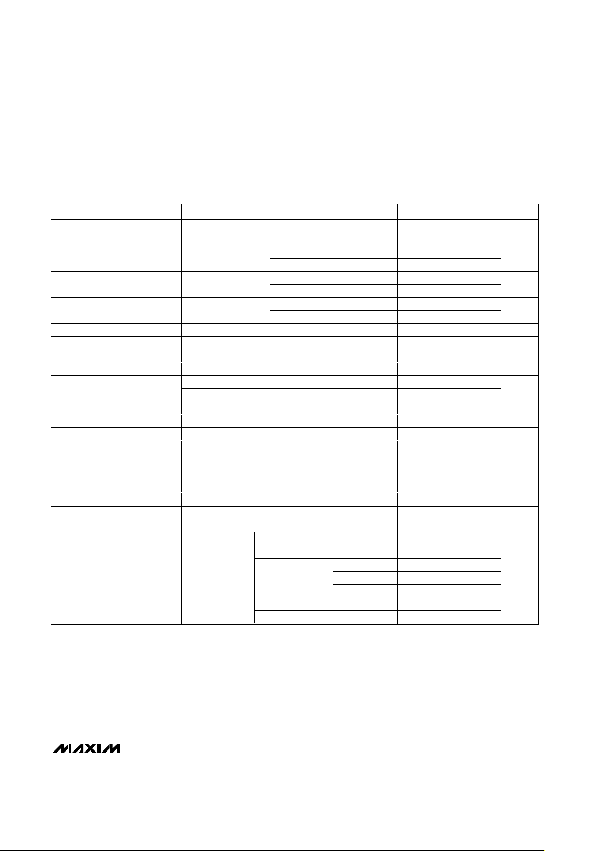
ELECTRICAL CHARACTERISTICS (continued)
(Data outputs terminated per Figure 1, VCC= +3.0V to +5.5V, TA= 0°C to +70°C. Typical values are at V
CC
= +3.3V, TA= +25°C,
unless otherwise noted.) (Note 1)
PARAMETER CONDITIONS MIN TYP MAX UNITS
MAX3264/MAX3268/MAX3768 5.6 9
Medium LOS Assert Level RTH = 7kΩ
MAX3265/MAX3269/MAX3765
9.9 16
mV
MAX3264/MAX3268/MAX3768
15 19.8
Medium LOS Deassert Level RTH = 7kΩ
MAX3265/MAX3269/MAX3765
27 40.5
mV
MAX3264/MAX3268/MAX3768 9.4 21.6
High LOS Assert Level RTH = 20kΩ
MAX3265/MAX3269/MAX3765 18.0 41.5
mV
MAX3264/MAX3268/MAX3768 35
High LOS Deassert Level RTH = 20kΩ
MAX3265/MAX3269/MAX3765 67
mV
Squelch Input Current 0 80 400 µA
Differential Input Resistance IN+ to IN- 97 100 103 Ω
MAX3264/MAX3268/MAX3768 150
Input-Referred Noise
MAX3265/MAX3269/MAX3765 230
µV
RMS
LEVEL = open, R
LOAD
= 50Ω 550 1200
CML Output Voltage
LEVEL = GND, R
LOAD
= 75Ω 1100 1270 1800
mV
PECL Output High Voltage
Referenced to V
CC
-1.025 -0.880 V
PECL Output Low Voltage
Referenced to V
CC
-1.810 +1.620 V
LOS Output High Voltage
I
LOS
= -30µA 2.4 V
LOS Output Low Voltage
I
LOS
= +1.2mA 0.4 V
Output Signal When Squelched
Outputs AC-coupled 20 mV
Power-Supply Rejection Ratio
f < 2MHz 20 dB
CAZ = open 2 MHz
Low-Frequency Cutoff
C
AZ
= 0.1µF 2 kHz
MAX3264/MAX3265/MAX3765 85 100 115
O utp ut Resi stance ( S i ng l e E nd ed )
MAX3268/MAX3269/MAX3768 4
Ω
MAX3268 39 62
MAX3269 48 78
MAX3264 38 62
MAX3265 50 76
MAX3765 50 76
Output not
squelched
MAX3768 39 62
Power-Supply Current Figure 2
Output squelched MAX3765 64 90
mA
mV
V
V
mV
MAX3264/MAX3265/MAX3268/MAX3269/MAX3765/MAX3768
+3.0V to +5.5V, 1.25Gbps/2.5Gbps
Limiting Amplifiers
4 _______________________________________________________________________________________
Note 1: Specifications for Input Voltage Range, LOS Assert/Deassert Levels, and CML Output Voltage refer to the total differential
peak-to-peak signal applied or measured. PECL output voltages are absolute (single-ended) voltages measured at a single
output.
Note 2: Input edge speed is controlled using four-pole, lowpass Bessel filters with bandwidth approximately 75% of the maximum
data rate.
Note 3: Deterministic jitter is measured with a K28.5 pattern (0011 1110 1011 0000 0101). Deterministic jitter is the peak-to-peak
deviation from ideal time crossings, measured at the zero-level crossings of the differential output per ANSI X3.230,
Annex A.
Note 4: Random jitter is measured with the minimum input signal applied after filtering with a four-pole, lowpass, Bessel filter (fre-
quency bandwidth at 75% of the maximum data rate). For Fibre Channel and Gigabit Ethernet applications, the peak-topeak random jitter is 14.1-times the RMS random jitter.
Note 5: Input signal applied after a 933MHz Bessel filter.
Note 6: Input signal applied after a 1.8GHz Bessel filter.
Note 7: Input for LOS assert/deassert and hysteresis tests is a repeating K28.5 pattern. Hysteresis is defined as:
20log (V
LOS-DEASSERT
/ V
LOS-ASSERT
).
Note 8: Response time to a 10dB change in input power.
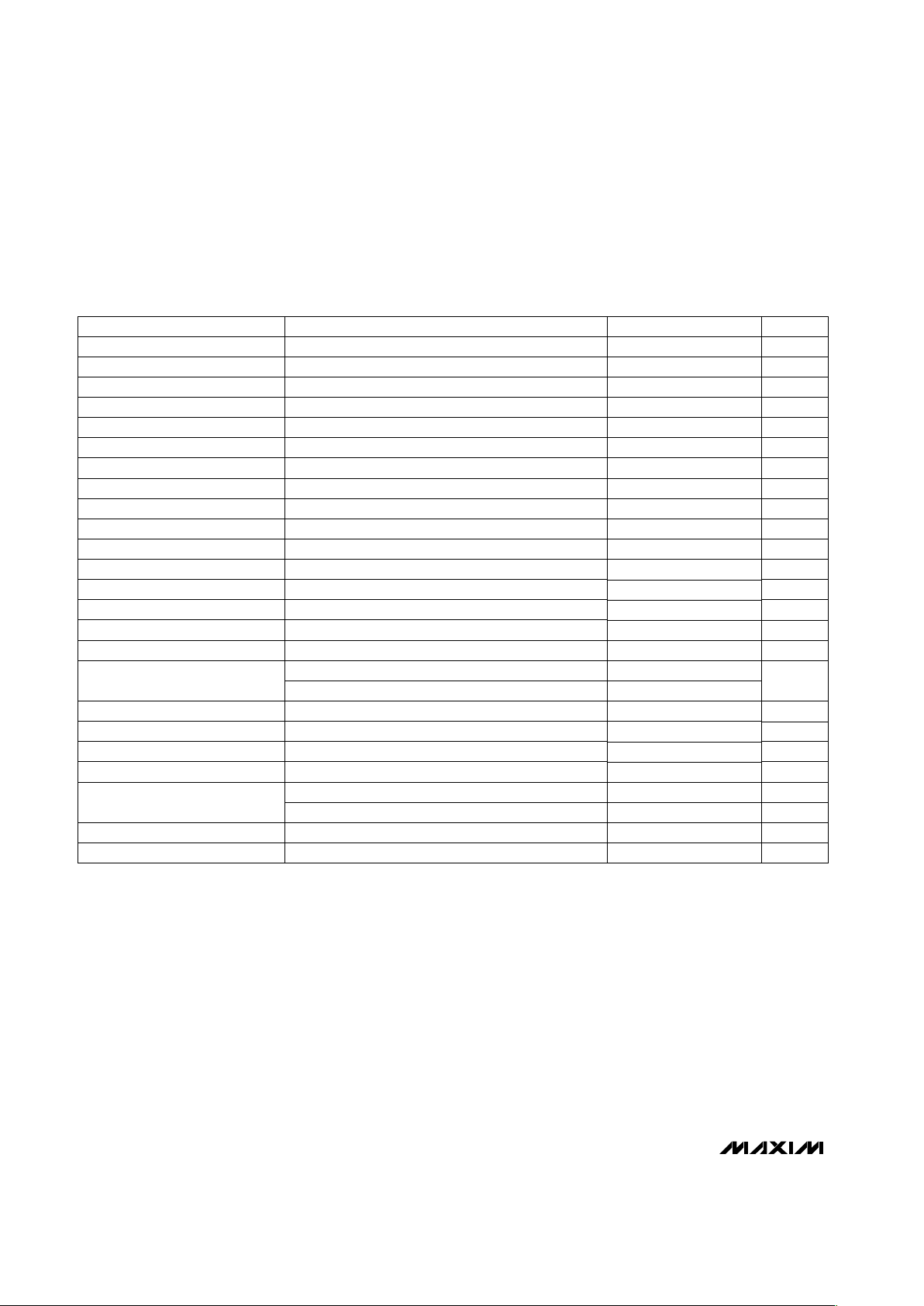
ELECTRICAL CHARACTERISTICS—MAX3265EUE
(Data outputs terminated per Figure 1, VCC= +3.0V to +5.5V, TA= -40°C to +85°C. Typical values are at V
CC
= +3.3V, TA= +25°C,
unless otherwise noted.) (Note 1)
CONDITIONS
Data Rate Gbps
2.5
UNITSMIN TYP MAXPARAMETER
Input Voltage Range mV
10 1200
(Notes 2, 3)Deterministic Jitter ps
p-p
11 25
(Notes 2, 4)Random Jitter ps
RMS
8
(Note 6)Data Output Edge Speed ps
100 155
(Notes 2, 7)LOS Hysteresis dB
2.2 4.4
(Notes 7, 8)LOS Assert/Deassert Time µs
1
Output Resistance (single ended) Ω
85 100 115
CAZ= 0.1µF kHz
2
CAZ= open
Low-Frequency Cutoff
MHz
2
f < 2MHzPower-Supply Rejection Ratio dB
20
Outputs AC-coupledOutput Signal When Squelched
20
I
LOS
= +1.2mALOS Output Low Voltage
0.450
I
LOS
= -30µALOS Output High Voltage
LEVEL = GND, R
LOAD
= 75Ω
1100 1270 1800
LEVEL = open, R
LOAD
= 50Ω
CML Output Voltage
550 1200
Input-Referred Noise
µV
RMS
230
IN+ to IN-Differential Input Resistance
Ω
97 100 103
Squelch Input Current
µA
0 80 400
RTH= 20kΩHigh LOS Deassert Level mV
67 111
RTH= 20kΩHigh LOS Assert Level mV
18.0 41.5
RTH= 7kΩMedium LOS Deassert Level mV
27 43.0
RTH= 7kΩMedium LOS Assert Level mV
9.9 16
RTH= 2.5kΩLow LOS Deassert Level mV
8.5 13.6
RTH= 2.5kΩLow LOS Assert Level mV
2.20 4.8
Figure 2Power-Supply Current mA
50 76
2.4
MAX3264/MAX3265/MAX3268/MAX3269/MAX3765/MAX3768
+3.0V to +5.5V, 1.25Gbps/2.5Gbps
Limiting Amplifiers
_______________________________________________________________________________________ 5
0
25
20
15
10
5
30
0 200 400 600 800 1000 1200
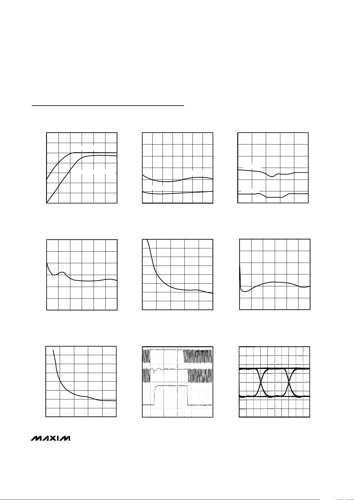
MAX3264/MAX3268/MAX3768
DETERMINISTIC JITTER
vs. INPUT AMPLITUDE
MAX3264/5/8/9 TOC04
INPUT AMPLITUDE (mV)
JITTER (ps)
0
14
12
10
8
6
2
4
16
0 1020304050
MAX3264/MAX3268/MAX3768
RANDOM JITTER
vs. INPUT AMPLITUDE
MAX3264/5/8/9 TOC05
INPUT AMPLITUDE (mV)
RMS JITTER (ps)
300
900
700
500
1300
1100
1500
1700
024681012
OUTPUT VOLTAGE
vs. INPUT VOLTAGE
MAX3264/5/8/9 TOC01a
INPUT VOLTAGE (mV)
OUTPUT VOLTAGE (mV)
MAX3264/MAX3268
MAX3265/MAX3269/MAX3765
3.5
4.0
6.5
6.0
5.5
5.0
4.5
0 10203040506070
MAX3264
LOS HYSTERESIS vs. TEMPERATURE
MAX3264/5/8/9 TOC03a
TEMPERATURE (°C)
LOS HYSTERESIS (dB)
RTH = 25kΩ
RTH = 7kΩ
0
25
20
15
10
5
30
0 200 400 600 800 1000 1200
MAX3265/MAX3269/MAX3765
DETERMINISTIC JITTER
vs. INPUT AMPLITUDE
MAX3264/5/8/9 TOC06
INPUT AMPLITUDE (mV)
JITTER (ps)
0
7
6
5
4
3
1
2
8
0 1020304050
MAX3265/MAX3269/MAX3765
RANDOM JITTER
vs. INPUT AMPLITUDE
MAX3264/5/8/9 TOC07
INPUT AMPLITUDE (mV)
RMS JITTER (ps)
V
IN
V
OUT
V
LOS
LOSS OF SIGNAL WITH SQUELCH
MAX3264/5/8/9 TOC08
500ns/div
300mV/div
200ps/div
MAX3268/MAX3768
DATA OUTPUT EYE DIAGRAM
(MINIMUM INPUT)
MAX3264/5/8/9 TOC09
Typical Operating Characteristics
(TA = +25°C, unless otherwise noted.)
3.5
4.0
6.5
6.0
5.5
5.0
4.5
-40 -15 10 35 60 85
MAX3265EUE
LOS HYSTERESIS vs. TEMPERATURE
MAX3264/5/8/9 TOC03
TEMPERATURE (°C)
LOS HYSTERESIS (dB)
RTH = 4.6kΩ
RTH = 16kΩ
MAX3264/MAX3265/MAX3268/MAX3269/MAX3765/MAX3768
+3.0V to +5.5V, 1.25Gbps/2.5Gbps
Limiting Amplifiers
6 _______________________________________________________________________________________
Typical Operating Characteristics (continued)
(TA = +25°C, unless otherwise noted.)
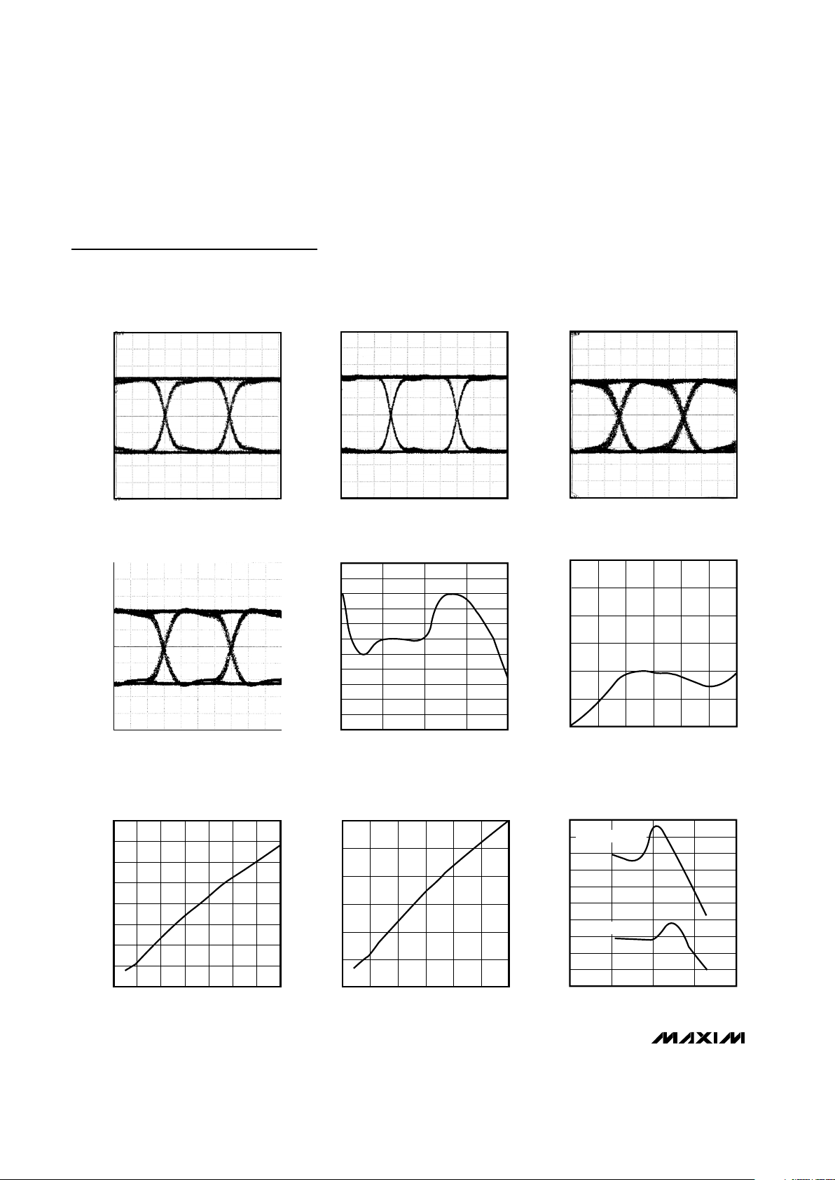
150mV/div
MAX3265/MAX3765
DATA OUTPUT EYE DIAGRAM
2.5Gbps (MAXIMUM INPUT)
MAX3264/5/8/9 TOC13
100ps/div
0
25
15
20
10
5
100k 1M 10M 100M 1G
POWER-SUPPLY REJECTION RATIO
vs. FREQUENCY
MAX3264/5/8/9 TOC14
FREQUENCY (Hz)
PSRR (dB)
1.0
3.5
3.0
2.5
1.5
2.0
4.0
0 0.5 1.0 1.5 2.0 3.0
OUTPUT VSWR vs. FREQUENCY
MAX3264/5/8/9 TOC15
FREQUENCY (GHz)
VSWR
2.5
0
10
5
20
15
35
30
25
40
0105 1520253035
MAX3264
LOSS-OF-SIGNAL THRESHOLD vs. R
TH
MAX3264/5/8/9 TOC18
RTH (kΩ)
LOS ASSERT THRESHOLD (mV)
0
50
40
30
10
20
60
010203051525
MAX3265/MAX3765
LOSS-OF-SIGNAL THRESHOLD vs. R
TH
MAX3264/5/8/9 TOC19
RTH (kΩ)
LOS ASSERT THRESHOLD (mV)
5
40
45
50
35
30
20
15
10
25
55
1M 100M 10G10M 1G
COMMON-MODE REJECTION RATIO
vs. FREQUENCY
MAX3264/5/8/9 TOC20
FREQUENCY (Hz)
CMRR (dB)
MAX3268/MAX3768
MAX3265/MAX3765
150mV/div
MAX3264
DATA OUTPUT EYE DIAGRAM AT
1.25Gbps (MINIMUM INPUT)
MAX3264/5/8/9 TOC10
200ps/div
50mV/div
MAX3264
DATA OUTPUT EYE DIAGRAM AT
1.25Gbps (MAXIMUM INPUT)
MAX3264/5/8/9 TOC11
200ps/div
150mV/div
MAX3265/MAX3765
DATA OUTPUT EYE DIAGRAM
2.5Gbps (MINIMUM INPUT)
MAX3264/5/8/9 TOC12
100ps/div
 Loading...