Maxim MAX3263CAG Datasheet

________________General Description
The MAX3263 is a complete, easy-to-program, single
+5V-powered, 155Mbps laser diode driver with complementary enable inputs and automatic power control
(APC). The MAX3263 accepts differential PECL inputs
and provides complementary output currents. A temperature-stabilized reference voltage is provided to
simplify laser current programming. This allows modulation current to be programmed up to 30mA and bias
current to be programmed from up to 60mA with two
external resistors.
An APC circuit is provided to maintain constant laser
power in transmitters that use a monitor photodiode.
Only two external resistors are required to implement
the APC function.
The MAX3263’s fully integrated feature set includes a
TTL-compatible laser failure indicator and a programmable slow-start circuit to prevent laser damage. The
slow-start is preset to 50ns and can be extended by
adding an external capacitor.
________________________Applications
Laser Diode Transmitters
155Mbps SDH/SONET
155Mbps ATM
____________________________Features
♦ Rise Times Less than 1ns
♦ Differential PECL Inputs
♦ Single +5V Supply
♦ Automatic Power Control
♦ Temperature-Compensated Reference Voltage
♦ Complementary Enable Inputs
_______________Ordering Information
MAX3263
Single +5V, Fully Integrated,
155Mbps Laser Diode Driver
________________________________________________________________
Maxim Integrated Products
1
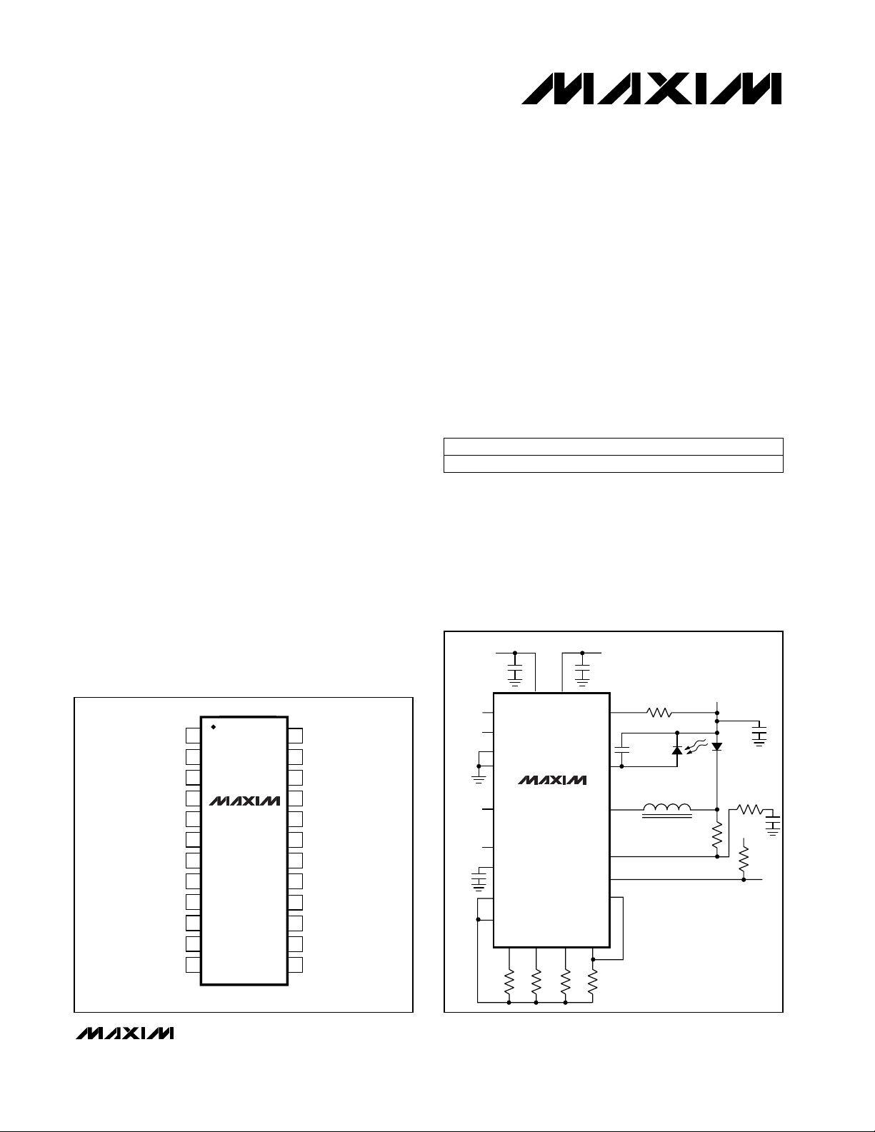
___________________Pin Configuration
19-0432; Rev 1b; 4/98
PART
MAX3263CAG 0°C to +70°C
TEMP. RANGE PIN-PACKAGE
24 SSOP
MAX3263
+5V
0.01µF 0.01µF
+5V
+5V
+5V
OUT+
IBIASOUT
IPIN
PECL
INPUTS
OUT-
FAILOUT
IBIASFB
OSADJ
IMODSET
IPINSET
IBIASSET
VCCA VCCB
VIN+
VIN-
ENB+
GNDB
GNDA
ENB-
SLWSTRT
VREF1
VREF2
LASER
2.7k
PHOTO-
DIODE
FERRITE BEAD
_____________Typical Operating Circuit
For free samples & the latest literature: http://www.maxim-ic.com, or phone 1-800-998-8800.
For small orders, phone 1-800-835-8769.
TOP VIEW
VREF2
1
IPINSET
2
FAILOUT
3
GNDB
4
VIN+
VIN-
GNDB
VCCB
ENB-
ENB+
VREF1
OSADJ
MAX3263
5
6
7
8
9
10
11
12
SSOP
24
23
22
21
20
19
18
17
16
15
14
13
SLWSTRT
IPIN
VCCA
GNDA
OUT+
GNDA
OUT-
GNDA
IBIASOUT
IMODSET
IBIASSET
IBIASFB

MAX3263
Single +5V, Fully Integrated,
155Mbps Laser Diode Driver
2 _______________________________________________________________________________________
Stresses beyond those listed under “Absolute Maximum Ratings” may cause permanent damage to the device. These are stress ratings only, and functional
operation of the device at these or any other conditions beyond those indicated in the operational sections of the specifications is not implied. Exposure to
absolute maximum rating conditions for extended periods may affect device reliability.
TA = +25°C
(Note 1)
CONDITIONS
mA12I
REF
Available Reference Current
V3.15 3.3 3.45V
REF
mA60I
BIAS
Range of Programmable Laser
Bias Current
Reference Voltage
VV
IL
TTL Low Input
mA50I
VCC
Supply Current
VVCC- 1.165V
IH
PECL Input High
VVCC- 1.475V
IL
PECL Input Low
V2 0.8V
IH
TTL High Input
UNITSMIN TYP MAXSYMBOLPARAMETER
Minimum differential input swing is 1100mVp-p
(Note 3)
CONDITIONS
mA30I
MOD
Range of Programmable
Modulation Current
UNITSMIN TYP MAXSYMBOLPARAMETER
I
BIAS
= 25mA, I
MOD
= 12mA, 4ns unit interval;
measured from 10% to 90%
ns1tR, t
F
Modulation-Current Rise and
Fall Time
I
MOD
= 12mA, TA= +25°C %±15OS
Aberrations, Rising and Falling
Edge
I
BIAS
= 25mA, I
MOD
= 12mA, 8ns period ps100PWD
Modulation-Current PulseWidth Distortion
ABSOLUTE MAXIMUM RATINGS
Terminal Voltage (with respect to GND)
Supply Voltages (V
CC
A, VCCB).............................-0.3V to +6V
VIN+, VIN-, FAILOUT ................................................0V to V
CC
OUT+, OUT-, IBIASOUT ......................................+1.5V to V
CC
ENB+, ENB- ......................VCCor +5.5V, whichever is smaller
Differential Input Voltage (
|
VIN+ - VIN-|).........................+3.8V
Input Current
IBIASOUT ............................................................0mA to 75mA
OUT+, OUT- ........................................................0mA to 40mA
IBIASSET ........................................................0mA to 1.875mA
IMODSET...............................................................0mA to 2mA
IPIN, IPINSET, OSADJ...........................................0mA to 2mA
FAILOUT..............................................................0mA to 10mA
IBIASFB................................................................-2mA to 2mA
Output Current
VREF1, VREF2.....................................................0mA to 20mA
SLWSTRT ..............................................................0mA to 5mA
Continuous Power Dissipation (T
A
= +70°C)
SSOP (derate 8mW/°C above +70°C) ..........................640mW
Operating Temperature Range...............................0°C to +70°C
Junction Temperature......................................................+150°C
Storage Temperature Range .............................-55°C to +175°C
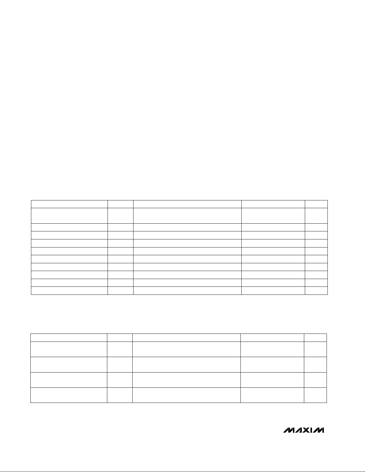
DC ELECTRICAL CHARACTERISTICS
(VCC= VCCA = VCCB = +4.75V to +5.25V, TA= 0°C to +70°C, unless otherwise noted. Typical values are at VCC= +5V and
TA= +25°C.)
AC ELECTRICAL CHARACTERISTICS
(VCC= VCCA = VCCB = +4.75V to +5.25V, R
LOAD
(at OUT+ and OUT-) = 25Ω connected to V
CC
, TA= 0°C to +70°C, unless other-
wise noted. Typical values are at VCC= +5V and TA= +25°C.) (Note 2)
Loaded with 2.7kΩ pull-up resistor to V
CC
Loaded with 2.7kΩ pull-up resistor to V
CC
V0.5V
OL
FAILOUT Output Low
V4.5V
OH
FAILOUT Output High
Note 2: AC characteristics are guaranteed by design and characterization.
Note 3: An 1100mVp-p differential is equivalent to complementary 550mVp-p signals on VIN+ and VIN-.
Note 1: I
VCC
= I
VCCA
+ I
VCCB
, I
BIAS
= 60mA, I
MOD
= 30mA, and I
PIN
= 140µA.

MAX3263
Single +5V, Fully Integrated,
155Mbps Laser Diode Driver
_______________________________________________________________________________________
3
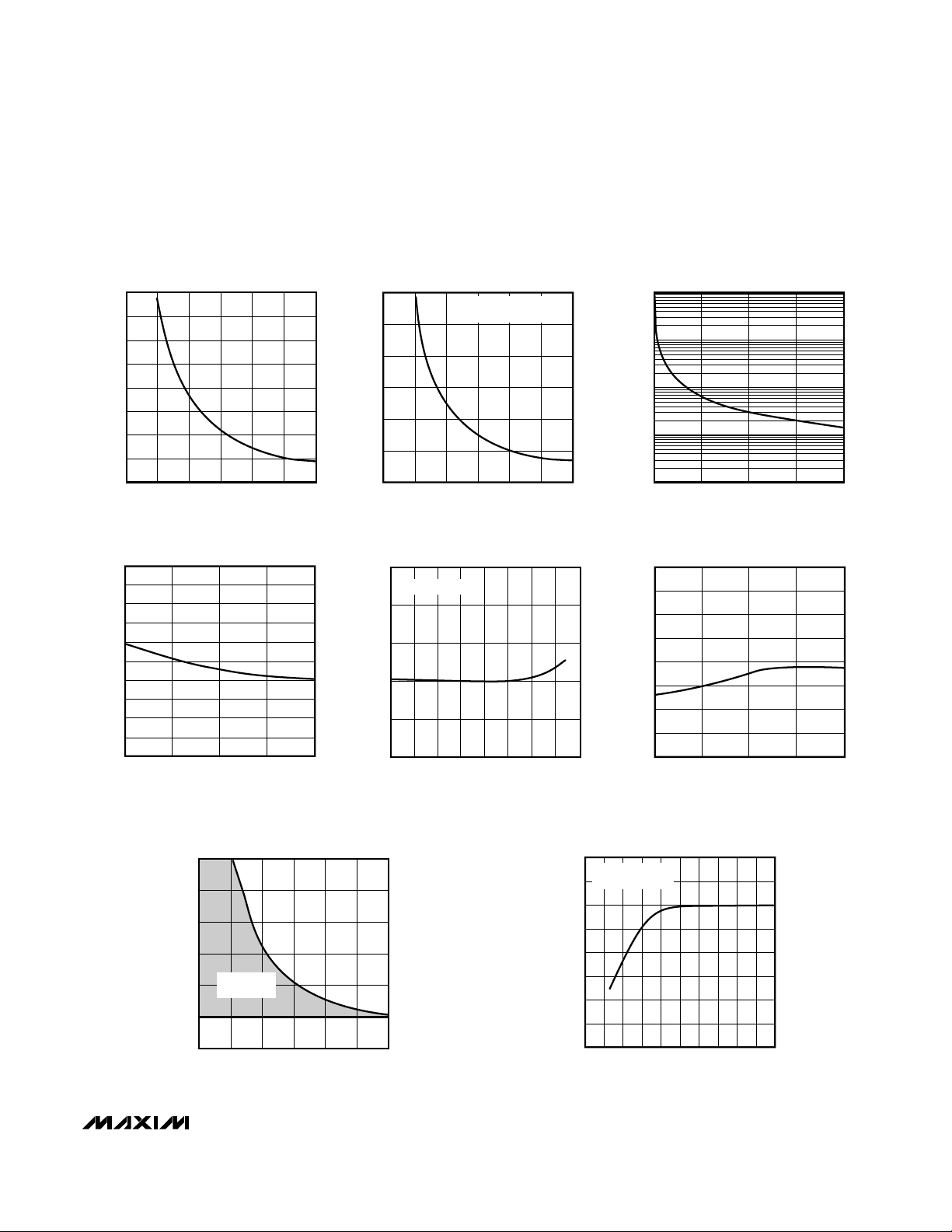
__________________________________________Typical Operating Characteristics
(MAX3263CAG loads at OUT+ and OUT- = 25Ω, V
CC
= VCCA = VCCB = +5V, TA= +25°C, unless otherwise noted.)
R
vs. BIAS CURRENT
BIASSET
02040
I
(mA)
BIAS
MAX3263-01
(kΩ)
R
60
(kΩ)
BIASSET
R
8
7
6
5
4
3
2
1
0
PERCENT CHANGE IN MODULATION
CURRENT vs. TEMPERATURE
10
8
6
4
2
0
-2
-4
% CHANGE (w.r.t. +25°C)
-6
-8
-10
02040
TEMPERATURE (°C)
MAX3263-04
8060
R
vs. MODULATION CURRENT
MODSET
12
10
8
6
MODSET
4
2
0
0 5 10 15 20 25
MODULATION CURRENT (mAp-p)
DIFFERENTIAL INPUT
SWING = 1100 mVp-p
30
MAX3263-02
1,000,000
100,000
(Ω)
10,000
PINSET
R
1000
100
PERCENT CHANGE IN BIAS
CURRENT vs. TEMPERATURE
3
APC DISABLED
2
1
0
% CHANGE (w.r.t. +25°C)
-1
-2
02040
TEMPERATURE (°C)
MAX3263-05
806010 30 7050
50
48
46
44
42
40
SUPPLY CURRENT (mA)
38
36
34
R
vs. MONITOR CURRENT
PINSET
0 500
MONITOR CURRENT (µA)
SUPPLY CURRENT
vs. TEMPERATURE
02040
TEMPERATURE (°C)
1000
8060
MAX3263-03
MAX3263-06
ALLOWABLE R
vs. MODULATION CURRENT
12
10
(kΩ)
OSADJ
ALLOWABLE R
8
6
ALLOWABLE
4
2
0
RANGE
0 5 10 15 20 25
MODULATION CURRENT (mAp-p)
OSADJ
RANGE
30
MAX3263-07
MAXIMUM MODULATION CURRENT
vs. MINIMUM DIFFERENTIAL
INPUT SIGNAL AMPLITUDE
40
R
= 1.2kΩ
MODSET
R
35
(mAp-p)
30
25
20
15
10
5
MAXIMUM MODULATION CURRENT
0
= 2kΩ
OSADJ
0 400 800 1200 1600
MINIMUM DIFFERENTIAL
INPUT SIGNAL AMPLITUDE
(mVp-p)
MAX3263-08
2000

MAX3263
Single +5V, Fully Integrated,
155Mbps Laser Diode Driver
4 _______________________________________________________________________________________
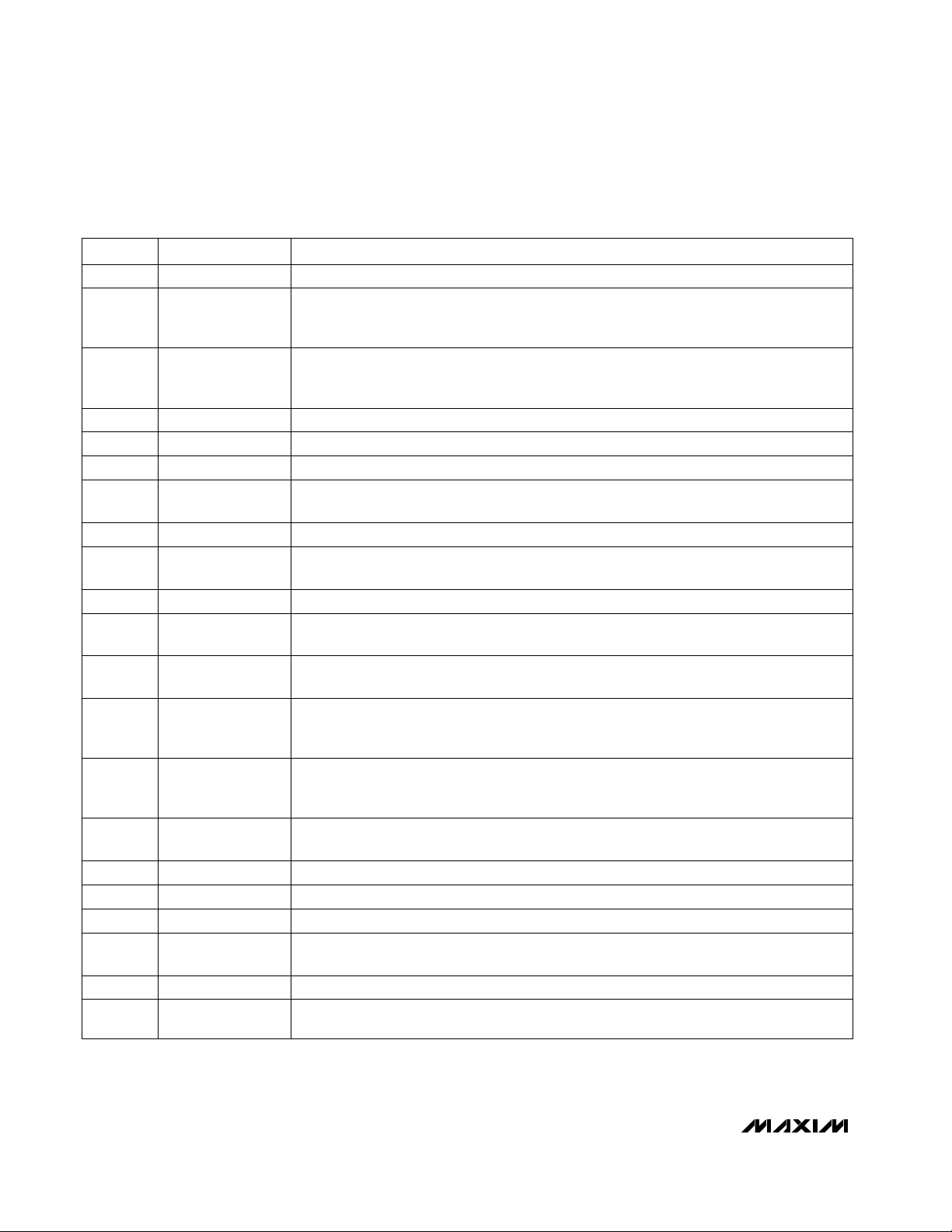
______________________________________________________________Pin Description
NAME FUNCTIONPIN
10 ENB+
Noninverting Enable TTL Input. Output currents are enabled only when ENB+ is high and
ENB- is low.
1 VREF2 Temperature-Compensated Reference Output. VREF2 is internally connected to VREF1.
12 OSADJ
Overshoot-Adjust Input. Connect to internal voltage reference through a resistor to adjust the
overshoot of the modulation output signal (see
Typical Operating Characteristics
).
11 VREF1 Temperature-Compensated Reference Output. VREF1 is internally connected to VREF2.
13 IBIASFB
Bias-Feedback Current Output. Output from automatic power-control circuit. Connect to
I
BIASSET
when using APC.
14 IBIASSET
Laser Bias Current-Programming Input. Connect to internal voltage reference through a resistor to set bias current (see
Typical Operating Characteristics
).
I
BIASOUT
= 40 x (I
BIASSET
+ I
BIASFB
).
15 IMODSET
Laser Modulation Current-Programming Input. Connect to internal voltage reference through
a resistor to set modulation current (see
Typical Operating Characteristics
).
I
MOD
= 20 x I
MODSET
.
16 IBIASOUT
Laser Bias Current Output. Connect to laser cathode through an R-L filter network (see the
Bias Network Compensation
section).
17, 19, 21 GNDA Ground for Bias and Modulation Current Drivers
22 VCCA
+5V Supply Voltage for Bias and Modulation Current Drivers. Connect VCCA to the same
potential as VCCB, but provide separate bypassing for VCCA and VCCB.
20 OUT+ Modulation Output. When VIN+ is low and VIN- is high, OUT+ sinks I
MOD
.
9 ENB- Inverting Enable TTL Input. Output currents are enabled only when ENB+ is high and ENB- is low.
8 VCCB
+5V Supply Voltage for Voltage Reference and Automatic Power-Control Circuitry. Connect
VCCB to the same potential as VCCA, but provide separate bypassing for VCCA and VCCB.
6 VIN- Inverting PECL Data Input
5 VIN+ Noninverting PECL Data Input
4, 7 GNDB Ground for Voltage Reference and Automatic Power-Control Circuitry
3 FAILOUT
Failout Output. Active-low, open-collector TTL output indicates if automatic power-control
loop is out of regulation due to insufficient monitor-diode current (when VPIN is below the
2.6V threshold). Connect FAILOUT to VCC through a 2.7kΩ pull-up resistor.
2 IPINSET
Monitor Photodiode Programming Input. Connect INPINSET to VREF1 or VREF2 through a
resistor to set the monitor current when using automatic power control (see
Typical Operating
Characteristics
).
18 OUT- Modulation Output. When VIN+ is high and VIN- is low, OUT- sinks I
MOD
.
23 IPIN Monitor Photodiode Current Input. Connect IPIN to photodiode’s anode.
24 SLWSTRT
Slow-Start Capacitor Input. Connect capacitor to ground or leave unconnected to set start-up
time, t
STARTUP
= 25.4kΩ (C
SLWSTRT
+ 2pF).
 Loading...