________________General Description
The MAX3262 limiting amplifier with its high gain and
wide bandwidth is ideal for use as a post amplifier in
fiber-optic receivers with data rates up to 1Gbps. The
amplifier’s gain can be adjusted between 33dB and
48dB. At maximum gain, signals as small as 6mVp-p
can be amplified to drive devices with PECL inputs.
The MAX3262 has complementary loss-of-signal outputs for interfacing with open-fiber-control (OFC) circuitry. These outputs can be programmed to assert
with input levels between 9mVp-p and 48mVp-p. LOS
hysteresis for any programmed level is nominally
3.0dB, preserving a balance between noise immunity
and dynamic range.
________________________Applications
1062Mbps Fibre Channel
622Mbps SONET
____________________________Features
♦ 900MHz Bandwidth
♦ 48dB Maximum Gain
♦ Chatter-Free LOS
♦ Programmable LOS Threshold
♦ Single +5V Power Supply
♦ Fully Differential Architecture
_______________Ordering Information
MAX3262
1Gbps, High-Speed Limiting Amplifier with
Chatter-Free Loss-of-Signal Detection
________________________________________________________________
Maxim Integrated Products
1
MAX3262
MAX3260
0.01µF
V
CC
ENB
DIN-
DIN+
RECEIVER WITH
PECL TERMINATIONS
(50Ω TO V
CC
- 2V)
DOUT-
DOUT+
LOSB
GND
OUTPUT
C
IN
C
IN
INPUT
FILTER
LOS
LOSB
LOS
CZN
CZP
V
CC
GND
C
AZ
+5V
+5V
50Ω +5V
+5V
+5V
C1
0.01µF
C1
R2
R1
R
4.7k
R
4.7k
V
CC
A
V
CC
B
V
CC
C
V
CC
D
V
CC
E
V
LOS
DIV2
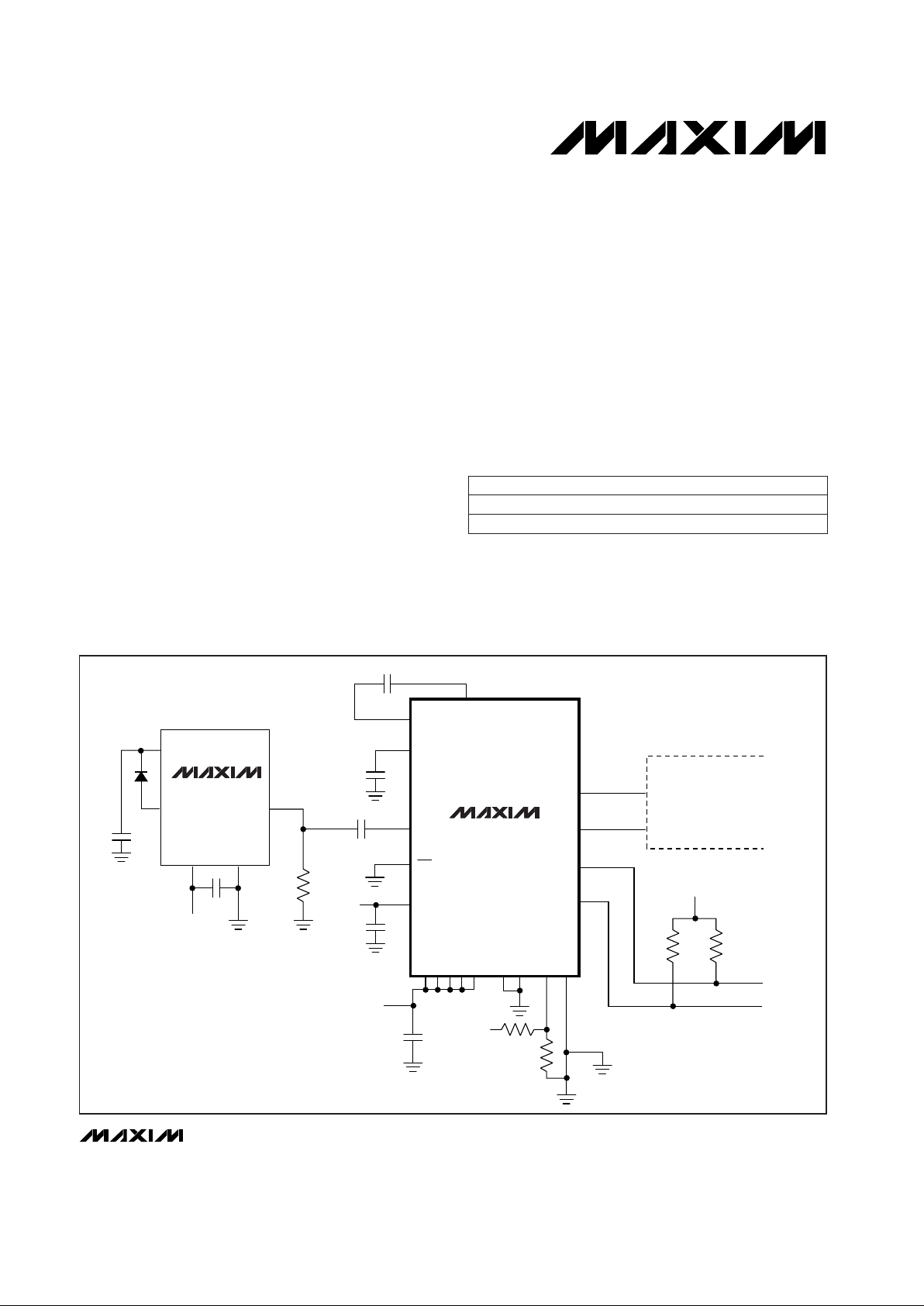
____________________________________________________Typical Operating Circuit
19-0324; Rev 2; 12/97
PART
MAX3262CAG 0°C to +70°C (T
A
)
TEMP. RANGE PIN-PACKAGE
24 SSOP
Pin Configuration appears at end of data sheet.
MAX3262C/D 0°C to +100°C (TJ) Dice*
For free samples & the latest literature: http://www.maxim-ic.com, or phone 1-800-998-8800.
For small orders, phone 408-737-7600 ext. 3468.
*Dice are designed to operate over this range but are tested and
guaranteed only at TA= +25°C.

MAX3262
1Gbps, High-Speed Limiting Amplifier with
Chatter-Free Loss-of-Signal Detection
2 _______________________________________________________________________________________
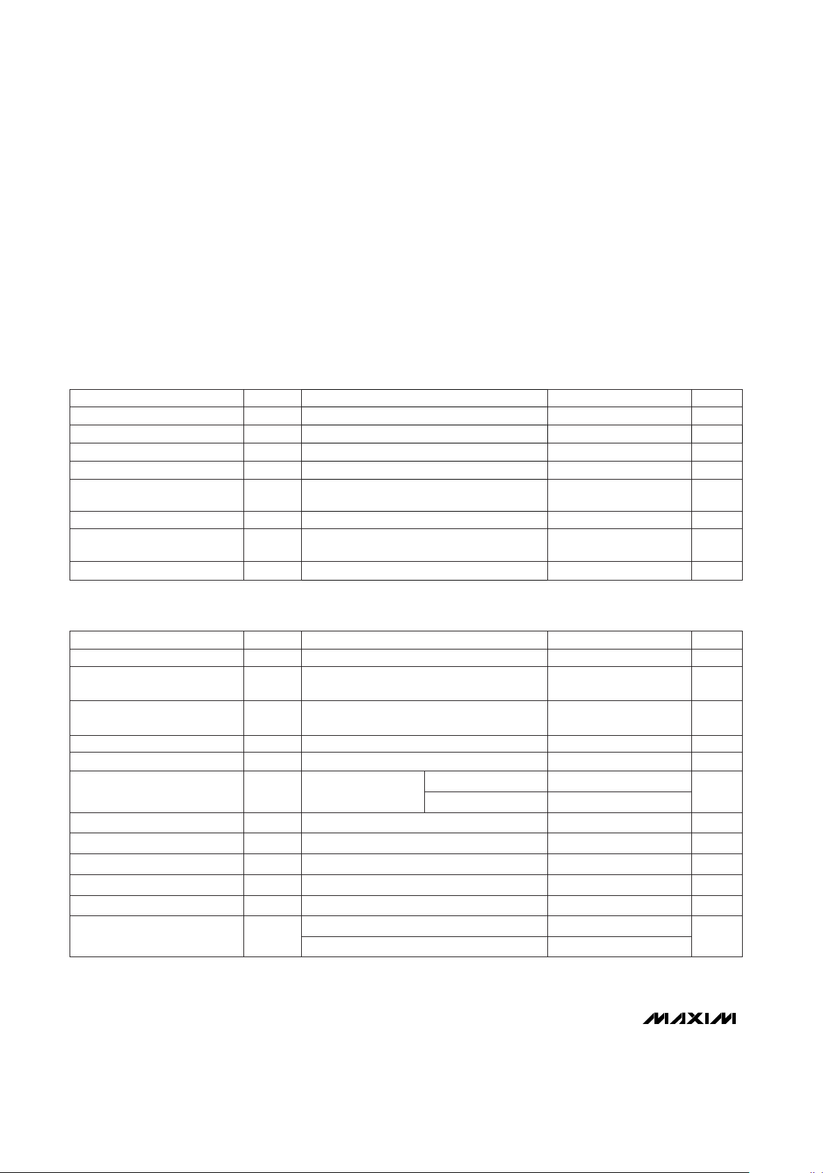
ABSOLUTE MAXIMUM RATINGS
DC ELECTRICAL CHARACTERISTICS
(VCC= +5V, R
LOAD
= 50Ω to VCC- 2V (equivalent), TA= 0°C to +70°C. Typical values are at VCC= 5V and TA= +25°C.)
AC ELECTRICAL CHARACTERISTICS
(VCC= +5V, R
LOAD
= 50Ω to 3V, AC parameters are not tested, TA= +25°C, unless otherwise noted.)
Stresses beyond those listed under “Absolute Maximum Ratings” may cause permanent damage to the device. These are stress ratings only, and functional
operation of the device at these or any other conditions beyond those indicated in the operational sections of the specifications is not implied. Exposure to
absolute maximum rating conditions for extended periods may affect device reliability.
Note 1: Input is a 200MHz square wave, tR< 300ps, 8mVp-p.
Note 2: Input is a 200MHz square wave, t
R
< 300ps, 1.8Vp-p.
Note 3: Input-referred noise = RMS output noise/low-frequency gain.
Power Supply, V
CC
- VEE......................................................6.0V
Input Voltage, DIN+, DIN-.....................................................6.0V
CZN, CZP, ENB, VLOS, DIV2, LOS+, LOS-.....-0.3V, V
CC
+ 0.3V
DOUT+, DOUT- (with 50Ω load).......................2.5V, V
CC
+ 0.3V
Continuous Power Dissipation (T
A
= +70°C)
SSOP (derate 10mW/°C above +70°C) ....................500mW°C
Junction Operating Temperature ......................-55°C to +150°C
Storage Temperature Range.............................-55°C to +175°C
Processing Temperature (Die).........................................+400°C
No output load
VCC= 5.0V
I
OUT
= -1.0mA
DIV2 = 0V
CONDITIONS
µA150I
ENB
Enable Input Current
mA60I
VCC
Power-Supply Current
V2.5 3.0V
DIN
Input Bias Voltage
µA120I
LOS
V
LOS
Input Current
V3.5 3.7 3.8Common-Mode Output Voltage
V0.5
LOS+, LOS- Output Low
Voltage
mA0.5DIV2 Short-Circuit Current
UNITSMIN TYP MAXSYMBOLPARAMETER
mV±35
Differential Output Offset,
DOUT+ to DOUT-
MAX3262CAG
MHz
MAX3262C/D
V
OH
- V
OL
1Gbps, 8mVp-p input
V
LOS
= 5V, DIV2 = GND (Note 3)
V
LOS
= 5V, Pattern 27 - 1PRBS
750 810
Peak-to-peak
(Note 1)
(Note 2) µs
Input referred, 55MHz
CONDITIONS
BWSmall-Signal Bandwidth
Differential inputs,
peak-to-peak
mV
10 48
V
SR
LOS Sensitivity Range
800 925
mV400 600 730V
OUT
Output Voltage Amplitude
ps250t
R, tF
Output Edge Speed
ps40PWDPulse-Width Distortion
µV80V
n
Differential Input Noise
dB1.5 3.0 5.0HYSLOS Hysteresis
V
9 48MAX3262C/D
MAX3262CAG
µs0.020 0.5t
OFFL
LOS Release Time,
Minimum Input
0.5t
OFFH
LOS Release Time,
Maximum Input
(Note 1)
dB35PSRRPower-Supply Rejection Ratio
µs0.2 0.5t
ONL
LOS Assert Time
UNITSMIN TYP MAXSYMBOLPARAMETER
0.006 1.8V
ID
Input Voltage Range

MAX3262
1Gbps, High-Speed Limiting Amplifier with
Chatter-Free Loss-of-Signal Detection
_______________________________________________________________________________________
3
70
65
60
55
50
45
40
VCC SUPPLY CURRENT
(NO OUTPUT LOAD) vs. TEMPERATURE
MAX3262-01
SUPPLY CURRENT (mA)
0 10 20 30 40 50 60 70 80 90 100
TEMPERATURE (°C)
5.25V
5.0V
4.75V
0
0
LOS HYSTERESIS
vs. TEMPERATURE
MAX3262-02
TEMPERATURE (°C)
HYSTERESIS (dB)
20 40 60 80 100 120
1
2
3
4
5
6
7
8
1Gbps WITH 1,0 PATTERN
4.0
400
LOS SENSITIVITY
vs. FREQUENCY
MAX3262-03
FREQUENCY (Mbps)
SENSITIVITY (mVp-p)
600 800 1000
4.5
5.0
5.5
6.0
6.5
7.0
7.5
8.0
1-0 PATTERN
K28.5 SEQUENCE
(FIBRE CHANNEL IDLE PATTERN)
PRBS 27-1
4.0
3.0
2.0
1.0
0
3.2 3.4 3.6 3.8 4.0 4.2 4.4 4.6 4.8 5.0
LOS HYSTERESIS vs. V
LOS
MAX3262-04
V
LOS
(V)
5.0
HYSTERESIS (dB)
1Gbps
DIV2 = 0
1,0 PATTERN
25
0
FREQUENCY RESPONSE
MAX3262-05
FREQUENCY (MHz)
GAIN (dB)
200 400 600 800 1000 1200 1400
31
37
43
49
55
V
LOS
= 5V
DIV2 = GND
V
LOS
= 5V
DIV2 OPEN
V
LOS
= 3.4V
DIV2 OPEN
V
LOS
= 3.0V
DIV2 OPEN
EYE DIAGRAM
1Gbps
R
LOAD
= 50Ω to VCC - 2V (EQUIVALENT)
V
IN
= 250mV, V
CC
= +5V, DIV2 = GND, V
LOS
= V
CC
V
LOS
= V
CC
MAX3262-07
+500mV
100mV/div
-500mV
225ps/div
LOS
OUTPUT
DATA
INPUT
LOS OPERATION
MAX3262-06
2µs/div
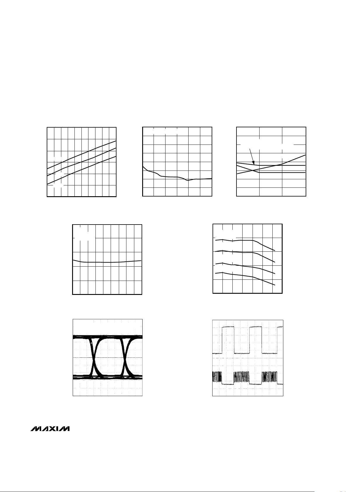
__________________________________________Typical Operating Characteristics
(VCC= 5V, TA = +25°C, unless otherwise noted.)
 Loading...