Maxim MAX3261ECJ, MAX3261E-D, MAX3261CCJ Datasheet

_______________General Description
The MAX3261 is a complete, easy-to-program, single
+5V-powered, 1.25Gbps laser diode driver with complementary enable inputs and automatic power control
(APC). The MAX3261 accepts differential PECL inputs
and provides complementary output currents. A temperature-stabilized reference voltage is provided to
simplify laser current programming. This allows modulation current to be programmed up to 30mA and bias
current to be programmed up to 60mA with two external resistors.
Complementary enable inputs allow the MAX3261 to
interface with open-fiber-control architecture—a feature
not found in other 1.25Gbps laser diode drivers.
An APC circuit is provided to maintain constant laser power
in transmitters that use a monitor photodiode. Only two
external components are required to implement the APC
function.
The MAX3261’s fully integrated feature set includes a
TTL-compatible laser failure indicator and a programmable slow-start circuit to prevent laser damage. The
slow-start is preset to 50ns and can be extended by
adding an external capacitor.
________________________Applications
Laser Diode Transmitters
531Mbps and 1062Mbps Fibre Channel
622Mbps SDH/SONET
Gigabit Ethernet
____________________________Features
♦ Rise Times Less than 250ps
♦ Differential PECL Inputs
♦ Single +5V Supply
♦ Automatic Power Control
♦ Temperature-Compensated Reference Voltage
♦ Complementary Enable Inputs
______________Ordering Information
MAX3261
Single +5V, Fully Integrated,
1.25Gbps Laser Diode Driver
________________________________________________________________
Maxim Integrated Products
1
TQFP
TOP VIEW
IMODSET
IBIASSET
IBIASFB
OSADJ
VREF1
IBIASOUT
ENB+
V
CC
B
GNDA
IPIN
SLWSTRT
GNDB
VREF2
GNDA
FAILOUT
IPINSET
V
CC
A
V
CC
A
OUT-
GNDA
OUT+
GNDA
V
CC
A
GNDA
VIN+
GNDB
V
CC
B
VIN-
GNDB
V
CC
B
GNDB
ENB-
16
15
14
13
12
11
10
9
17
18
19
20
21
22
23
24
25
26
27
28
29
30
31
32
8
7
6
5
4
3
2
1
MAX3261
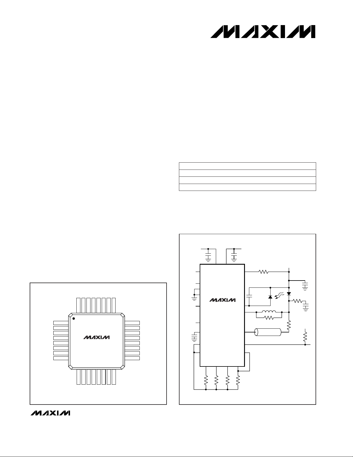
__________________Pin Configuration
19-0323; Rev 4; 8/97
PART
MAX3261CCJ 0°C to +70°C
TEMP. RANGE PIN-PACKAGE
32 TQFP
MAX3261
+5V +5V
+5V
+5V
OUT+
OUT-
2.7k
IPIN
PECL
INPUTS
TO OPEN
FIBER
CONTROL
IBIASOUT
FAILOUT
IBIASFB
OSADJ
IMODSET
IPINSET
IBIASSET
VCCAVCCB
ZO = 25Ω
MICROSTRIP
VIN+
VIN-
ENB+
GND B
GND A
ENB-
SLWSTRT
VREF1
VREF2
LASER
PHOTO-
DIODE
__________Typical Operating Circuit
MAX3261ECJ -40°C to +85°C 32 TQFP
MAX3261E/D -40°C to +85°C Dice*
*
Dice are designed to operate over a -40°C to +140°C junction
temperature (Tj) range. Tested and guaranteed at Tj = +25°C.
For free samples & the latest literature: http://www.maxim-ic.com, or phone 1-800-998-8800.
For small orders, phone 408-737-7600 ext. 3468.

MAX3261
Single +5V, Fully Integrated,
1.25Gbps Laser Diode Driver
2 _______________________________________________________________________________________
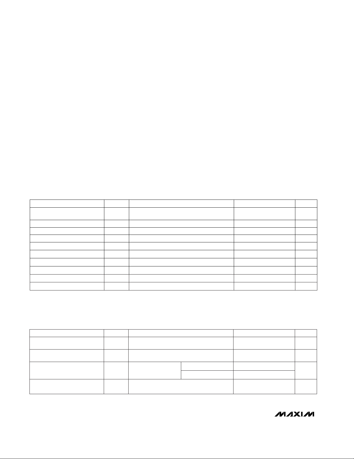
ABSOLUTE MAXIMUM RATINGS
DC ELECTRICAL CHARACTERISTICS
(VCC= VCCA = VCCB = +4.75V to +5.25V, TA= T
MIN
to T
MAX
, unless otherwise noted. Typical values are at VCC= +5V and
TA= +25°C.) (Note 1)
Stresses beyond those listed under “Absolute Maximum Ratings” may cause permanent damage to the device. These are stress ratings only, and functional
operation of the device at these or any other conditions beyond those indicated in the operational sections of the specifications is not implied. Exposure to
absolute maximum rating conditions for extended periods may affect device reliability.
Terminal Voltage (with respect to GND)
Supply Voltages (V
CC
A, VCCB)...............................-0.3V to 6V
VIN+, VIN-, FAILOUT...............................................0V to V
CC_
OUT+, OUT-, IBIASOUT.......................................1.5V to V
CC_
ENB+, ENB-.......................V
CC_
or 5.5V, whichever is smaller
Differential Input Voltage (
|
VIN+ - VIN-|)...........................3.8V
Input Current
IBIASOUT............................................................0mA to 75mA
OUT+, OUT-........................................................0mA to 40mA
IBIASSET........................................................0mA to 1.875mA
IMODSET...............................................................0mA to 2mA
IPIN, IPINSET, OSADJ...........................................0mA to 2mA
FAILOUT..............................................................0mA to 10mA
IBIASFB................................................................-2mA to 2mA
Output Current
VREF1, VREF2.....................................................0mA to 20mA
SLWSTRT ..............................................................0mA to 5mA
Continuous Power Dissipation (T
A
= +70°C)
TQFP (derate 10.2mW/°C above +70°C)......................816mW
Operating Temperature Ranges
MAX3261CCJ......................................................0°C to +70°C
MAX3261ECJ ...................................................-40°C to +85°C
Junction Temperature......................................................+150°C
Storage Temperature Range.............................-55°C to +175°C
Processing Temperature (die).........................................+400°C
TA= +25°C
(Note 2)
CONDITIONS
mA12I
REF
Available Reference Current
V3.15 3.3 3.45V
REF
mA60I
BIAS
Range of Programmable Laser
Bias Current
Reference Voltage
V0.8V
IL
TTL Input Low
mA50I
VCC
Supply Current
VVCC- 1.165V
IH
PECL Input High
VVCC- 1.475V
IL
PECL Input Low
V2V
IH
TTL Input High
UNITSMIN TYP MAXSYMBOLPARAMETER
AC ELECTRICAL CHARACTERISTICS
(VCC= VCCA = VCCB = +4.75V to +5.25V, R
LOAD
(at OUT+ and OUT-) = 25Ωconnected to VCC, TA= -40°C to +85°C, unless other-
wise noted. Typical values are at VCC= +5V and TA= +25°C.) (Note 3)
Minimum differential input
swing is 1100mVp-p (Note 4)
CONDITIONS
mA30I
MOD
Range of Programmable
Modulation Current
UNITSMIN TYP MAXSYMBOLPARAMETER
I
BIAS
= 25mA, I
MOD
= 12mA, 4ns unit
interval; measured from 10% to 90%.
ps250tR, t
F
Modulation-Current Rise and
Fall Time
I
MOD
= 12mA,
TA= +25°C
%
±10
Aberrations, Rising and Falling
Edge
I
BIAS
= 25mA, I
MOD
= 12mA, 4ns unit interval ps80PWD
Modulation-Current PulseWidth Distortion
±15
Loaded with 2.7kΩpull-up resistor to V
CC
V4.5V
OH
FAILOUT Output High
Loaded with 2.7kΩpull-up resistor to V
CC
V0.5V
OL
FAILOUT Output Low
Note 1: Dice are tested at TA= +25°C.
Note 2: I
VCC
= I
VCC
A + I
VCC
B, I
BIAS
= 60mA, I
MOD
= 30mA, and I
PIN
= 140µA.
Note 3: AC characteristics are guaranteed by design and characterization.
Note 4: An 1100mVp-p differential is equivalent to complementary 550mVp-p signals on VIN+ and VIN-.
MAX3261E/D
MAX3261ECJ

MAX3261
Single +5V, Fully Integrated,
1.25Gbps Laser Diode Driver
_______________________________________________________________________________________
3
-250mV
250.3mV
38.23ns 200ps/div
EYE DIAGRAM
(622Mbps, LOAD = 25Ω, NOT FILTERED)
MAX3261-1
50mV/div
40.23ns
-35mV
265mV
38.14ns 200ps/div
EYE DIAGRAM
(622Mbps, LOAD AT OUT- = 1300nm
LASER WITH 467MHz BESSEL FILTER)*
MAX3261-2
30mV/div
40.14ns
-250mV
250.3mV
38.13ns 117ps/div
EYE DIAGRAM
(1062Mbps, LOAD = 25Ω, NOT FILTERED)
MAX3261-3
50mV/div
39.3ns
-50mV
450mV
38.74ns 117ps/div
EYE DIAGRAM
(1062Mbps, LOAD AT OUT- = 1300nm
LASER WITH 800MHz BESSEL FILTER)*
MAX3261-4
50mV/div
39.91ns
-35mV
265mV
38.15ns 200ps/div
MAX3261CCJ EYE DIAGRAM
(622Mbps, LOAD AT OUT- = 1300nm
LASER WITH 467MHz BESSEL FILTER)*
MAX3261-5
30mV/div
40.15ns
-66.2mV
513.7mV
37.78ns 117ps/div
MAX3261CCJ EYE DIAGRAM
(1062Mbps, LOAD AT OUT- = 1300nm
LASER WITH 800MHz BESSEL FILTER)*
MAX3261-6
58mV/div
38.95ns
100
0 500
R
PINSET
vs. MONITOR CURRENT
MAX3261-09
MONITOR CURRENT (µA)
R
PINSET
(Ω)
1000
10,000
1000
100,000
1,000,000
0
0 20 40
R
BIASSET
vs. BIAS CURRENT
5
MAX3261-07
I
BIAS
(mA)
R
BIASSET
(kΩ)
60
3
1
4
2
6
7
8
* LASER = EPITAXX EDL 1300RFC TO-STYLE HEADER
0
0 5 10 15 20 25
R
MODSET
vs. MODULATION CURRENT
8
MAX3261-08
MODULATION CURRENT (mAp-p)
R
MODSET
(kΩ)
30
6
4
2
10
12
DIFFERENTIAL INPUT
SWING = 1100 mVp-p
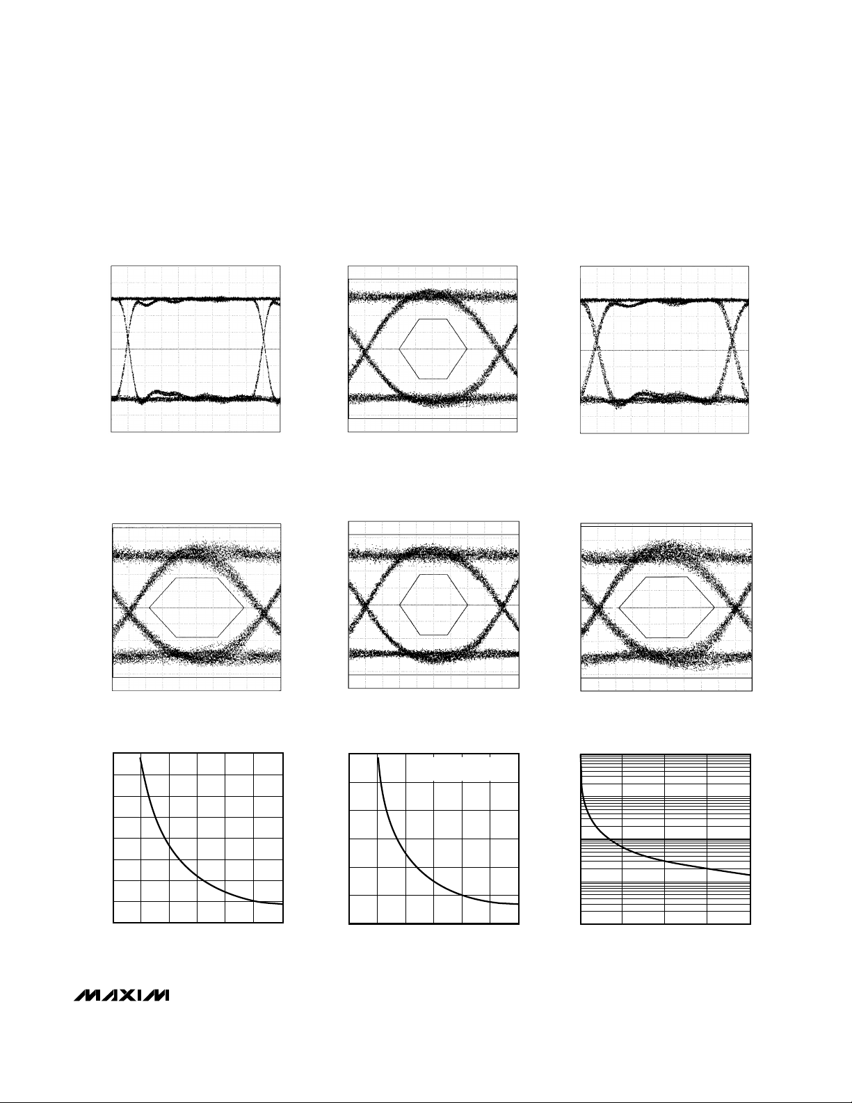
__________________________________________Typical Operating Characteristics
(MAX3261E/D, load at OUT+ and OUT- = 25Ω, VCC= VCCA = VCCB = +5V, TA= +25°C, unless otherwise noted.)

MAX3261
Single +5V, Fully Integrated,
1.25Gbps Laser Diode Driver
4 _______________________________________________________________________________________
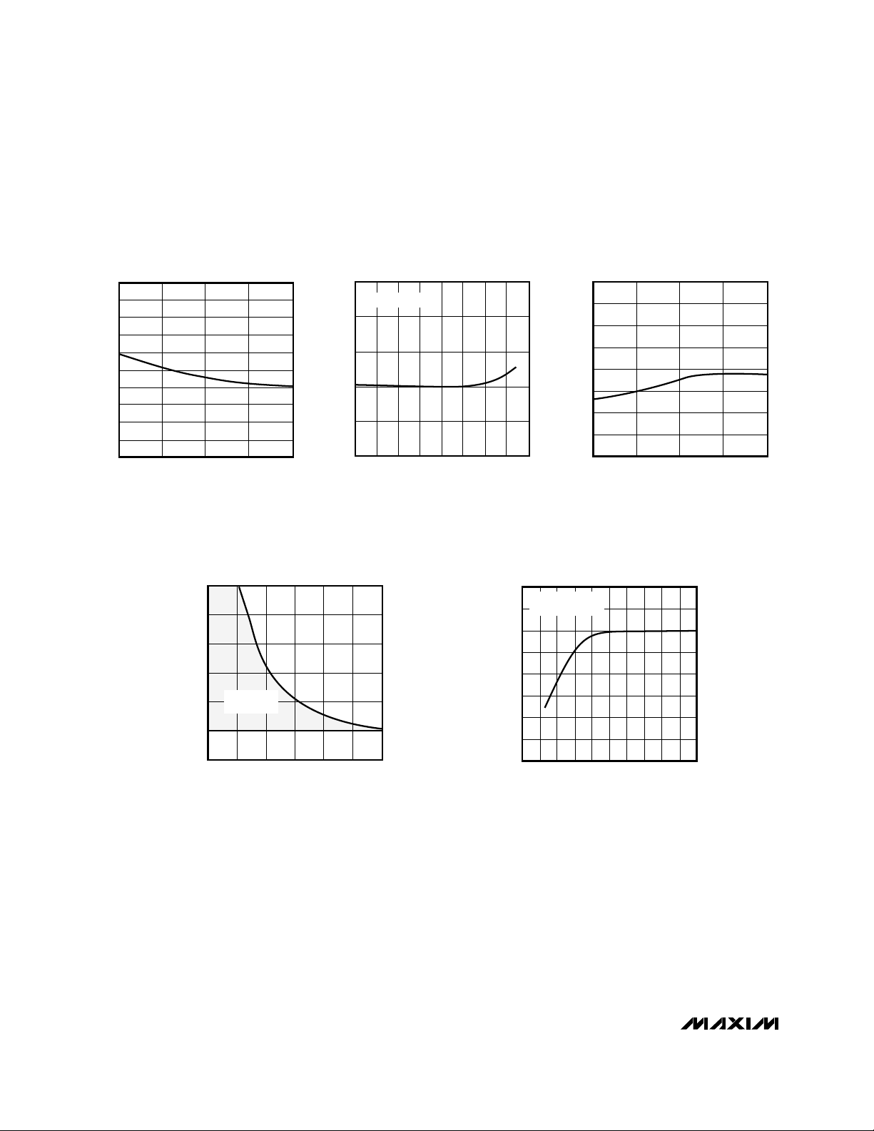
____________________________Typical Operating Characteristics (continued)
(MAX3261E/D, LOAD at OUT+ = OUT- = 25Ω, VCC= VCCA = VCCB = +5V, TA = +25°C, unless otherwise noted.)
-2
-1
0
1
2
3
0 20 40
PERCENT CHANGE IN BIAS
CURRENT vs. TEMPERATURE
MAX3261-11
TEMPERATURE (°C)
% CHANGE (w.r.t. +25°C)
806010 30 7050
APC DISABLED
34
36
38
40
42
44
46
48
50
0 20 40
SUPPLY CURRENT
vs. TEMPERATURE
MAX3261-12
TEMPERATURE (°C)
SUPPLY CURRENT (mA)
8060
-10
-8
-6
-4
-2
0
2
4
6
8
10
0 20 40
PERCENT CHANGE IN MODULATION
CURRENT vs. TEMPERATURE
MAX3261-10
TEMPERATURE (°C)
% CHANGE (w.r.t. +25°C)
8060
0
0 5 10 15 20 25
ALLOWABLE R
OSADJ
vs. MODULATION CURRENT
8
MAX3261-13
MODULATION CURRENT (mAp-p)
ALLOWABLE R
OSADJ
(kΩ)
30
6
4
2
10
12
ALLOWABLE
RANGE
0
0 400 800 1200 1600
MAXIMUM MODULATION CURRENT
vs. MINIMUM DIFFERENTIAL
INPUT SIGNAL AMPLITUDE
25
MAX3261-14
MINIMUM DIFFERENTIAL
INPUT SIGNAL AMPLITUDE
(mVp-p)
MAXIMUM MODULATION CURRENT
(mAp-p)
2000
20
15
10
5
30
35
40
R
MODSET
= 1.2kΩ
R
OSADJ
= 2kΩ
 Loading...