

Page 1
现货库存、技术资料、百科信息、热点资讯,精彩尽在鼎好!
_______________General Description
The MAX3261 is a complete, easy-to-program, single
+5V-powered, 1.25Gbps laser diode driver with complementary enable inputs and automatic power control
(APC). The MAX3261 accepts differential PECL inputs
and provides complementary output currents. A temperature-stabilized reference voltage is provided to
simplify laser current programming. This allows modulation current to be programmed up to 30mA and bias
current to be programmed up to 60mA with two external resistors.
Complementary enable inputs allow the MAX3261 to
interface with open-fiber-control architecture—a feature
not found in other 1.25Gbps laser diode drivers.
An APC circuit is provided to maintain constant laser power
in transmitters that use a monitor photodiode. Only two
external components are required to implement the APC
function.
The MAX3261’s fully integrated feature set includes a
TTL-compatible laser failure indicator and a programmable slow-start circuit to prevent laser damage. The
slow-start is preset to 50ns and can be extended by
adding an external capacitor.
________________________Applications
Laser Diode Transmitters
531Mbps and 1062Mbps Fibre Channel
622Mbps SDH/SONET
Gigabit Ethernet
____________________________Features
♦ Rise Times Less than 250ps
♦ Differential PECL Inputs
♦ Single +5V Supply
♦ Automatic Power Control
♦ Temperature-Compensated Reference Voltage
♦ Complementary Enable Inputs
______________Ordering Information
MAX3261
Single +5V, Fully Integrated,
1.25Gbps Laser Diode Driver
________________________________________________________________
Maxim Integrated Products
1
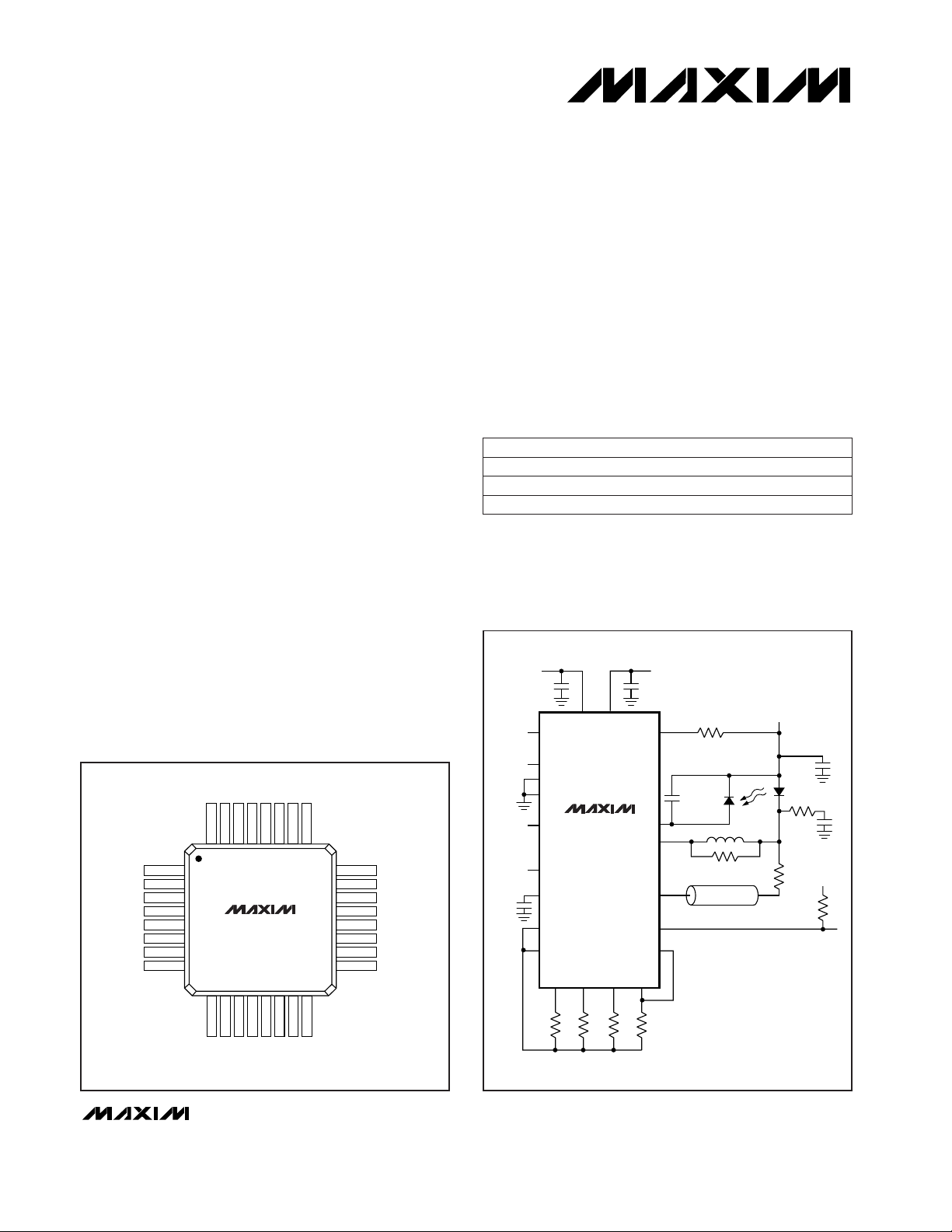
TQFP
TOP VIEW
IMODSET
IBIASSET
IBIASFB
OSADJ
VREF1
IBIASOUT
ENB+
V
CC
B
GNDA
IPIN
SLWSTRT
GNDB
VREF2
GNDA
FAILOUT
IPINSET
V
CC
A
V
CC
A
OUT-
GNDA
OUT+
GNDA
V
CC
A
GNDA
VIN+
GNDB
V
CC
B
VIN-
GNDB
V
CC
B
GNDB
ENB-
16
15
14
13
12
11
10
9
17
18
19
20
21
22
23
24
25
26
27
28
29
30
31
32
8
7
6
5
4
3
2
1
MAX3261
__________________Pin Configuration
19-0323; Rev 4; 8/97
PART
MAX3261CCJ 0°C to +70°C
TEMP. RANGE PIN-PACKAGE
32 TQFP
MAX3261
+5V +5V
+5V
+5V
OUT+
OUT-
2.7k
IPIN
PECL
INPUTS
TO OPEN
FIBER
CONTROL
IBIASOUT
FAILOUT
IBIASFB
OSADJ
IMODSET
IPINSET
IBIASSET
VCCAVCCB
ZO = 25Ω
MICROSTRIP
VIN+
VIN-
ENB+
GND B
GND A
ENB-
SLWSTRT
VREF1
VREF2
LASER
PHOTO-
DIODE
__________Typical Operating Circuit
MAX3261ECJ -40°C to +85°C 32 TQFP
MAX3261E/D -40°C to +85°C Dice*
*
Dice are designed to operate over a -40°C to +140°C junction
temperature (Tj) range. Tested and guaranteed at Tj = +25°C.
For free samples & the latest literature: http://www.maxim-ic.com, or phone 1-800-998-8800.
For small orders, phone 408-737-7600 ext. 3468.
Page 2
MAX3261
Single +5V, Fully Integrated,
1.25Gbps Laser Diode Driver
2 _______________________________________________________________________________________
ABSOLUTE MAXIMUM RATINGS
DC ELECTRICAL CHARACTERISTICS
(VCC= VCCA = VCCB = +4.75V to +5.25V, TA= T
MIN
to T
MAX
, unless otherwise noted. Typical values are at VCC= +5V and
TA= +25°C.) (Note 1)
Stresses beyond those listed under “Absolute Maximum Ratings” may cause permanent damage to the device. These are stress ratings only, and functional
operation of the device at these or any other conditions beyond those indicated in the operational sections of the specifications is not implied. Exposure to
absolute maximum rating conditions for extended periods may affect device reliability.
Terminal Voltage (with respect to GND)
Supply Voltages (V
CC
A, VCCB)...............................-0.3V to 6V
VIN+, VIN-, FAILOUT...............................................0V to V
CC_
OUT+, OUT-, IBIASOUT.......................................1.5V to V
CC_
ENB+, ENB-.......................V
CC_
or 5.5V, whichever is smaller
Differential Input Voltage (
|
VIN+ - VIN-|)...........................3.8V
Input Current
IBIASOUT............................................................0mA to 75mA
OUT+, OUT-........................................................0mA to 40mA
IBIASSET........................................................0mA to 1.875mA
IMODSET...............................................................0mA to 2mA
IPIN, IPINSET, OSADJ...........................................0mA to 2mA
FAILOUT..............................................................0mA to 10mA
IBIASFB................................................................-2mA to 2mA
Output Current
VREF1, VREF2.....................................................0mA to 20mA
SLWSTRT ..............................................................0mA to 5mA
Continuous Power Dissipation (T
A
= +70°C)
TQFP (derate 10.2mW/°C above +70°C)......................816mW
Operating Temperature Ranges
MAX3261CCJ......................................................0°C to +70°C
MAX3261ECJ ...................................................-40°C to +85°C
Junction Temperature......................................................+150°C
Storage Temperature Range.............................-55°C to +175°C
Processing Temperature (die).........................................+400°C
TA= +25°C
(Note 2)
CONDITIONS
mA12I
REF
Available Reference Current
V3.15 3.3 3.45V
REF
mA60I
BIAS
Range of Programmable Laser
Bias Current
Reference Voltage
V0.8V
IL
TTL Input Low
mA50I
VCC
Supply Current
VVCC- 1.165V
IH
PECL Input High
VVCC- 1.475V
IL
PECL Input Low
V2V
IH
TTL Input High
UNITSMIN TYP MAXSYMBOLPARAMETER
AC ELECTRICAL CHARACTERISTICS
(VCC= VCCA = VCCB = +4.75V to +5.25V, R
LOAD
(at OUT+ and OUT-) = 25Ωconnected to VCC, TA= -40°C to +85°C, unless other-
wise noted. Typical values are at VCC= +5V and TA= +25°C.) (Note 3)
Minimum differential input
swing is 1100mVp-p (Note 4)
CONDITIONS
mA30I
MOD
Range of Programmable
Modulation Current
UNITSMIN TYP MAXSYMBOLPARAMETER
I
BIAS
= 25mA, I
MOD
= 12mA, 4ns unit
interval; measured from 10% to 90%.
ps250tR, t
F
Modulation-Current Rise and
Fall Time
I
MOD
= 12mA,
TA= +25°C
%
±10
Aberrations, Rising and Falling
Edge
I
BIAS
= 25mA, I
MOD
= 12mA, 4ns unit interval ps80PWD
Modulation-Current PulseWidth Distortion
±15
Loaded with 2.7kΩpull-up resistor to V
CC
V4.5V
OH
FAILOUT Output High
Loaded with 2.7kΩpull-up resistor to V
CC
V0.5V
OL
FAILOUT Output Low
Note 1: Dice are tested at TA= +25°C.
Note 2: I
VCC
= I
VCC
A + I
VCC
B, I
BIAS
= 60mA, I
MOD
= 30mA, and I
PIN
= 140µA.
Note 3: AC characteristics are guaranteed by design and characterization.
Note 4: An 1100mVp-p differential is equivalent to complementary 550mVp-p signals on VIN+ and VIN-.
MAX3261E/D
MAX3261ECJ
Page 3
MAX3261
Single +5V, Fully Integrated,
1.25Gbps Laser Diode Driver
_______________________________________________________________________________________
3
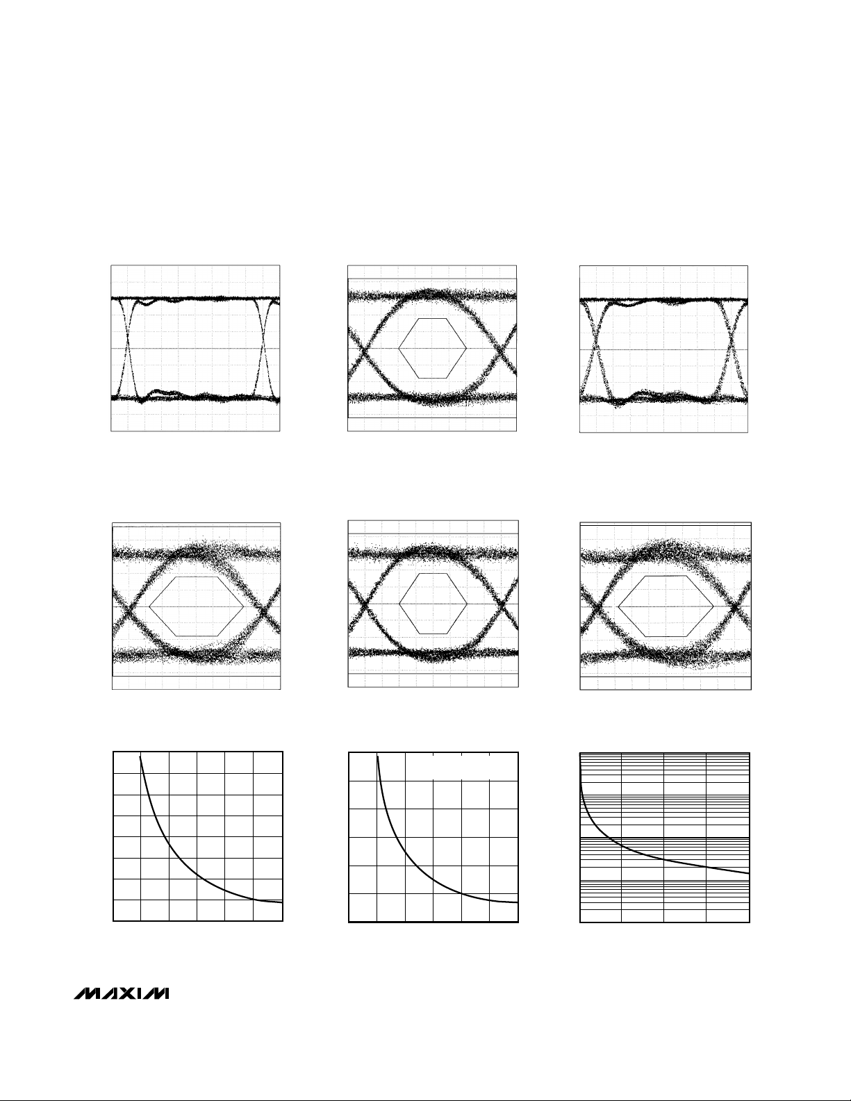
-250mV
250.3mV
38.23ns 200ps/div
EYE DIAGRAM
(622Mbps, LOAD = 25Ω, NOT FILTERED)
MAX3261-1
50mV/div
40.23ns
-35mV
265mV
38.14ns 200ps/div
EYE DIAGRAM
(622Mbps, LOAD AT OUT- = 1300nm
LASER WITH 467MHz BESSEL FILTER)*
MAX3261-2
30mV/div
40.14ns
-250mV
250.3mV
38.13ns 117ps/div
EYE DIAGRAM
(1062Mbps, LOAD = 25Ω, NOT FILTERED)
MAX3261-3
50mV/div
39.3ns
-50mV
450mV
38.74ns 117ps/div
EYE DIAGRAM
(1062Mbps, LOAD AT OUT- = 1300nm
LASER WITH 800MHz BESSEL FILTER)*
MAX3261-4
50mV/div
39.91ns
-35mV
265mV
38.15ns 200ps/div
MAX3261CCJ EYE DIAGRAM
(622Mbps, LOAD AT OUT- = 1300nm
LASER WITH 467MHz BESSEL FILTER)*
MAX3261-5
30mV/div
40.15ns
-66.2mV
513.7mV
37.78ns 117ps/div
MAX3261CCJ EYE DIAGRAM
(1062Mbps, LOAD AT OUT- = 1300nm
LASER WITH 800MHz BESSEL FILTER)*
MAX3261-6
58mV/div
38.95ns
100
0 500
R
PINSET
vs. MONITOR CURRENT
MAX3261-09
MONITOR CURRENT (µA)
R
PINSET
(Ω)
1000
10,000
1000
100,000
1,000,000
0
0 20 40
R
BIASSET
vs. BIAS CURRENT
5
MAX3261-07
I
BIAS
(mA)
R
BIASSET
(kΩ)
60
3
1
4
2
6
7
8
* LASER = EPITAXX EDL 1300RFC TO-STYLE HEADER
0
0 5 10 15 20 25
R
MODSET
vs. MODULATION CURRENT
8
MAX3261-08
MODULATION CURRENT (mAp-p)
R
MODSET
(kΩ)
30
6
4
2
10
12
DIFFERENTIAL INPUT
SWING = 1100 mVp-p
__________________________________________Typical Operating Characteristics
(MAX3261E/D, load at OUT+ and OUT- = 25Ω, VCC= VCCA = VCCB = +5V, TA= +25°C, unless otherwise noted.)
Page 4
MAX3261
Single +5V, Fully Integrated,
1.25Gbps Laser Diode Driver
4 _______________________________________________________________________________________
____________________________Typical Operating Characteristics (continued)
(MAX3261E/D, LOAD at OUT+ = OUT- = 25Ω, VCC= VCCA = VCCB = +5V, TA = +25°C, unless otherwise noted.)
-2
-1
0
1
2
3
0 20 40
PERCENT CHANGE IN BIAS
CURRENT vs. TEMPERATURE
MAX3261-11
TEMPERATURE (°C)
% CHANGE (w.r.t. +25°C)
806010 30 7050
APC DISABLED
34
36
38
40
42
44
46
48
50
0 20 40
SUPPLY CURRENT
vs. TEMPERATURE
MAX3261-12
TEMPERATURE (°C)
SUPPLY CURRENT (mA)
8060
-10
-8
-6
-4
-2
0
2
4
6
8
10
0 20 40
PERCENT CHANGE IN MODULATION
CURRENT vs. TEMPERATURE
MAX3261-10
TEMPERATURE (°C)
% CHANGE (w.r.t. +25°C)
8060
0
0 5 10 15 20 25
ALLOWABLE R
OSADJ
vs. MODULATION CURRENT
8
MAX3261-13
MODULATION CURRENT (mAp-p)
ALLOWABLE R
OSADJ
(kΩ)
30
6
4
2
10
12
ALLOWABLE
RANGE
0
0 400 800 1200 1600
MAXIMUM MODULATION CURRENT
vs. MINIMUM DIFFERENTIAL
INPUT SIGNAL AMPLITUDE
25
MAX3261-14
MINIMUM DIFFERENTIAL
INPUT SIGNAL AMPLITUDE
(mVp-p)
MAXIMUM MODULATION CURRENT
(mAp-p)
2000
20
15
10
5
30
35
40
R
MODSET
= 1.2kΩ
R
OSADJ
= 2kΩ
Page 5

MAX3261
Single +5V, Fully Integrated,
1.25Gbps Laser Diode Driver
_______________________________________________________________________________________ 5
______________________________________________________________Pin Description
NAME FUNCTION
1, 2, 25,
27, 29
GNDA Ground for Bias and Modulation Current Drivers
3 IPIN Monitor Photodiode Current Input. Connect IPIN to photodiode’s anode.
PIN
4 SLWSTRT
Slow-Start Capacitor Input. Connect capacitor to ground or leave unconnected to set start-up time,
t
STARTUP
= 25.4kΩ (C
SLWSTRT
+ 2pF).
5, 9,
11, 13
GNDB Ground for Voltage Reference and Automatic Power-Control Circuitry
8 FAILOUT
Failout Output. Active-low, open-collector TTL output indicates if automatic power-control loop is out
of regulation due to insufficient monitor-diode current (when V
IPIN
is below the 2.6V threshold).
Connect FAILOUT to V
CC_
through a 2.7kΩ pull-up resistor.
7 IPINSET
Monitor Photodiode Programming Input. Connect IPINSET to VREF1 or VREF2 through a resistor to
set the monitor current when using automatic power control (see
Typical Operating Characteristics
).
6 VREF2 Temperature-Compensated Reference Output. VREF2 is internally connected to VREF1.
19 VREF1 Temperature-Compensated Reference Output. VREF1 is internally connected to VREF2.
16 ENB- Inverting Enable TTL Input. Output currents are enabled only when ENB+ is high and ENB- is low.
14, 15, 18 VCCB
+5V Supply Voltage for Voltage Reference and Automatic Power-Control Circuitry. Connect VCCB to
the same potential as VCCA, but provide separate bypassing for VCCA and VCCB.
12 VIN- Inverting PECL Data Input
10 VIN+ Noninverting PECL Data Input
21 IBIASFB
Bias-Feedback Current Output. Output from automatic power-control circuit. Connect to I
BIASSET
when using APC.
20 OSADJ
Overshoot-Adjust Input. Connect to internal voltage reference through a resistor to adjust the overshoot of the modulation output signal (see
Typical Operating Characteristics
).
22 IBIASSET
Laser Bias Current-Programming Input. Connect to internal voltage reference through a resistor to set
bias current (see
Typical Operating Characteristics
). I
IBIASOUT
= 40 x (I
IBIASSET
+ I
IBIASFB
).
23 IMODSET
Laser Modulation Current-Programming Input. Connect to internal voltage reference through a resistor
to set modulation current (see
Typical Operating Characteristics
). I
MOD
= 20 x I
IMODSET
.
24 IBIASOUT
Laser Bias Current Output. Connect to laser cathode through an R-L compensation network (see the
Bias Network Compensation
section).
26 OUT- Modulation Output. When VIN+ is high and VIN- is low, OUT- sinks I
MOD
.
30, 31, 32 VCCA
+5V Supply Voltage for Bias and Modulation Current Drivers. Connect VCCA to the same potential as
VCCB, but provide separate bypassing for VCCA and VCCB.
28 OUT+ Modulation Output. When VIN+ is low and VIN- is high, OUT+ sinks I
MOD
.
17 ENB+ Noninverting Enable TTL Input. Output currents are enabled only when ENB+ is high and ENB- is low.
Page 6

MAX3261
Single +5V, Fully Integrated,
1.25Gbps Laser Diode Driver
6 _______________________________________________________________________________________
_______________Detailed Description
The MAX3261 laser driver has three main sections: a
reference generator with temperature compensation, a
laser bias block with automatic power control, and a
high-speed modulation driver.
The reference generator provides temperature-compensated biasing and a voltage-reference output. The
voltage reference is used to program the current levels
of the high-speed modulation driver, laser diode, and
PIN (p+, intrinsic, n-) monitor diode.
The laser bias block sets the bias current in the laser diode
and maintains it above the threshold current. A current-controlled current source (current mirror) programs the bias,
with IBIASSET as the input. The mirror’s gain is approximately 40. Keep the output voltage of the bias stage above
2.2V to prevent saturation.
The modulation driver consists of a high-speed input
buffer and a common-emitter differential output stage. The
modulation current mirror sets the laser modulation current
in the output stage. This current is switched between the
OUT+ and OUT- ports of the laser driver. The modulation
MAX3261
VCCA
V
CC
B
GNDA
GNDB
V
CC
20 x I
IMODSET
40 x I
IBIASSET
IBIASOUT
IPIN
TRANSCONDUCTANCE
AMPLIFIER
1 X I
IPINSET
R
PINSET
IBIASSET
IBIASFB
IPINSET
R
BIASSET
IMODSET
R
MODSET
R
OSADJ
IOSADJ
VIN+
VIN-
ENB+
ENB-
SLWSTRT
VREF1 OR VREF2
LASER
PHOTO-
DIODE
LOOP-
STABILITY
CAPACITOR
1000pF
BIAS
COMPEN-
SATION
OUT+
OUT-
FAILOUT
COMPARATOR
+2.6V
+3V
MAIN
BIAS
GENERATOR
BANDGAP
REFERENCE
Figure 1. Functional Diagram
Page 7

MAX3261
Single +5V, Fully Integrated,
1.25Gbps Laser Diode Driver
_______________________________________________________________________________________ 7
current mirror has a gain of approximately 20. Keep
the voltages at OUT+ and OUT- above 2.2V to prevent
saturation.
The overshoot mirror sets the bias in the input buffer
stage (Figure 2). Reducing this current slows the input
stage and reduces overshoot in the modulation signal.
At the same time, the peak-to-peak output swing of the
input buffer stage is reduced. Careful design must be
used to ensure that the buffer stage can switch the output stage completely. The input swing required to completely switch the output stage depends on both
R
OSADJ
and the modulation current. See Allowable
R
OSADJ
Range vs. Modulation Current and Modulation
Current vs. Differential Input Signal graphs in the
Typical Operating Characteristics
.
Failure to ensure that the output stage switches completely results in a loss of modulation current (and
extinction ratio). In addition, if the modulation port does
not switch completely off, the modulation current will
contribute to the bias current, and may complicate
module assembly.
Automatic Power Control
The automatic power control (APC) feature allows an
optical transmitter to maintain constant power, despite
changes in laser efficiency with temperature or age. The
APC feature requires the use of a monitor photodiode.
The APC circuit incorporates the laser diode, the monitor photodiode, the PIN set current mirror, a transconductance amplifier, the bias set current mirror, and the
laser fail comparator (Figure 1). Light produced by the
laser diode generates an average current in the monitor
photodiode. This current flows into the MAX3261’s IPIN
input. The PIN set current mirror draws current away
from the IPIN node. When the current into the IPIN node
equals the current drawn away by IPINSET, the node
voltage is set by the 3/5x VCCreference of the transconductance amplifier. When the monitor current exceeds
IPINSET, the IPIN node voltage will be forced higher. If
the monitor current decreases, the IPIN node voltage is
decreased. In either case, the voltage change is amplified by the transconductance amplifier, and results in a
feedback current at the IBIASFB node. Under normal
APC operation, IBIASFB is summed with IBIASSET, and
the laser bias level is adjusted to maintain constant output power. This feedback process continues until the
monitor-diode current equals IPINSET.
If the monitor-diode current is sufficiently less than
IPINSET (i.e., the laser stops functioning), the voltage on
V
CC
OUTPUTS
280Ω 280Ω
9Ω
400Ω
9Ω
2(I
IOSADJ
) I
IMODSET
2(I
IOSADJ
)
INPUT BUFFER OUTPUT STAGE
MAX3261
INPUTS
Figure 2. MAX3261 Modulation Driver (Simplified)
ENB+
DATA OUT
(LOAD = 1300nm
LASER AT OUT-)
2µs/div
Figure 3. Enable/Disable Operation
Page 8

Table 1. MAX3261 Truth Table
MAX3261
Single +5V, Fully Integrated,
1.25Gbps Laser Diode Driver
8 _______________________________________________________________________________________
the IPIN node will drop below 2.6V. This will trigger the
failout comparator, which provides a TTL signal indicating laser failure. The FAILOUT output asserts only if the
monitor-diode current is low, not in the reverse situation
where the monitor current exceeds IPINSET. FAILOUT is
an open-collector output that requires an external pull-up
resistor of 2.7kΩ to VCC.
The transconductance amplifier can source or sink currents up to approximately 1mA. Since the laser bias
generator has a gain of approximately 40, the APC
function has a limit of approximately 40mA (up or
down) from the initial set point. To take full advantage
of this adjustment range, it may be prudent to program
the laser bias current slightly higher than required for
normal operation. However, do not exceed the I
BIASOUT
absolute maximum rating of 75mA.
To maintain APC loop stability, a 1000pF bypass capaci-
tor may be required across the photodiode. If the APC
function is not used, leave IBIASFB unconnected.
Enable Inputs
The MAX3261 provides complementary enable inputs
(ENB+, ENB-) for interfacing with open-fiber-control
architecture. The laser is disabled by reducing the reference voltage outputs (VREF1, VREF2). Only one logic
state will enable laser operation (Table 1).
With a 1000pF stability capacitor, the MAX3261 modulation and bias can be enabled and disabled within 5µs
(Figure 3). This timing satisfies the requirements of the
Open Fiber Control system used in Fibre Channel
networks.
Temperature Considerations
The MAX3261 output currents are programmed by current mirrors. These mirrors each have a 2VBEtemperature
coefficient. The reference voltage (VREF) is adjusted
2VBEso these changes largely cancel, resulting in output
currents that are very stable with respect to temperature
(see
Typical Operating Characteristics
).
Wire Bonding Die
For reliable operation, the MAX3261 has gold metallization. Make connections to the die with gold wire only,
using ball bonding techniques. Wedge bonding is not
recommended. Pad size is 4mils.
__________________Design Procedure
Interfacing Suggestions
Use high-frequency design techniques for the board
layout of the MAX3261 laser driver. High-speed interfaces often require fixed-impedance transmission lines
(Figure 5). Adding some damping resistance in series
with the laser raises the load impedance, making the
transmission line more realizable, and it also helps
reduce power consumption (see the section
Reducing
Power Consumption
). Minimize any series inductance
to the laser, and place a bypass capacitor as close to
the laser’s anode as possible.
Power connections labeled VCCA are used to supply the
laser modulation and laser bias circuits. VCCB connections supply the bias-generator and automatic-power
control circuits. For optimum operation, isolate these supplies from each other by independent bypass filtering.
VCCA, VCCB, GNDA, and GNDB all have multiple pins.
Connect all pins to optimize the MAX3261’s highfrequency performance. Ground connections between
signal lines (VIN+, VIN-, OUT+, OUT-) improve the quality of the signal path by reducing the impedance of the
interconnect. Multiple connections, in general, reduce
inductance in the signal path and improve the highspeed signal quality. GND pins should be tied to the
ground plane with short runs and multiple vias. Avoid
ground loops, since they are a source of high-frequency
interference.
The MAX3261 data inputs accept PECL input signals,
which require 50Ωtermination to (VCC- 2V). Figure 4
shows alternative termination techniques. When a termination voltage is not available, use the Theveninequivalent termination. When interfacing with a
non-PECL signal source, use one of the other alternative termination methods shown in Figure 4.
Bias Network Compensation
When driving the laser diode with transmission lines, it is
important to maintain a constant load impedance in
order to minimize aberrations due to reflections. The
inductive nature of laser packages will cause the laser
impedance to increase with frequency, and the parasitic
capacitance of the laser driver bias output (IBIASOUT)
has some loading effects at high frequency. Of these
two effects, the loading due to the laser lead inductance dominates. Impedance variation must be compensated for high-frequency operation. One possible
approach is to use a shunt R-C network in parallel with
the laser diode to compensate for the laser impedance
(Figures 5 and 6). Add an R-L circuit in series with the
bias output to compensate for the IBIASOUT capacitance (Figures 5 and 7).
ENB-
0 1
0 0
ENABLED
1
ENB+ OUTPUT CURRENTS
0 DISABLED
DISABLED
1 1 DISABLED
Page 9

MAX3261
Single +5V, Fully Integrated,
1.25Gbps Laser Diode Driver
_______________________________________________________________________________________ 9
Figure 4. Alternative PECL Data-Input Terminations
THIS SYMBOL REPRESENTS
A TRANSMISSION LINE
WITH CHARACTERISTIC
IMPEDANCE Z
o
= 50Ω.
MAX3261
5V
120Ω
82Ω82Ω
5V
PECL
SIGNAL SOURCE
VIN+
VIN-
120Ω
a) THEVENIN-EQUIVALENT TERMINATION
MAX3261
68Ω
50Ω
50Ω
50Ω
5V
NON-PECL
SIGNAL SOURCE
VIN+
VIN-
180Ω
c) SINGLE-ENDED NON-PECL TERMINATION
MAX3261
1.8k
680Ω
50Ω
5V
NON-PECL
SIGNAL SOURCE
VIN+
VIN-
5V
1.8k
680Ω
50Ω
b) DIFFERENTIAL NON-PECL TERMINATION
MAX3261
5V
3.6k
1.3k1.3k
OV
ECL
SIGNAL SOURCE
-2V
VIN+
VIN-
3.6k
50Ω
50Ω
-2V
d) ECL TERMINATION
Page 10

MAX3261
Single +5V, Fully Integrated,
1.25Gbps Laser Diode Driver
10 ______________________________________________________________________________________
Reducing Power Consumption
The laser driver typically consumes 40mA of current
for internal functions. Typical load currents, such as
12mA of modulation current and 20mA of bias current, bring the total current requirement to 72mA. If
this were dissipated entirely in the laser driver, it
would generate 360mW of heat. Fortunately, a substantial portion of this power is dissipated across the
laser diode. A typical laser diode will drop approximately 1.6V when forward biased. This leaves 3.4V at
the MAX3261’s OUT- terminal. It is safe to reduce the
output terminal voltage even further with a series
damping resistor. Terminal voltage levels down to
2.2V can be used without degrading the laser driver’s
high-frequency performance. Power dissipation can
be further reduced by adding a series resistor on the
laser driver’s OUT+ side. Select the series resistor so
the OUT+ terminal voltage does not drop below 2.2V
with the maximum modulation current.
__________Applications Information
Programming the MAX3261 Laser Driver
Programming the MAX3261 is best explained by an
example. Assume the following laser diode characteristics:
Wavelength λ 780nm
Threshold Current I
TH
20mA at +25°C
(+0.35mA/°C temperature variation)
Monitor Responsivity ρ
mon
0.1A/W (monitor current /
average optical power into the
fiber)
Modulation Efficiency η 0.1mW/mA (worst case)
Now assume the communications system has the fol-
lowing requirements:
Average Power P
AVE
0dBm (1mW)
Extinction Ratio Er 6dB (Er = 4)
Temperature Range Tr 0°C to +70°C
1) Determine the value of IPINSET:
The desired monitor-diode current is (P
AVE
)(ρ
mon
) =
(1mW)(0.1A/W) = 100µA. The R
PINSET
vs. Monitor
Current graph in the
Typical Operating Characteristics
shows that R
PINSET
should be 18kΩ.
2) Determine R
MODSET
:
The average power is defined as (P1 + P0) / 2, where
P1 is the average amplitude of a transmitted “one”
and P0 is the average amplitude of a transmitted
“zero.” The extinction ratio is P1/P0. Combining these
equations results in P1 = (2 x P
AVE
x Er) / (Er + 1) and
P0 = (2 x P
AVE
) / (Er + 1). In this example, P1 = 1.6mW
and P0 = 0.4mW. The optical modulation is 1.2mW. The
modulation current required to produce this output is
1.2mW / η= (1.2mW) / (0.1mA/mW) = 12mA. The
Typical Operating Characteristics
show that R
MODSET
= 3.9kΩ yields the desired modulation current.
3) Determine the value of R
OSADJ
:
Using the Allowable R
OSADJ
vs. Modulation Current
graph in the
Typical Operating Characteristics
, a 5.6kΩ
resistor is chosen for 12mA of modulation current. The
maximum ROSADJ values given in the graph minimize
aberrations in the waveform and ensure that the driver
stage operates fully limited.
4) Determine the value of R
BIASSET
:
The automatic power control circuit can adjust the bias
current 40mA from the initial setpoint. This feature
makes the laser driver circuit reasonably insensitive to
variations of laser threshold from lot to lot. The bias setting can be determined using one of two methods:
a) Set the bias at the laser threshold.
b) Set the bias at the midpoint of the highest and low-
est expected threshold values.
Method A is straightforward. In the second method, it is
assumed that the laser threshold will increase with age.
The lowest threshold current occurs at 0°C, when the
laser is new. The highest threshold current occurs at
+70°C, at the end of the product’s life. Assume the
laser is near the end of life when its threshold reaches
two-times its original value.
Lowest Bias Current:
ITH+ ∆ITH= 20mA + (0.35mA/°C)(-25°C) = 11.25mA
Highest Bias Current:
2 x ITH+ ∆ITH= 40mA + (0.35mA/°C)(+45°C) = 55.8mA
In this case, set the initial bias value to 34mA (which is
the midpoint of the two extremes). The adjustment
range of the MAX3261 maintains the average laser
power at either extreme.
The
Typical Operating Characteristics
show that
R
BIASSET
= 1.8kΩ delivers the required bias current.
Page 11

MAX3261
Single +5V, Fully Integrated,
1.25Gbps Laser Diode Driver
______________________________________________________________________________________ 11
-35mV
265mV
200ps/div
EYE DIAGRAM WITH R-C AND R-L COMPENSATION
(622Mbps, LOAD AT OUT- = 1300nm
LASER WITH 467MHz BESSEL FILTER)*
MAX3261-FG07
30mV/div
*EPITAXX EDL 1300 RFC, TO-STYLE HEADER
Figure 7. Eye Diagram with R-C and R-L Compensation
(LOAD at OUT- = 1300nm Laser)
-35mV
265mV
200ps/div
EYE DIAGRAM WITH R-C COMPENSATION
(622Mbps, LOAD AT OUT- = 1300nm
LASER WITH 467MHz BESSEL FILTER)*
MAX3261-FG06
30mV/div
*EPITAXX EDL 1300 RFC, TO-STYLE HEADER
Figure 6. Eye Diagram with R-C Compensation (LOAD at
OUT- = 1300nm Laser)
MAX3261
+5V
OUT+
OUT-
IPIN
1000pF
IBIASOUT
25Ω
25Ω
18Ω
200Ω
ZO = 25Ω
MICROSTRIP
LASER
SERIES R-L
SHUNT RC
PHOTODIODE
0.01µF
0.01µF
AS CLOSE TO THE
LASER ANODE AS
POSSIBLE
AS CLOSE TO THE
LASER CATHODE AS
POSSIBLE
100pF
47µH
Figure 5. Typical Laser Interface with Bias Compensation
Laser Safety and IEC 825
Using the MAX3261 laser driver alone does not ensure
that a transmitter design is compliant with IEC 825. The
entire transmitter circuit and component selections
must be considered. Each customer must determine
the level of fault tolerance required by their application,
recognizing that Maxim products are not designed or
authorized for use as components in systems intended
for surgical implant into the body, for applications
intended to support or sustain life, or for any other
application where the failure of a Maxim product could
create a situation where personal injury or death may
occur.
Page 12

MAX3261
Single +5V, Fully Integrated,
1.25Gbps Laser Diode Driver
____________________________________________________________Chip Topography
IBIASOUT
IMODSET
IBIASSET
IBIASFB
OSADJ
VREF1
VCCB
VCCB
ENB+
ENB-
V
CC
A
V
CC
A
V
CC
A
GNDA
OUT+
OUT+
GNDA
OUT-
OUT-
GNDA
GNDB
VIN+
VIN+
GNDB
VIN-
VIN-
GNDB
N.C.
V
CC
B
V
CC
B
0.080"
(2.032mm)
0.080"
(2.032mm)
GNDA
GNDA
IPIN
SLWSTRT
GNDB
GNDB
VREF2
IPINSET
FAILOUT
N.C.
TRANSISTOR COUNT: 197
SUBSTRATE CONNECTED TO GNDA AND GNDB
Maxim cannot assume responsibility for use of any circuitry other than circuitry entirely embodied in a Maxim product. No circuit patent licenses are
implied. Maxim reserves the right to change the circuitry and specifications without notice at any time.
12
____________________Maxim Integrated Products, 120 San Gabriel Drive, Sunnyvale, CA 94086 408-737-7600
© 1997 Maxim Integrated Products Printed USA is a registered trademark of Maxim Integrated Products.
Maxim makes no warranty, representation or guarantee regarding the suitability of its products for any particular purpose, nor does Maxim assume any liability arising out of the application or use of any product or circuit and specifically disclaims any and all liability, without limitation, consequential or incidental damages. “Typical” parameters can and do vary in different applications. All operating parameters, including “typicals” must be validated for each
customer application by customer’s technical experts. Maxim products are not designed, intended or authorized for use as components in systems intended for surgical implant into the body, or for other applications intended to support or sustain life, or for any other application in which the failure of the
Maxim product could create a situation where personal injury or death may occur.
 Loading...