

Page 1
现货库存、技术资料、百科信息、热点资讯,精彩尽在鼎好!
19-0322; Rev 0; 10/94
1GHz Transimpedance Preamplifier
with 25dB Dynamic Range
_______________General Description
The MAX3260 high-speed transimpedance amplifier is
ideally suited for Fibre Channel and SDH/SONET applications. An extended dynamic range makes the
MAX3260 useful in optical receiver systems with as
much as 25dB of input signal range. A DC-restore feedback network prevents amplifier saturation in all Fibre
Channel applications by allowing input currents as high
as 900µA to be amplified linearly. To reduce noise, the
restore function is disabled at low input levels, allowing
detection of signals as small as 2.4µA with a signal-tonoise ratio of 10.
The filter output (FILTER) of the MAX3260 provides a
convenient voltage source for a photodiode, especially
when the circuit will be placed into a TO-style header
with the photodiode. The filter output is connected to
VCCthrough a 1kΩ on-chip resistor. In combination
with a bypass capacitor, the filter function significantly
reduces the amount of noise present at the cathode of
the photodiode.
The MAX3260 operates from a single +5V supply consuming only 115mW of power when the output is AC
coupled. With 50Ω output termination, it consumes less
than 300mW of power.
________________________Applications
High-Speed Fiber Optics
531Mbps and 1062Mbps Fibre Channel
622Mbps SDH/SONET
Current-to-Voltage Converters
PIN-Preamp Headers
____________________________Features
♦ 1GHz Bandwidth
♦ Single 5V Supply
♦ 25dB Dynamic Range
♦ Optimized for TO-Style Header
______________Ordering Information
PART
MAX3260C/D 0°C to +100°C
TJRANGE PIN-PACKAGE
Dice
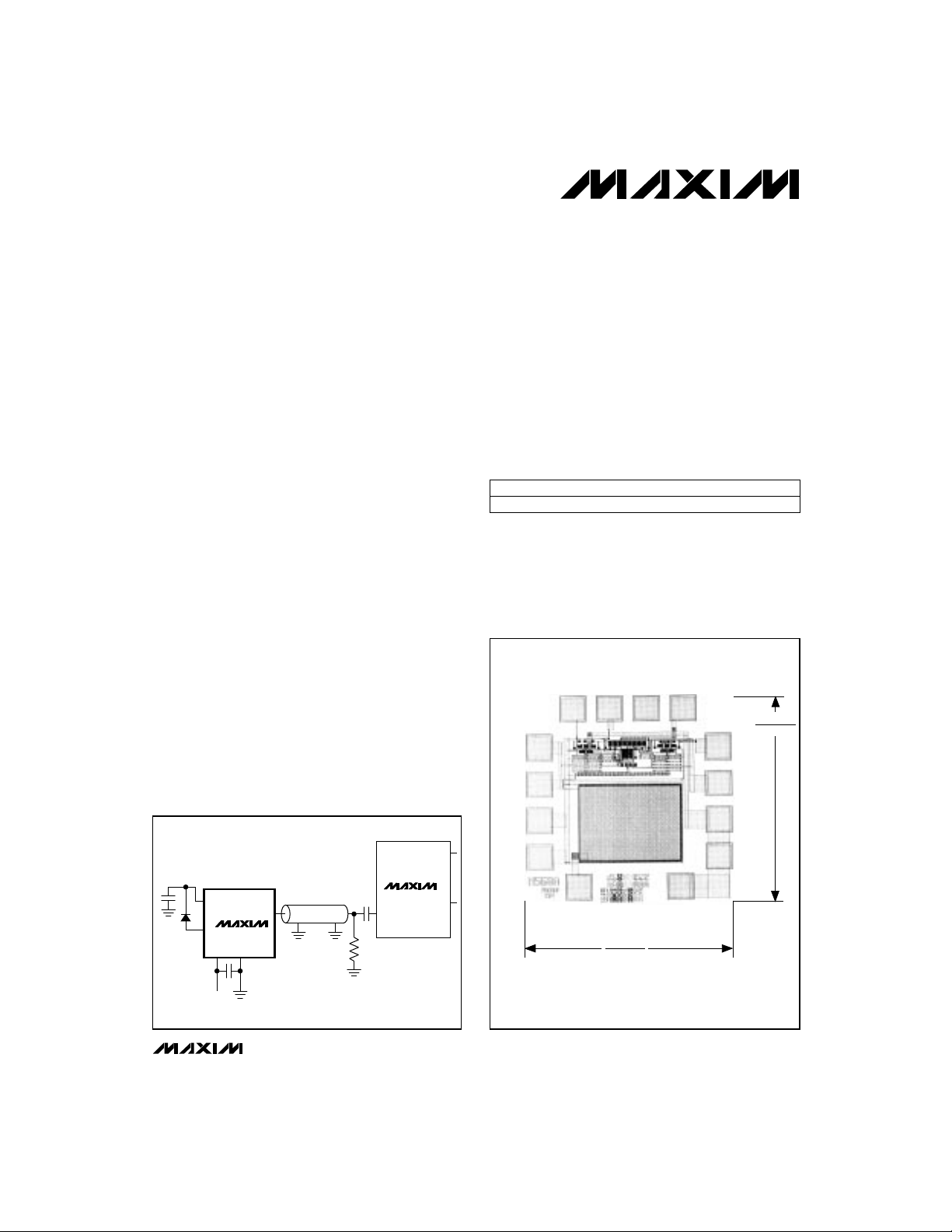
___________________Chip Topography
I
FILTER N.C. V
IN
14 13 12 11
1
V
B
CC
OUT
(1.016mm)
GND
10
0.040"
MAX3260
2
VCCB
__________Typical Operating Circuit
3
V
A
CC
DOUT+
LIMITING
AMPLIFIER
50Ω
DIN-
MAX3262
DOUT-
FILTER
V
I
IN
MAX3260
VCCGND
+5V
________________________________________________________________
Zo = 50Ω
OUT
V
A
4
CC
N.C.
0.040"
(1.016mm)
TRANSISTOR COUNT: 16
SUBSTRATE CONNECTED TO GND
Maxim Integrated Products
Call toll free 1-800-998-8800 for free samples or literature.
GND
GND
9
GND
8
7
GND
65
1
Page 2
1GHz Transimpedance Preamplifier
with 25dB Dynamic Range
ABSOLUTE MAXIMUM RATINGS
Supply Voltage, V
Input Current, I
Input Bias Voltage, V
Stresses beyond those listed under “Absolute Maximum Ratings” may cause permanent damage to the device. These are stress ratings only, and functional
operation of the device at these or any other conditions beyond those indicated in the operational sections of the specifications is not implied. Exposure to
absolute maximum rating conditions for extended periods may affect device reliability.
ELECTRICAL CHARACTERISTICS
MAX3260
(VCC= +5V, output terminated with 50Ω to ground, 100% tested, TJ= +27°C, unless otherwise noted.)
A, VCCB to GND ...............................0V, 6V
CC
, FILTER..................................................1.5mA
IN
......................................................0V, 6V
IN
DC SPECIFICATIONS
Input Bias Voltage
DC-Restore Time Constant
Filter Resistor Value
Supply Current
DC Transimpedance
DC-Restore Activation Current
IN
DC
FILTER
VCC
RESTORE
50Ω load to ground
IIN> 400µA
IIN< 100µA
AC SPECIFICATIONS (Not production tested)
Peak Input Current
IN
(Notes 1, 2, 3) ps100PWDPulse-Width Distortion
Input Referred Current Noise
RMS
(Notes 2, 4) nA240IN
Note 1: Input is a square wave with 0.5GHz frequency and <200ps rise time.
Note 2: External capacitance on the input ≤ 0.4pF.
Note 3: Pulse-width distortion measured at the 50% level of the output pulses: Input is 900µA, zero-peak.
Note 4: Output noise is measured through a four-pole Bessel filter with -3dB bandwidth of 800MHz.
Noise is then referred to the input by dividing the DC transimpedance.
Output Voltage, V
Operating Junction Temperature Range...........-55°C to +150°C
........................................................0V, 6V
OUT
Processing Temperature..................................................+400°C
CONDITIONS
CONDITIONS UNITSMIN TYP MAXSYMBOLPARAMETER
-400
-2400 -2000 -1600
UNITSMIN TYP MAXSYMBOLPARAMETER
V1.6V
µs1t
Ω750 1250R
mA56 70I
V/A
µA350I
V/A-2400 -2000 -1600GTSmall-Signal Transimpedance
GHz0.8 1.0BWU-3dB Bandwidth
µA900I
dB21PSRRPower-Supply Rejection Ratio
Ω3ROUTOutput Resistance
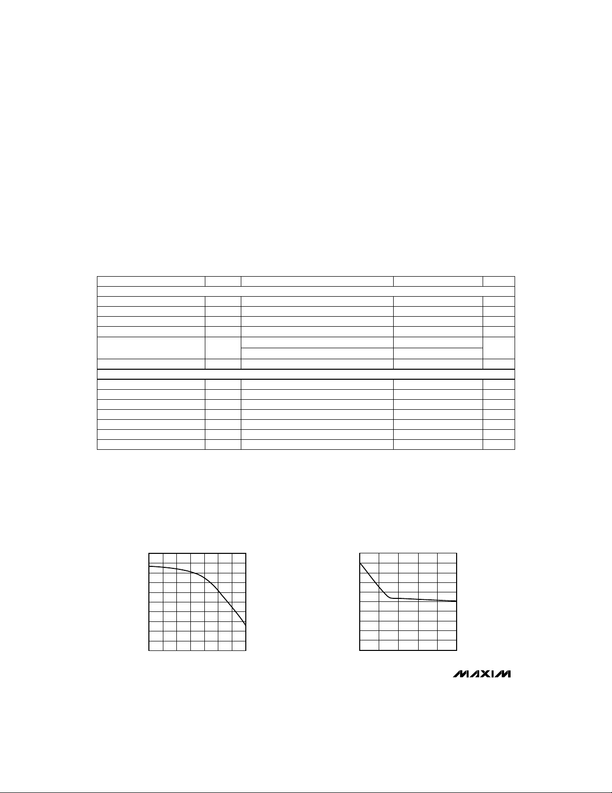
__________________________________________Typical Operating Characteristics
(TJ = +27°C, unless otherwise noted.)
FREQUENCY RESPONSE
68
67
66
65
64
63
GAIN (dB)
IN
/I
62
OUT
V
61
60
59
58
0
200 400 600 800 1000 14001200
FREQUENCY (MHz)
MAX3260-01
2.0
1.8
1.6
1.4
1.2
(V)
1.0
OUT
V
0.8
0.6
0.4
0.2
DC TRANSFER FUNCTION
0
0
200 400 1000
2 _______________________________________________________________________________________
IIN (µA)
600
MAX3260-03
800
Page 3

1GHz Transimpedance Preamplifier
with 25dB Dynamic Range
____________________________Typical Operating Characteristics (continued)
(TJ = +27°C, unless otherwise noted.)
2.0905V
100mV/div
1.0905V
37.98ns
_______________Detailed Description
The MAX3260 is a high-speed transimpedance amplifier, designed to accomodate input currents with a large
dynamic range. This circuit is optimized to operate in a
1062Mbps Fibre Channel reciever, and is also suitable
for use in 622Mbps SONET applications.
The MAX3260 employs shunt-shunt feedback around a
bipolar amplifier. The resulting circuit provides an
inverted current-to-voltage conversion. The conversion
gain is nominally -2000V/A.
Modern fiber-optic communications systems place
many requirements on transimpedance preamplifiers.
Power budgets are important when considering a preamp, since the circuit will generally be placed into a
small module or header, which limits the amount of heat
dissipation. In addition, the signal presented to the preamp may carry an 18dB to 20dB dynamic range, which
must be amplified linearly to prevent the addition of jitter. Finally, preamp noise generally determines the
receiver sensitivity, and must be held to a minimum.
The MAX3260 employs several techniques to address
the needs of fiber-optic preamplifiers. The output of the
MAX3260 operates in the 1V to 2V range (depending
EYE DIAGRAM
1Gbps
250ps/div
40.48ns
MAX3260-4
SUPPLY CURRENT vs. TEMPERATURE
(OUTPUT AC COUPLED)
30
28
26
24
22
20
18
SUPPLY CUREENT (mA)
16
14
5.25V
0
20 40 60 80 100
TEMPERATURE (°C)
5.0V
4.75V
MAX3260-TOC5
on the average input) to keep output standing current
at a minimum. The reduced output voltage helps keep
power consumption low, but also reduces the dynamic
range of the output stage. Fiber communications transimpedance amplifiers commonly use dynamic control
of the shunt-shunt feedback loop to vary the gain. The
unwanted side-effect of this technique is a circuit bandwidth that varies with input current. To prevent outputstage saturation, the MAX3260 employs a DC-restore
circuit. As input signal power increases, DC current is
drawn away from the input node of the amplifier. This
reduces the DC gain of the amplifier without affecting
the small-signal performance. To prevent noise feedback at low signals, an integrated comparator senses
the power level and disables the DC-restore function.
The MAX3260’s filter output provides a convenient voltage source for a photodiode, especially when the circuit
will be placed into a TO-style header with the photodiode. The filter output is connected to VCCthrough an
on-chip 1kΩ resistor. In combination with a bypass
capacitor, the filter function reduces the bandwidth at
the anode of the photodiode, therefore significantly
reducing the amount of noise at the cathode. The filter
connection can be left unconnected if not used.
MAX3260
_______________________________________________________________________________________
3
Page 4

1GHz Transimpedance Preamplifier
with 25dB Dynamic Range
VCCA
1k
FILTER
2.5k
MAX3260
Figure 1. Functional Diagram
I
IN
1.6V
MAX3260
A
V
CC
_______________________Wire Bonding
For high current density and reliable operation, the
MAX3260 uses gold metallization. Connections to the
die should be made with gold wire only, using ball
bonding techniques. Wegde bonding is not recommended. Die pad size is 4 mils.
__________________Design Procedure
The MAX3260 is a high-speed, high-gain component.
Its performance is strongly affected by module design
and layout. Improper design techniques can cause
oscillations or ringing.
In fiber-optic receiver applications, it is highly recommended that the transimpedance preamplifier be
placed close to the photodetector, in the same package or header if possible. This reduces parasitic inductance and improves static-discharge protection during
manufacturing. An alternative layout is to assemble the
preamplifier on a hybrid circuit board. In either case,
the designer should ensure that power-supply runs to
the VCCA and VCCB inputs are properly filtered. Keep
ground connections to the MAX3260 short and minimize inductance. Multiple vias may be required when
connecting to the ground plane on a circuit board, to
reduce the ground inductance.
VCCB
V
OUT
4k
V
A
CC
COMPARATOR
DC RESTORE
CIRCUIT
The MAX3260 will typically be connected to a limiting
or post amplifier by means of a controlled-impedance
transmission line. If a transmission line is used, it is
important to end-terminate the line with the characteristic impedance to prevent reflections into the output of
the MAX3260.
__________Applications Information
The MAX3260 consumes approximately 23mA of current with no output load. Typically, the majority of power
used by the preamplifier is consumed in the output termination. The termination is needed at the end of the
transmission line connecting MAX3260 to a limiting
amplifer. The average output level is typically 1.6V, and
is maintained at that level by the DC-restore function. A
50Ω termination to ground will consume 32mA of standing current. Power consumption can be reduced by terminating to higher resistance. A 75Ω transmission line
and termination would consume only 22mA. Power consumption can be reduced dramatically by excluding
the transmission line and termination, which requires
very short distances between the MAX3260 and the following circuit.
Maxim cannot assume responsibility for use of any circuitry other than circuitry entirely embodied in a Maxim product. No circuit patent licenses are
implied. Maxim reserves the right to change the circuitry and specifications without notice at any time.
4
___________________Maxim Integrated Products, 120 San Gabriel Drive, Sunnyvale, CA 94086 (408) 737-7600
© 1994 Maxim Integrated Products Printed USA is a registered trademark of Maxim Integrated Products.
 Loading...