

Page 1
现货库存、技术资料、百科信息、热点资讯,精彩尽在鼎好!
General Description
The MAX3250 is a 3.0V to 5.5V powered, ±50V isolated
EIA/TIA-232 and V.28/V.24 communications interface
with high data-rate capabilities. The MAX3250 is a dual
die part that operates with up to ±50V difference
between the RS-232 side and the logic side (ISOCOM
to GND). This makes the device ideal for operation in
noisy conditions with high common-mode voltages.
This feature prevents damage to the device if RS-232
lines are inadvertently short-circuited to a +24V or ±48V
power bus.
The MAX3250 is powered by a single 3V to 5.5V supply
on the logic side. Power is transferred from the logic
side to the isolated side by ±100V external capacitors.
The MAX3250 has two receivers (Rx) and two drivers
(Tx) and is guaranteed to run at data rates of 250kbps
while maintaining RS-232 output levels. The transceivers have a proprietary low-dropout transmitter output stage, delivering true RS-232 performance from a
3V to 5.5V supply with a dual charge pump. The device
features a FAULT open-drain output to signal an excessive isolated-side voltage condition on any of the RS232 inputs. This output can drive an alarm LED or can
be monitored by the processor to prevent operation
under these conditions. The receiver outputs are high
impedance in shutdown, allowing multiple interfaces
(IrDA, RS-232, RS-485) to be connected to the same
UART.
The MAX3250 is available in a space-saving 28-pin
SSOP package.
Applications
Industrial Control
Programmable Logic Controller
Point-of-Sale Equipment
PC-to-Router Connections
Diagnostic Ports
Telecom Equipment
Features
♦ ±50V Isolation
♦ 20µA Supply Current in Shutdown
♦ 250kbps Guaranteed Data Rate
♦ FAULT Output
♦ High-Impedance Transmitter and Receiver
Outputs in Shutdown
♦ Space-Saving SSOP Package
♦ Inductorless/Transformerless Design Simplifies
EMI Compliance
♦ Low-Cost Replacement for Opto-Isolated
Transceivers
♦ Meets EIA/TIA-232 Specifications Down to 3.0V
MAX3250
±50V Isolated, 3.0V to 5.5V,
250kbps, 2 Tx/2 Rx, RS-232 Transceiver
________________________________________________________________ Maxim Integrated Products 1
Ordering Information
19-2443; Rev 1; 2/03
For pricing, delivery, and ordering information, please contact Maxim/Dallas Direct! at
1-888-629-4642, or visit Maxim’s website at www.maxim-ic.com.
Typical Operating Circuit appears at end of data sheet.
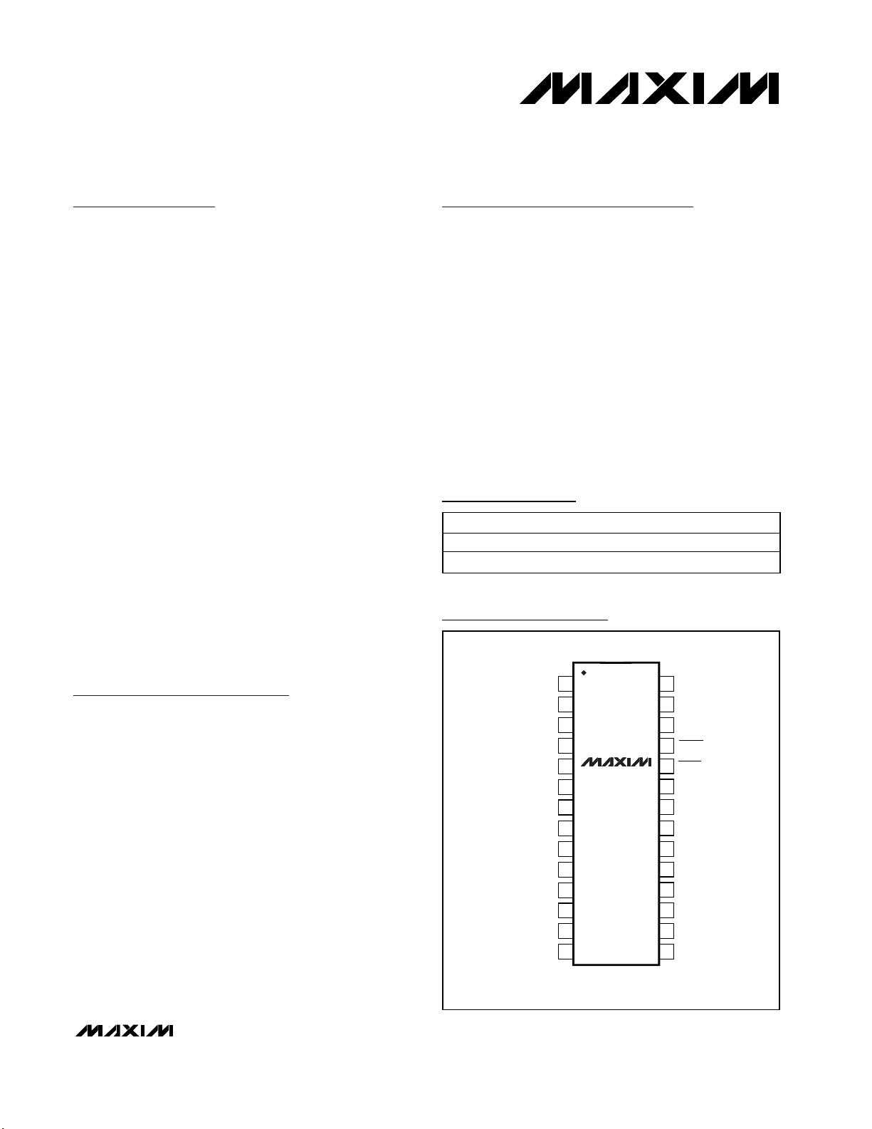
Pin Configuration
PART TEMP RANGE PIN-PACKAGE
MAX3250CAI 0°C to +70°C 28 SSOP
MAX3250EAI -40°C to +85°C 28 SSOP
TOP VIEW
C1-
R1OUT
R2OUT
T1IN
T2IN
N.C.
N.C.
C1+
C3+
C3-
C4+
C4-
1
2
3
4
5
MAX3250
6
7
8
9
10
V+
11
12
13
14
V-
SSOP
28
27
26
25
24
23
22
21
20
19
18
17
16
15
V
CC
C2-
GND
FAULT
SHDN
N.C.
N.C.
C2+
ISOV
CC
R1IN
R2IN
T1OUT
T2OUT
ISOCOM
Page 2
MAX3250
±50V Isolated, 3.0V to 5.5V,
250kbps, 2 TX/2 RX, RS-232 Transceiver
2 _______________________________________________________________________________________
ABSOLUTE MAXIMUM RATINGS
Stresses beyond those listed under “Absolute Maximum Ratings” may cause permanent damage to the device. These are stress ratings only, and functional
operation of the device at these or any other conditions beyond those indicated in the operational sections of the specifications is not implied. Exposure to
absolute maximum rating conditions for extended periods may affect device reliability.
All Voltages Referenced to GND, Unless Otherwise Noted.
V
CC
...........................................................................-0.3V to +6V
ISOCOM...............................................................................±80V
ISOV
CC
to ISOCOM..................................................-0.3V to +6V
V+ to ISOCOM (Note 1)............................................-0.3V to +7V
V- to ISOCOM (Note 1)............................................+0.3V to -7V
V+ + |V-| (Note 1) ...................................................................13V
Input Voltages
T_IN, SHDN ...........................................................-0.3V to +6V
R_IN to ISOCOM...............................................................±25V
Output Voltages
T_OUT to ISOCOM ........................................................±13.2V
R_OUT.....................................................-0.3V to (V
CC
+ 0.3V)
FAULT....................................................................-0.3V to +6V
C1-, C2-......................................................-0.3V to (V
CC
+ 0.3V)
C1+, C2+, C3+, C3-, C4+, C4-
to ISOCOM ......................................-0.3V to (ISOV
CC
+ 0.3V)
T_OUT Current ..............30mA (continuous), 50mA (peak, 10µs)
R_IN Current..................30mA (continuous), 50mA (peak, 10µs)
ISOCOM Current ...........30mA (continuous), 50mA (peak, 10µs)
Short-Circuit Duration T_OUT to ISOCOM .................Continuous
Continuous Power Dissipation (T
A
= +70°C)
28-Pin SSOP (derate 9.5mW/°C above +70°C) ...........762mW
Operating Temperature Ranges
MAX3250CAI .....................................................0°C to +70°C
MAX3250EAI...................................................-40°C to +85°C
Storage Temperature Range .............................-65°C to +150°C
Lead Temperature (soldering, 10s) .................................+300°C
ELECTRICAL CHARACTERISTICS
(VCC= 3.0V to 5.5V, see Typical Operating Circuit and Table 1 for capacitor values, ISOCOM = GND, TA= T
MIN
to T
MAX
, unless oth-
erwise noted. Typical values are at V
CC
= 3.3V and TA= +25°C.) (Note 2)
Note 1: V+ and V- can have a maximum magnitude of 7V, but their absolute difference cannot exceed 13V.
DC CHARACTERISTICS
Supply Current SHDN = VCC, no load 15 35 mA
Supply Current Shutdown
Maximum Ground Differential |V
Isolation Resistance Between GND and ISOCOM 60 kΩ
LOGIC INPUTS
Input Logic Low T_IN, SHDN 0.8 V
Input Logic High T_IN, SHDN
Transmitter Input Hysteresis 0.5 V
Input Leakage Current T_IN, SHDN -1 ±0.01 +1 µA
RECEIVER OUTPUTS
Output Leakage Current SHDN = GND -10 ±0.05 +10 µA
Output Voltage Low I
PARAMETER CONDITIONS MIN TYP MAX UNITS
SHDN = GND, V
SHDN = GND, V
- V
GND
ISOCOM
= 1.6mA 0.4 V
OUT
= GND 20 45
ISOCOM
= ±50V ±350
ISOCOM
| 50 V
V
= 3.3V 2.0
CC
V
= 5.0V 2.4
CC
µA
V
Output Voltage High I
FAULT OUTPUT
Output Voltage Low
(Open Drain)
Output Leakage Current FAULT not asserted 1 µA
FAULT Trip Level |V
= -1.0mA V
OUT
I
= 5mA 0.4 V
OUT
GND
- V
| 55 V
ISOCOM
CC
- 0.6 V
- 0.1 V
CC
Page 3
MAX3250
±50V Isolated, 3.0V to 5.5V,
250kbps, 2 TX/2 RX, RS-232 Transceiver
_______________________________________________________________________________________ 3
ELECTRICAL CHARACTERISTICS (continued)
(VCC= 3.0V to 5.5V, see Typical Operating Circuit and Table 1 for capacitor values, ISOCOM = GND, TA= T
MIN
to T
MAX
, unless oth-
erwise noted. Typical values are at V
CC
= 3.3V and TA= +25°C.) (Note 2)
PARAMETER CONDITIONS
UNITS
RECEIVER INPUTS (relative to ISOCOM)
Input Voltage Range -25
V
V
CC
= 3.3V 1.2 0.6
Input Threshold Low TA = +25°C
V
CC
= 5.0V 1.3 0.8
V
V
CC
= 3.3V 2.4 1.6
Input Threshold High TA = +25°C
V
CC
= 5.0V 2.4 1.7
V
Input Hysteresis 0.5 V
Input Resistance TA = +25°C 357kΩ
TRANSMITTER OUTPUTS (relative to ISOCOM)
Output Voltage Swing All transmitter outputs loaded with 3kΩ to ISOCOM
V
Output Resistance ISOVCC = V+ = V- = 0V, T_OUT = ±2V
Ω
Output Short-Circuit Current -60
mA
Output Leakage Current VCC = 0 or 3V to 5.5V, T_OUT = ±12V, SHDN = GND -25
µA
TIMING CHARACTERISTICS
(VCC= 3.0V to 5.5V, see Typical Operating Circuit and Table 1 for capacitor values, ISOCOM = GND, TA= T
MIN
to T
MAX
, unless oth-
erwise noted. Typical values are at V
CC
= 3.3V and TA= +25°C.)
Note 2: All currents into the device are positive; all currents out of the device are negative. All voltages are referenced to device
ground, unless otherwise noted.
Note 3: Transmitter skew is measured at the transmitter zero crosspoints.
MIN TYP MAX
±5.0 ±5.4
300 10M
+25
+60
+25
Maximum Data Rate
Receiver Propagation Delay R_IN to R_OUT, CL = 150pF to GND 0.4 µs
Receiver Skew |t
Transmitter Skew |t
Transition-Region Slew Rate
FAULT Propagation Delay 0.3 µs
Time to Shutdown 0.5 µs
Time to Exit Shutdown
PARAMETER CONDITIONS MIN TYP MAX UNITS
= 3kΩ, CL = 1000pF to ISOCOM, one transmitter
R
L
- t
PHL
PHL
V
CC
= 3kΩ to 7kΩ to ISOCOM,
R
L
measured from +3V to -3V or
-3V to +3V
V
ISOCOM
V
ISOCOM
| 100 ns
PLH
- t
| (Note 3) 120 ns
PLH
= 3.3V, TA = +25°C,
= GND 300
= ±50V 350
CL = 150pF to 1000pF
to ISOCOM
C
= 150pF to 2500pF
L
to ISOCOM
250 kbps
630
430
V/µs
µs
Page 4

MAX3250
±50V Isolated, 3.0V to 5.5V,
250kbps, 2 TX/2 RX, RS-232 Transceiver
4 _______________________________________________________________________________________
Typical Operating Characteristics
(VCC= 3.3V, 250kbps data rate, see Typical Operating Circuit and Table 1 for capacitor values, all transmitters loaded with 3kΩ and
C
L
to ISOCOM, TA= +25°C, unless otherwise noted.)
MAX3250 toc05
TEMPERATURE (°C)
SUPPLY CURRENT (µA)
603510-15
-200
-100
0
100
200
300
400
-300
-40 85
SHUTDOWN CURRENT
vs. TEMPERATURE
ISOCOM = -50V
ISOCOM = 0V
ISOCOM = +50V
TIME TO EXIT SHUTDOWN
V
ISOCOM
= 0V
TOUT
5V/div
MAX3250 toc04
100µs/div
SHDN
5V/div
MAX3250 toc03
LOAD CAPACITANCE (pF)
SUPPLY CURRENT (mA)
4000300020001000
10
20
30
40
50
60
70
80
90
0
0 5000
T1 TRANSMITTING AT 250kbps
T2 TRANSMITTING AT 20kbps
OPERATING SUPPLY CURRENT
vs. LOAD CAPACITANCE
250kbps
120kbps
20kbps
MAX3250 toc02
LOAD CAPACITANCE (pF)
SLEW RATE (V/µs)
4000300020001000
5
10
15
20
25
30
0
0 5000
SLEW RATE
vs. LOAD CAPACITANCE
-SLEW
+SLEW
FOR DATA RATES UP TO 250kbps
MAX3250 toc01
LOAD CAPACITANCE (pF)
TRANSMITTER OUTPUT VOLTAGE (V)
4000300020001000
-4
-2
0
2
4
6
8
-6
0 5000
TRANSMITTER OUTPUT VOLTAGE
vs. LOAD CAPACITANCE
V
OUT+
V
OUT-
T1 TRANSMITTING AT 250kbps
T2 TRANSMITTING AT 20kbps
COMMON-MODE FAULT RESPONSE
ISOCOM
50V/div
MAX3250 toc07
FAULT
5V/div
4ms/div
PEAK GROUND OFFSET VOLTAGE
vs. FREQUENCY
MAX3250 toc06
FREQUENCY (Hz)
PEAK GROUND OFFSET (±V)
300100 200 400 500
10
20
30
40
50
60
0
0 600
VCC = 3.3V
VCC = 5V
Page 5
MAX3250
±50V Isolated, 3.0V to 5.5V,
250kbps, 2 TX/2 RX, RS-232 Transceiver
_______________________________________________________________________________________ 5
Pin Description
PIN NAME FUNCTION
1 C1-
2 R1OUT TTL/CMOS Receiver Output
3 R2OUT TTL/CMOS Receiver Output
4 T1IN TTL/CMOS Transmitter Input
5 T2IN TTL/CMOS Transmitter Input
6, 22, 23 N.C. No Connection. Not internally connected.
7 N.C. No Connection. Leave unconnected or connect to ISOCOM.
8 C1+
9 C3+
10 V+
11 C3-
12 C4+
13 C4-
14 V-
15 ISOCOM Isolated Ground
16 T2OUT RS-232 Transmitter Output
17 T1OUT RS-232 Transmitter Output
18 R2IN RS-232 Receiver Input
19 R1IN RS-232 Receiver Input
20 ISOV
21 C2+
24 SHDN
25 FAULT Overvoltage Indicator. Active low, open drain.
26 GND Ground
27 C2-
28 V
CC
Negative Terminal of the Power Isolation Capacitor. Connect a 100V capacitor from C1- to C1+.
See Table 1 for values.
Positive Terminal of the Power Isolation Capacitor. Connect a 100V capacitor from C1+ to C1-.
See Table 1 for values.
Positive Terminal of the Voltage-Doubler Charge-Pump Capacitor. Connect a 0.1µF capacitor from
C3+ to C3-.
+5.5V Generated by the Charge Pump, Referenced to ISOCOM. Bypass V+ to ISOCOM with a
0.47µF capacitor.
Negative Terminal of the Voltage-Doubler Charge-Pump Capacitor. Connect a 0.1µF capacitor from
C3- to C3+.
Positive Terminal of the Inverting Charge-Pump Capacitor. Connect a 0.47µF capacitor from
C4+ to C4-.
Negative Terminal of the Inverting Charge-Pump Capacitor. Connect a 0.47µF capacitor from
C4- to C4+.
-5.5V Generated by the Charge Pump, Referenced to ISOCOM. Bypass V- to ISOCOM with a 0.47µF
capacitor.
Internally Generated Isolated Power-Supply Voltage, Referenced to ISOCOM. Bypass ISOVCC to
CC
ISOCOM with a 1µF capacitor.
Positive Terminal of the Power Isolation Capacitor. Connect a 100V capacitor from C2+ to C2-.
See Table 1 for values.
Shutdown Control. Drive SHDN low to enter low-power shutdown mode. Drive SHDN high or connect
to V
for normal operation.
CC
Negative Terminal of the Power Isolation Capacitor. Connect a 100V capacitor from C2- to C2+.
See Table 1 for values.
3.0V to 5.5V Supply Voltage. Bypass VCC to GND with a 1µF capacitor.
Page 6
MAX3250
±50V Isolated, 3.0V to 5.5V,
250kbps, 2 TX/2 RX, RS-232 Transceiver
6 _______________________________________________________________________________________
Detailed Description
The MAX3250 is a 3.0V to 5.5V powered, ±50V isolated
EIA/TIA-232 and V.28/V.24 communications interface
with high data-rate capabilities. The MAX3250 is a dual
die part that operates with up to ±50V difference
between the RS-232 side and the logic side (ISOCOM
to GND). This makes the device ideal for operation in
noisy conditions with high common-mode voltages.
This feature prevents damage to the device if RS-232
lines are inadvertently short-circuited to a +24V or ±48V
power bus.
The MAX3250 typically draws 15mA of supply current
when unloaded. Supply current drops to 20µA when
the device is placed in shutdown mode.
The MAX3250 has two receivers and two drivers and is
guaranteed to operate at data rates up to 250kbps. The
device features a FAULT open-drain output to signal an
excessive isolated-side voltage condition on any of the
RS-232 inputs. This output can drive an alarm LED or can
be monitored by the processor to prevent operation
under these conditions. The receiver outputs are high
impedance in shutdown, allowing multiple interfaces
(IrDA, RS-232, RS-485) to be connected to the same
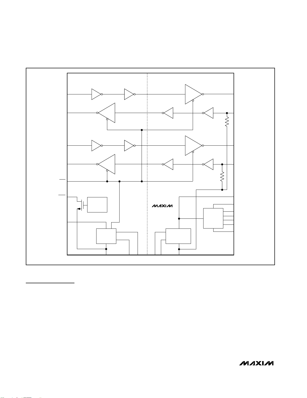
UART (Figure 1). The MAX3250 is a low-cost replacement
for opto-isolated transceivers.
Isolated Power Supply
The MAX3250 drives a high-frequency square wave into
C1 and a complementary square wave into C2. These
Figure 1. Functional Diagram
TIN1
ROUT1
TIN2
ROUT2
SHDN
FAULT
V
CC
OSC
FAULT
DETECTOR
MAX3250
POWER
CONTROLLER
RS-232
CHARGE
PUMP
TOUT1
RIN1
TOUT2
RIN2
ISOV
V+
C3+
C3-
C4+
C4-
V-
CC
GND C1- C2- C1+ C2+ ISOCOM
Page 7

MAX3250
±50V Isolated, 3.0V to 5.5V,
250kbps, 2 TX/2 RX, RS-232 Transceiver
_______________________________________________________________________________________ 7
AC waveforms are rectified on the isolated side of the
dual die to power its internal circuitry (ISOV
CC
).
Capacitor C6 filters the output of the rectifier. See the
Typical Operating Circuit.
The power controller works in a dual power mode. Power
is maximum when the isolated power supply is below its
regulation point. Power is reduced when the isolated
power supply is above its regulation point.
Dual Charge-Pump Voltage Converter
The RS-232 drivers are powered from a regulated dual
charge pump that provides output voltages of +5.5V (doubling charge pump) and -5.5V (inverting charge pump)
relative to ISOCOM over the 3.0V to 5.5V VCCrange.
The charge pumps are powered from ISOVCCand
operate in a discontinuous mode. If the output voltages
are less than 5.5V, the charge pumps are enabled. If
the output voltages exceed 5.5V, the charge pumps
are disabled. Each charge pump requires a flying
capacitor (C3, C4) and a reservoir capacitor (C7, C8)
to generate the V+ and V- supplies.
RS-232 Transmitters
The transmitters are inverting level translators that convert
TTL/CMOS-logic levels to ±5.0V EIA/TIA-232-compliant
levels. They guarantee a 250kbps data rate with worstcase loads of 3kΩ in parallel with 1000pF to ISOCOM. In
shutdown, the transmitters are disabled and the outputs
are forced into a high-impedance state. When powered
off or shut down, the outputs can be driven up to ±12V
relative to ISOCOM. The transmitter inputs do not have
pullup resistors. All unused inputs should be connected
to VCCor GND.
RS-232 Receivers
The receivers convert RS-232 signals to CMOS-logic
output levels. The receivers’ outputs are forced into a
high-impedance state when the device is in shutdown.
This allows a single UART to multiplex between different protocols.
Low-Power Shutdown Mode
Shutdown mode is obtained by driving SHDN low. In
shutdown, the devices typically draw only 20µA of supply current and no power is transferred across the isolation capacitors. The charge pumps are disabled, and
the receiver outputs and transmitter outputs are high
impedance. When exiting shutdown the charge pumps
and transmitter outputs are fully operational in typically
500µs (Figure 3). Connect SHDN to V
CC
if the shut-
down mode is not used.
Applications Information
Power Isolation Capacitors
The values for capacitors C1 and C2 are important for
proper operation of the device. These capacitors
should be 0.047µF for 4.5V to 5.5V operation, and
0.47µF for 3.0V to 3.6V operation. Smaller values result
in insufficient supply voltage on the isolated side.
Larger values are not allowed.
Capacitor C9 provides an AC feedback path for proper
controller operation. Connect C9 from ISOCOM to GND.
The values for C1, C2, and C9 determine the maximum
frequency and amplitude of the voltage difference
between the local and isolated ground. Table 1 shows
proper capacitance values.
Figure 2. Transmitter Output Voltage vs. Load Current per
Transmitter
Figure 3. Transmitter Outputs when Exiting Shutdown or
Powering Up
6
5
VCC = 3.0V
4
3
2
1
0
-1
-2
-3
-4
TRANSMITTER OUTPUT VOLTAGE (V)
-5
-6
T1
V
CC
T2
08
LOAD CURRENT PER TRANSMITTER (mA)
V
V
OUT1+
OUT2-
V
V
OUT+
OUT-
764 52 31
SHDN
5V/div
T1OUT
2V/div
VCC = 3.3V
100µs/div
T2OUT
Page 8

MAX3250
±50V Isolated, 3.0V to 5.5V,
250kbps, 2 TX/2 RX, RS-232 Transceiver
8 _______________________________________________________________________________________
To achieve full isolation capability, C1, C2, and C9
should be rated for 100V or higher operation and be X7R
or X5R type or metalized film dielectric. Y5V and Z5U
dielectrics should be avoided as their voltage and temperature coefficients make their power-transfer capabilities insufficient.
Charge-Pump and Bypass Capacitors
Capacitors C3–C8 should be X7R or X5R type dielectric. Their voltage rating needs to be 10V or higher.
Layout Information
Because the MAX3250 is intended for systems requiring ±50V isolation, some consideration in component
placement is necessary.
A 20mil air gap should isolate the logic side and the
isolated RS-232 side, across the N.C. pins (pin numbers 6, 7, 22, and 23) of the MAX3250. The only components that cross this air gap should be C1, C2, and
C9, which should all have a minimum 100V rating.
All capacitors should be located as close to the
MAX3250 as possible.
Maximum Voltage Between
ISOCOM and Logic GND
High values of applied isolation voltage and frequency
can cause ripple on ISOVCC, V+, V-, and in extreme
cases on VCC. Therefore, it is recommended that the
isolation-voltage and frequency be limited to the values
shown in the Typical Operating Characteristics.
Insert a 1kΩ 1/4W resistor in series with any isolation
test voltage when testing for maximum values of
applied isolation voltage. Exceeding the maximum limits of voltage and frequency (see the Typical Operating
Characteristics) could trigger a holding current in the
internal ESD-protection device if the ±80V isolation limit
is exceeded. This resistor should not be used in normal
application.
Transmitter Outputs when
Exiting Shutdown
Figure 3 shows two transmitter outputs when exiting
shutdown mode. As they become active, the two transmitter outputs are shown going to opposite RS-232 levels (one transmitter input is high, the other is low). Each
transmitter is loaded with 3kΩ in parallel with 2500pF.
The transmitter outputs display no ringing or undesirable transients as they come out of shutdown. Note that
the transmitters are enabled only when the magnitude
of V- exceeds approximately -3V.
Table 1. Required Capacitor Values
VCC (V) C1, C2 (µF) C3 (µF) C4, C7, C8 (µF) C5, C6 (µF) C9 (nF)
3.0 to 3.6 0.47 0.1 0.47 1 10
4.5 to 5.5 0.047 0.1 0.47 1 10
Page 9

MAX3250
±50V Isolated, 3.0V to 5.5V,
250kbps, 2 TX/2 RX, RS-232 Transceiver
_______________________________________________________________________________________ 9
Chip Information
TRANSISTOR COUNT: 2094
PROCESS: BiCMOS
RIN1
TOUT1
GND
V
CC
ISOCOM
V-
ISOV
CC
V+
RIN2
TOUT2
TIN1
ROUT1
TIN2
ROUT2
C1-
C1+
C2-
C2+
C4+
C4-
C3+
C3-
CABLE
V
CC
C5
1µF
C1
0.47µF
GND
OFFSET
REMOTE
GROUND
MAX3250
FAULT
SHDN
MICRO
C2
0.47µF
C9
10nF
±50V
C6
1µF
C8
0.47µFC70.47µF
C4
0.47µF
C3
0.1µF
REMOTE MICRO
REMOTE
XCVR
Typical Operating Circuit
Page 10

MAX3250
±50V Isolated, 3.0V to 5.5V,
250kbps, 2 TX/2 RX, RS-232 Transceiver
Maxim cannot assume responsibility for use of any circuitry other than circuitry entirely embodied in a Maxim product. No circuit patent licenses are
implied. Maxim reserves the right to change the circuitry and specifications without notice at any time.
10 ____________________Maxim Integrated Products, 120 San Gabriel Drive, Sunnyvale, CA 94086 408-737-7600
© 2003 Maxim Integrated Products Printed USA is a registered trademark of Maxim Integrated Products.
Package Information
(The package drawing(s) in this data sheet may not reflect the most current specifications. For the latest package outline information,
go to www.maxim-ic.com/packages
.)
e
NOTES:
1. D&E DO NOT INCLUDE MOLD FLASH.
2. MOLD FLASH OR PROTRUSIONS NOT TO EXCEED .15 MM (.006").
3. CONTROLLING DIMENSION: MILLIMETERS.
4. MEETS JEDEC MO150.
5. LEADS TO BE COPLANAR WITHIN 0.10 MM.
12
MAX
0.078
0.008
0.015
0.008
0.212
0.311
0.037
8∞
MILLIMETERS
MAX
MIN
1.73 1.99
0.21
0.05
0.38
0.25
0.20
0.09
5.20
5.38
0.65 BSC
7.90
7.65
0.63
0.95
0∞
8∞
INCHES
MIN
D
0.239
D
0.239
D
0.278
D
0.317
0.397
D
PROPRIETARY INFORMATION
TITLE:
MAX
0.249
0.249
0.289
0.328
0.407
MILLIMETERS
MAX
MIN
6.07
6.33
6.07
6.33
7.07
7.33
8.07
8.33
10.07
10.33
14L
16L
24L
28L
C
INCHES
DIM
MIN
A
0.068
A1
0.002
B
0.010
C
HE
N
A
B
A1
D
D
E
e
H
L
0.004
SEE VARIATIONS
0.205
0.0256 BSC
0.301
0.025
0∞
L
SSOP.EPS
N
20L
PACKAGE OUTLINE, SSOP, 5.3 MM
REV.DOCUMENT CONTROL NO.APPROVAL
21-0056
1
C
1
 Loading...