

For pricing, delivery, and ordering information, please contact Maxim Direct at 1-888-629-4642,
or visit Maxim's website at www.maxim-ic.com.
General Description
The MAX3222E/MAX3232E/MAX3237E/MAX3241E/
MAX3246E +3.0V-powered EIA/TIA-232 and V.28/V.24
communications interface devices feature low power consumption, high data-rate capabilities, and enhanced
electrostatic-discharge (ESD) protection. The enhanced
ESD structure protects all transmitter outputs and
receiver inputs to ±15kV using IEC 1000-4-2 Air-Gap
Discharge, ±8kV using IEC 1000-4-2 Contact Discharge
(±9kV for MAX3246E), and ±15kV using the Human Body
Model. The logic and receiver I/O pins of the MAX3237E
are protected to the above standards, while the transmitter output pins are protected to ±15kV using the Human
Body Model.
A proprietary low-dropout transmitter output stage delivers
true RS-232 performance from a +3.0V to +5.5V power
supply, using an internal dual charge pump. The charge
pump requires only four small 0.1µF capacitors for operation from a +3.3V supply. Each device guarantees operation at data rates of 250kbps while maintaining RS-232
output levels. The MAX3237E guarantees operation at
250kbps in the normal operating mode and 1Mbps in the
MegaBaud™ operating mode, while maintaining RS-232compliant output levels.
The MAX3222E/MAX3232E have two receivers and two
transmitters. The MAX3222E features a 1µA shutdown
mode that reduces power consumption in battery-powered portable systems. The MAX3222E receivers remain
active in shutdown mode, allowing monitoring of external
devices while consuming only 1µA of supply current. The
MAX3222E and MAX3232E are pin, package, and functionally compatible with the industry-standard MAX242
and MAX232, respectively.
The MAX3241E/MAX3246E are complete serial ports
(three drivers/five receivers) designed for notebook and
subnotebook computers. The MAX3237E (five drivers/
three receivers) is ideal for peripheral applications that
require fast data transfer. These devices feature a shutdown mode in which all receivers remain active, while
consuming only 1µA (MAX3241E/MAX3246E) or 10nA
(MAX3237E).
The MAX3222E, MAX3232E, and MAX3241E are available in space-saving SO, SSOP, TQFN and TSSOP packages. The MAX3237E is offered in an SSOP package.
The MAX3246E is offered in the ultra-small 6 x 6 UCSP™
package.
Next-Generation Device Features
♦♦
For Space-Constrained Applications
MAX3228E/MAX3229E: ±15kV ESD-Protected,
+2.5V to +5.5V, RS-232 Transceivers in UCSP
♦♦
For Low-Voltage or Data Cable Applications
MAX3380E/MAX3381E: +2.35V to +5.5V, 1µA,
2Tx/2Rx, RS-232 Transceivers with ±15kV
ESD-Protected I/O and Logic Pins
Applications
Battery-Powered Equipment
Cell Phones Smart Phones
Cell-Phone Data Cables
Notebook, Subnotebook, and Palmtop Computers
Printers
xDSL Modems
MAX3222E/MAX3232E/MAX3237E/MAX3241E /MAX3246E
±15kV ESD-Protected, Down to 10nA, 3.0V to 5.5V,
Up to 1Mbps, True RS-232 Transceivers
________________________________________________________________
Maxim Integrated Products
1
19-1298; Rev 12; 12/10
Ordering Information
Ordering Information continued at end of data sheet.
+
Denotes a lead(Pb)-free/RoHS-compliant package.
*
Dice are tested at TA= +25°C, DC parameters only.
**
EP = Exposed pad.
/V denotes an automotive qualified part.
Pin Configurations, Selector Guide, and Typical Operating
Circuits appear at end of data sheet.
MegaBaud and UCSP are trademarks of Maxim Integrated
Products, Inc.
PART TEMP RANGE PIN-PACKAGE
MAX3222ECTP+ 0°C to +70°C
MAX3222ECUP+ 0°C to +70°C 20 TSSOP
MAX3222ECAP+ 0°C to +70°C 20 SSOP
MAX3222ECWN+ 0°C to +70°C 18 Wide SO
MAX3222ECPN+ 0°C to +70°C 18 Plast ic DIP
MAX3222EC/D+ 0°C to +70°C Dice*
MAX3222EETP+ -40°C to +85°C
MAX3222EEUP/V+ -40°C to +85°C 20 TSSOP
MAX3222EEUP+ -40°C to +85°C 20 TSSOP
MAX3222EEAP+ -40°C to +85°C 20 SSOP
MAX3222EEWN+ -40°C to +85°C 18 Wide SO
MAX3222EEPN+ -40°C to +85°C 18 Plast ic DIP
MAX3232ECAE+ 0°C to +70°C 16 SSOP
MAX3232ECWE+ 0°C to +70°C 16 Wide SO
MAX3232ECPE+ 0°C to +70°C 16 Plastic DIP
20 TQFN-EP**
(5mm x 5mm)
20 TQFN-EP**
(5mm x 5mm)
MAX3222E/MAX3232E/MAX3237E/MAX3241E /MAX3246E
±15kV ESD-Protected, Down to 10nA, 3.0V to 5.5V,
Up to 1Mbps, True RS-232 Transceivers
2 _______________________________________________________________________________________
ABSOLUTE MAXIMUM RATINGS
ELECTRICAL CHARACTERISTICS
(VCC= +3V to +5.5V, C1–C4 = 0.1µF, TA= T
MIN
to T
MAX
, unless otherwise noted. Typical values are at TA= +25°C.) (Notes 3, 4)
Stresses beyond those listed under “Absolute Maximum Ratings” may cause permanent damage to the device. These are stress ratings only, and functional
operation of the device at these or any other conditions beyond those indicated in the operational sections of the specifications is not implied. Exposure to
absolute maximum rating conditions for extended periods may affect device reliability.
VCCto GND..............................................................-0.3V to +6V
V+ to GND (Note 1) ..................................................-0.3V to +7V
V- to GND (Note 1) ...................................................+0.3V to -7V
V+ + |V-| (Note 1).................................................................+13V
Input Voltages
T_IN, EN, SHDN, MBAUD to GND ........................-0.3V to +6V
R_IN to GND .....................................................................±25V
Output Voltages
T_OUT to GND...............................................................±13.2V
R_OUT, R_OUTB (MAX3237E/MAX3241E)...-0.3V to (V
CC
+ 0.3V)
Short-Circuit Duration, T_OUT to GND.......................Continuous
Continuous Power Dissipation (T
A
= +70°C)
16-Pin SSOP (derate 7.14mW/°C above +70°C) ..........571mW
16-Pin TSSOP (derate 9.4mW/°C above +70°C) .......754.7mW
16-Pin TQFN (derate 20.8mW/°C above +70°C) .....1666.7mW
16-Pin Wide SO (derate 9.52mW/°C above +70°C) .....762mW
18-Pin Wide SO (derate 9.52mW/°C above +70°C) .....762mW
18-Pin PDIP (derate 11.11mW/°C above +70°C)..........889mW
20-Pin TQFN (derate 21.3mW/°C above +70°C) ........1702mW
20-Pin TSSOP (derate 10.9mW/°C above +70°C) ........879mW
20-Pin SSOP (derate 8.00mW/°C above +70°C) ..........640mW
28-Pin SSOP (derate 9.52mW/°C above +70°C) ..........762mW
28-Pin Wide SO (derate 12.50mW/°C above +70°C) .............1W
28-Pin TSSOP (derate 12.8mW/°C above +70°C) ......1026mW
32-Pin TQFN (derate 33.3mW/°C above +70°C)...........2666mW
6 x 6 UCSP (derate 12.6mW/°C above +70°C) .............1010mW
Operating Temperature Ranges
MAX32_ _EC_ _ ...................................................0°C to +70°C
MAX32_ _EE_ _.................................................-40°C to +85°C
Storage Temperature Range .............................-65°C to +150°C
Lead Temperature (soldering, 10s) .................................+300°C
Soldering Temperature (reflow) .......................................+260°C
Bump Reflow Temperature (Note 2)
Infrared, 15s..................................................................+200°C
Vapor Phase, 20s..........................................................+215°C
Note 1: V+ and V- can have maximum magnitudes of 7V, but their absolute difference cannot exceed 13V.
Note 2: This device is constructed using a unique set of packaging techniques that impose a limit on the thermal profile the device
can be exposed to during board-level solder attach and rework. This limit permits only the use of the solder profiles recommended in the industry-standard specification, JEDEC 020A, paragraph 7.6, Table 3 for IR/VPR and convection reflow.
Preheating is required. Hand or wave soldering is not allowed.
DC CHARACTERISTICS (VCC = +3.3V or +5V, TA = +25°C)
Supply Current SHDN = VCC, no load
Shutdown Supply Current
LOGI C I N PUT S
Input Logic Low T_IN, EN, SHDN, MBAUD 0.8 V
Input Logic High T_IN, EN, SHDN, MBAUD
Transm itter Input Hysteresis 0.5 V
Input Leakage Current
PARAMETER CONDITIONS MIN TYP MAX UNITS
SHDN = GND 1 10 μA
SHDN = R_IN = GND, T_IN = GND or V
T_IN, EN, SHDN
T_IN, SHDN, MBAUD MAX3237E (Note 5) 9 18
MAX3222E, MAX3232E,
MAX3241E, MAX3246E
MAX3237E 0.5 2.0
(MAX3237E) 10 300 nA
CC
VCC = +3.3V 2.0
= +5.0V 2.4
V
CC
MAX3222E, MAX3232E,
MAX3241E, MAX3246E
0.3 1
±0.01 ±1
mA
V
μA
MAX3222E/MAX3232E/MAX3237E/MAX3241E /MAX3246E
±15kV ESD-Protected, Down to 10nA, 3.0V to 5.5V,
Up to 1Mbps, True RS-232 Transceivers
_______________________________________________________________________________________ 3
ELECTRICAL CHARACTERISTICS (continued)
(VCC= +3V to +5.5V, C1–C4 = 0.1µF, TA= T
MIN
to T
MAX
, unless otherwise noted. Typical values are at TA= +25°C.) (Notes 3, 4)
PARAMETER CONDITIONS MIN TYP MAX UNITS
RECEIVER OUTPUTS
Output Leakage Current
Output-Voltage Low
Output-Voltage High I
RECEIVER INPUTS
Input Voltage Range -25 +25 V
Input Threshold Low TA = +25°C
Input Threshold High TA = +25°C
Input Hysteresis 0.5 V
Input Resistance TA = +25°C 3 5 7 k
TRANSMITTER OUTPUTS
Output Voltage Swing
Output Resistance VCC = 0V, transmitter output = ±2V 300 50k
Output Short-Circuit Current ±60 mA
Output Leakage Current
MOUSE DRIVABILITY (MAX3241E)
Transm itter Output Voltage
ESD PROTECTION
R_IN, T_OUT
T_IN, R_IN, R_OUT, EN, SHDN,
MBAUD
R_OUT (MAX3222E/MAX3237E/MAX3241E/
MAX3246E), EN = V
I
OUT
MAX3246E), I
OUT
All transm itter output s loaded with 3 k to ground
(Note 6)
V
CC
disabled (MAX3222E/MAX3232E/MAX3241E/MAX3246E)
T1IN = T2IN = GND, T3IN = V
3k to GND, T1OUT and T2OUT loaded with 2.5mA
each
Human Body Model ±15
IEC 1000-4-2 Air-Gap Discharge (except MAX3237E) ±15
IEC 1000-4-2 Contact Discharge (except MAX3237E) ±8
IEC 1000-4-2 Contact Discharge (MAX3246E on ly) ±9
MAX3237E
= 1.6mA (MAX3222E/MAX3232E/MAX3241E/
= -1.0mA
= 0V or +3.0V to +5.5V, V
, receivers disab led
CC
= 1.0mA (MAX3237E)
OUT
VCC = +3.3V 0.6 1.1
= +5.0V 0.8 1.5
V
CC
VCC = +3.3V 1.5 2.4
= +5.0V 2.0 2.4
V
CC
= ±12V, transmitters
OUT
, T3OUT loaded with
CC
Human Body Model ±15
IEC 1000-4-2 Air-Gap Discharge ±15
IEC 1000-4-2 Contact Discharge ±8
±0.05 ±10 μA
0.4 V
V
-
CC
0.6
±5 ±5.4 V
±5 V
VCC -
0.1
±25 μA
V
V
V
kV
kV
MAX3222E/MAX3232E/MAX3237E/MAX3241E /MAX3246E
±15kV ESD-Protected, Down to 10nA, 3.0V to 5.5V,
Up to 1Mbps, True RS-232 Transceivers
4 _______________________________________________________________________________________
TIMING CHARACTERISTICS—MAX3237E
(VCC= +3V to +5.5V, C1–C4 = 0.1µF, TA= T
MIN
to T
MAX
, unless otherwise noted. Typical values are at TA= +25°C.) (Note 3)
Note 3: MAX3222E/MAX3232E/MAX3241E: C1–C4 = 0.1µF tested at +3.3V ±10%; C1 = 0.047µF, C2, C3, C4 = 0.33µF tested at +5.0V
±10%. MAX3237E: C1–C4 = 0.1µF tested at +3.3V ±5%, C1–C4 = 0.22µF tested at +3.3V ±10%; C1 = 0.047µF, C2, C3, C4 =
0.33µF tested at +5.0V ±10%. MAX3246E: C1-C4 = 0.22µF tested at +3.3V ±10%; C1 = 0.22µF, C2, C3, C4 = 0.54µF tested at
+5.0V ±10%.
Note 4: MAX3246E devices are production tested at +25°C. All limits are guaranteed by design over the operating temperature range.
Note 5: The MAX3237E logic inputs have an active positive feedback resistor. The input current goes to zero when the inputs are at
the supply rails.
Note 6: MAX3241EEUI is specified at T
A
= +25°C.
Note 7: Transmitter skew is measured at the transmitter zero crosspoints.
TIMING CHARACTERISTICS—MAX3222E/MAX3232E/MAX3241E/MAX3246E
(VCC= +3V to +5.5V, C1–C4 = 0.1µF, TA= T
MIN
to T
MAX
, unless otherwise noted. Typical values are at TA= +25°C.) (Notes 3, 4)
PARAMETER SYMBOL CONDITIONS MIN TYP MAX UNITS
Maximum Data Rate
Receiver Propagation Delay
Receiver Output Enable Time Normal operation (except MAX3232E) 200 ns
Receiver Output Disable Time Normal operation (except MAX3232E) 200 ns
Transmitter Skew |t
Receiver Skew |t
PHL
PHL
Transition-Region Slew Rate
Receiver Propagation Delay R_IN to R_OUT, CL = 150pF
Receiver Output Enable Time Normal operation 2.6 µs
Receiver Output Disable Time Normal operation 2.4 µs
Transmitter Skew (Note 7)
Receiver Skew |t
PARAMETER CONDITIONS MIN TYP MAX UNITS
RL = 3kΩ, CL = 1000pF, one transmitter switching,
MBAUD = GND
VCC = +3.0V to +4.5V, RL = 3kΩ, CL = 250pF,
one transmitter switching, MBAUD = V
V
CC
one transmitter switching, MBAUD = V
|t
PHL
|t
PHL
PHL
= 3kΩ,
R
L
C
= 1000pF,
L
one transmitter
switching T
TA = T
(MAX3222E/MAX3232E/
MAX3241E) (Note 6)
A
Receiver input to receiver output,
= 150pF
C
L
to T
MIN
MAX
250
= + 25°C ( M AX 3246E ) 250
0.15
0.15
kbps
µs
| (Note 7) 100 ns
|50ns
= + 3.3V , TA = + 25°C ,
V
C C
R
= 3kΩ to 7kΩ , m easur ed
L
fr om + 3.0V to - 3.0V or - 3.0V to
C
= 150pF
L
to 1000pF
6 30 V/µs
t
t
PHL
PLH
- t
- t
PLH
PLH
+ 3.0V , one tr ansm i tter sw i tchi ng
250
CC
= +4.5V to +5.5V, RL = 3kΩ, CL = 1000pF,
CC
t
PHL
t
PLH
- t
|, MBAUD = GND
PLH
- t
|, MBAUD = V
PLH
- t
|50ns
PLH
CC
1000Maximum Data Rate
1000
0.15
0.15
100 ns
kbps
µs
Transition-Region Slew Rate
VCC = +3.3V,
R
= 3kΩ to 7kΩ,
L
+3.0V to -3.0V or
-3.0V to +3.0V,
= +25°C
T
A
CL = 150pF
to 1000pF
C
= 150pF to 2500pF,
L
MBAUD = GND
MBAUD = GND 6 30
MBAUD = V
CC
24 150
430
V/µs
MAX3222E/MAX3232E/MAX3237E/MAX3241E /MAX3246E
±15kV ESD-Protected, Down to 10nA, 3.0V to 5.5V,
Up to 1Mbps, True RS-232 Transceivers
_______________________________________________________________________________________
5
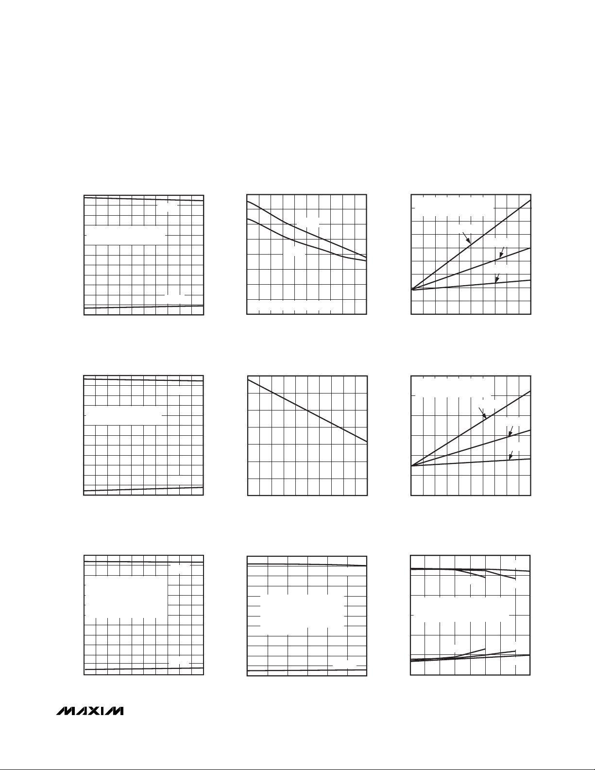
__________________________________________Typical Operating Characteristics
(VCC= +3.3V, 250kbps data rate, 0.1µF capacitors, all transmitters loaded with 3kΩ and CL, TA = +25°C, unless otherwise noted.)
MAX3222E/MAX3232E
TRANSMITTER OUTPUT VOLTAGE
vs. LOAD CAPACITANCE
6
5
4
3
T1 TRANSMITTING AT 250kbps
2
T2 TRANSMITTING AT 15.6kbps
1
0
-1
-2
-3
-4
TRANSMITTER OUTPUT VOLTAGE (V)
-5
-6
0 1000 2000 3000 4000 5000
LOAD CAPACITANCE (pF)
V
OUT+
16
14
MAX3237E toc01
12
10
8
6
SLEW RATE (V/μs)
4
V
OUT-
2
0
MAX3222E/MAX3232E
SLEW RATE vs. LOAD CAPACITANCE
-SLEW
+SLEW
FOR DATA RATES UP TO 250kbps
0 1000 2000 3000 4000 5000
LOAD CAPACITANCE (pF)
45
40
MAX3237E toc02
35
30
25
20
15
SUPPLY CURRENT (mA)
10
5
0
MAX3241E
TRANSMITTER OUTPUT VOLTAGE
vs. LOAD CAPACITANCE
6
5
4
3
1 TRANSMITTER AT 250kbps
2
2 TRANSMITTERS AT 15.6kbps
1
0
-1
-2
-3
-4
TRANSMITTER OUTPUT VOLTAGE (V)
-5
-6
0 1000 2000 3000 4000 5000
LOAD CAPACITANCE (pF)
MAX3237E
TRANSMITTER OUTPUT VOLTAGE
vs. LOAD CAPACITANCE (MBAUD = GND)
6
5
4
FOR DATA RATES UP TO 250kbps
3
1 TRANSMITTER AT 250kbps
2
4 TRANSMITTERS AT 15.6kbps
ALL TRANSMITTERS LOADED
1
WITH 3kΩ + C
0
-1
-2
-3
-4
TRANSMITTER OUTPUT VOLTAGE (V)
-5
-6
0
L
1000 1500500 2000 2500 3000
LOAD CAPACITANCE (pF)
SLEW RATE vs. LOAD CAPACITANCE
14
V
OUT+
V
OUT-
MAX3237E to04
12
10
8
6
SLEW RATE (V/μs)
4
2
0
0 1000 2000 3000 4000 5000
TRANSMITTER OUTPUT VOLTAGE
6
V
V
OUT+
OUT-
MAX3237E toc07
5
4
3
2
1
0
-1
-2
-3
-4
TRANSMITTER OUTPUT VOLTAGE (V)
-5
-6
0 1000 1500500 2000 2500 3000
MAX3241E
LOAD CAPACITANCE (pF)
MAX3237E
vs. LOAD CAPACITANCE
FOR DATA RATES UP TO 250kbps
1 TRANSMITTER 250kbps
4 TRANSMITTERS 15.6kbps
ALL TRANSMITTERS LOADED
WITH 3kΩ + C
L
LOAD CAPACITANCE (pF)
60
50
MAX3237E toc05
40
30
20
SUPPLY CURRENT (mA)
10
0
7.5
V
+
OUT
V
OUT-
5.0
MAX3246E toc07A
2.5
0
-2.5
-5.0
TRANSMITTER OUTPUT VOLTAGE (V)
-7.5
MAX3222E/MAX3232E
OPERATING SUPPLY CURRENT
vs. LOAD CAPACITANCE
T1 TRANSMITTING AT 250kbps
T2 TRANSMITTING AT 15.6kbps
250kbps
120kbps
20kbps
0 20001000 3000 4000 5000
LOAD CAPACITANCE (pF)
MAX3241E
OPERATING SUPPLY CURRENT
vs. LOAD CAPACITANCE
1 TRANSMITTER AT 250kbps
2 TRANSMITTERS AT 15.6kbps
250kbps
120kbps
20kbps
0 20001000 3000 4000 5000
LOAD CAPACITANCE (pF)
MAX3237E
TRANSMITTER OUTPUT VOLTAGE
vs. LOAD CAPACITANCE (MBAUD = V
2Mbps
1 TRANSMITTER AT FULL DATA RATE
4 TRANSMITTERS AT 1/16 DATA RATE
LOAD, EACH OUTPUT
3kΩ + C
L
2Mbps
0
500 1000 1500 2000
LOAD CAPACITANCE (pF)
CC
1Mbps
1.5Mbps
1.5Mbps
1Mbps
)
MAX3237E toc03
MAX3237E toc06
MAX3237E toc08
MAX3222E/MAX3232E/MAX3237E/MAX3241E /MAX3246E
±15kV ESD-Protected, Down to 10nA, 3.0V to 5.5V,
Up to 1Mbps, True RS-232 Transceivers
6 _______________________________________________________________________________________
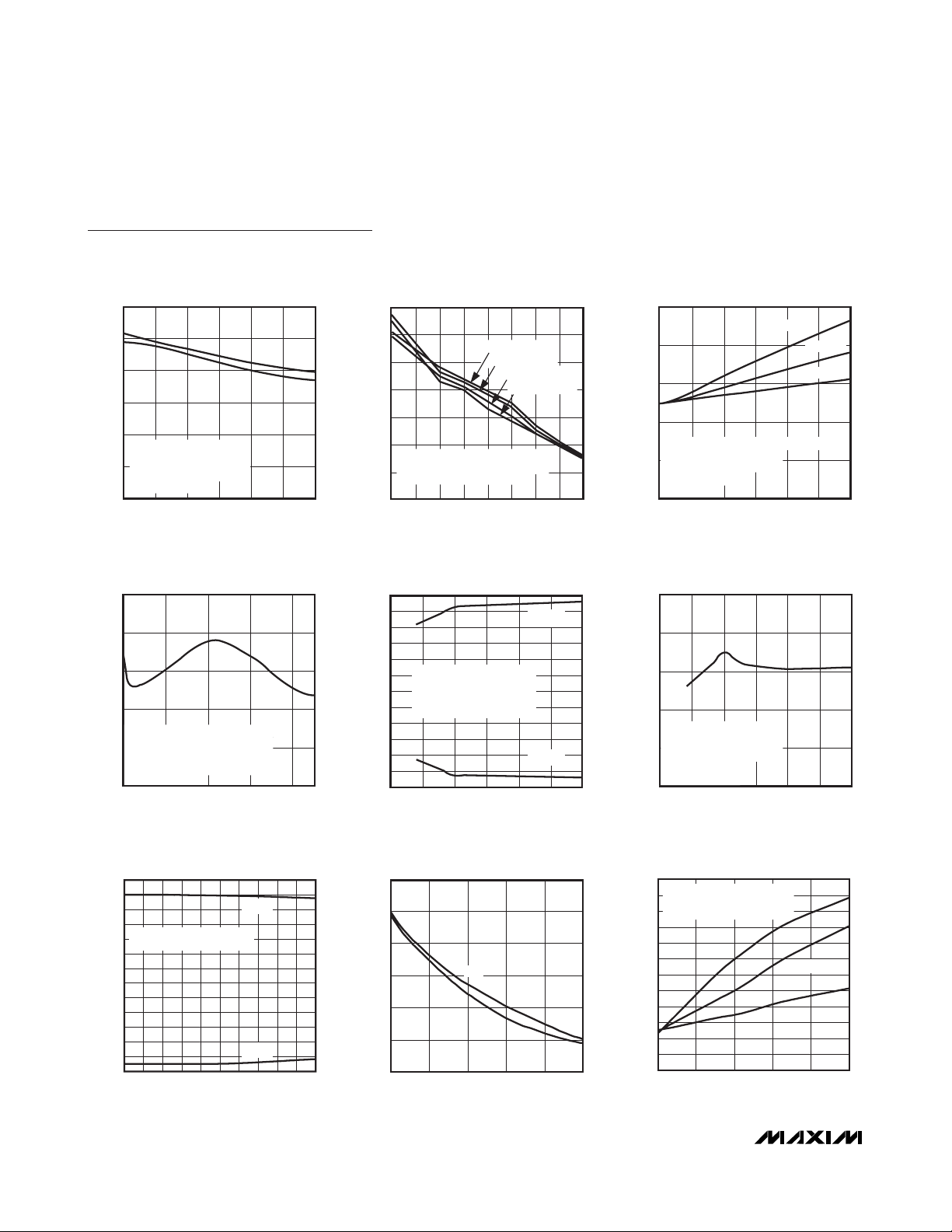
Typical Operating Characteristics (continued)
(VCC= +3.3V, 250kbps data rate, 0.1µF capacitors, all transmitters loaded with 3kΩ and CL, TA = +25°C, unless otherwise noted.)
SLEW RATE vs. LOAD CAPACITANCE
12
10
8
6
SLEW RATE (V/μs)
4
1 TRANSMITTER AT 250kbps
4 TRANSMITTERS AT 15.6kbps
2
ALL TRANSMITTERS LOADED
WITH 3kΩ + C
0
0
TRANSMITTER SKEW vs. LOAD CAPACITANCE
100
80
60
40
|t
- t
PLH
TRANSMITTER SKEW (ns)
1 TRANSMITTER AT 500kbps
20
4 TRANSMITTERS AT 1/16 DATA RATE
ALL TRANSMITTERS LOADED
WITH 3kΩ + C
0
0
TRANSMITTER OUTPUT VOLTAGE
7
6
5
4
1 TRANSMITTER AT 250kbps
3
2 TRANSMITTERS AT 15.6kbps
2
1
0
-1
-2
-3
TRANSMITTER OUTPUT VOLTAGE (V)
-4
-5
-6
0 5000
MAX3237E
(MBAUD = GND)
SR-
SR+
L
1000 1500500 2000 2500 3000
LOAD CAPACITANCE (pF)
MAX3237E
(MBAUD = V
|
PHL
L
1000 1500500 2000
LOAD CAPACITANCE (pF)
)
CC
MAX3246E
vs. LOAD CAPACITANCE
V
OUT+
V
OUT-
LOAD CAPACITANCE (pF)
MAX3237E
SUPPLY CURRENT vs. LOAD CAPACITANCE
WHEN TRANSMITTING DATA (MBAUD = GND)
50
40
30
20
SUPPLY CURRENT (mA)
1 TRANSMITTER AT 20kbps, 120kbps, 250kbps
4 TRANSMITTERS AT 15.6kbps
10
ALL TRANSMITTERS LOADED
WITH 3kΩ + C
0
0
MAX3237E toc09
SLEW RATE vs. LOAD CAPACITANCE
(MBAUD = V
70
60
50
40
30
SLEW RATE (V/μs)
20
1 TRANSMITTER AT FULL DATA RATE
4 TRANSMITTERS AT 1/16 DATA RATE
10
3kΩ + C
L
0
500 1000 1500 2000
0
-SLEW, 1Mbps
LOAD EACH OUTPUT
LOAD CAPACITANCE (pF)
)
CC
+SLEW, 1Mbps
-SLEW, 2Mbps
+SLEW, 2Mbps
MAX3237E toc10
MAX3237E
TRANSMITTER OUTPUT VOLTAGE
vs. SUPPLY VOLTAGE (MBAUD = GND)
6
MAX3237E toc12
5
4
3
2
1
0
-1
-2
-3
-4
TRANSMITTER OUTPUT VOLTAGE (V)
-5
-6
2.0 3.0 3.52.5 4.0 4.5 5.0
1 TRANSMITTER AT 250kbps
4 TRANSMITTERS AT 15.6kbps
ALL TRANSMITTERS LOADED
WITH 3kΩ + 1000pF
SUPPLY VOLTAGE (V)
V
+
OUT
V
MAX3237E toc13
OUT-
vs. SUPPLY VOLTAGE (MBAUD = GND)
50
40
30
20
1 TRANSMITTER AT 250kbps
SUPPLY CURRENT (mA)
4 TRANSMITTERS AT 15.6kbps
10
ALL TRANSMITTERS LOADED
WITH 3kΩ AND 1000pF
0
2.0
MAX3246E
SLEW RATE vs. LOAD CAPACITANCE
16
MAX3237E toc15
400030001000 2000
14
12
10
SLEW RATE (V/μs)
8
6
4
0
SR-
SR+
2000 30001000 4000 5000
LOAD CAPACITANCE (pF)
MAX3237E toc16
60
1 TRANSMITTER AT 250kbps
55
2 TRANSMITTERS AT 15.6kbps
50
45
40
35
30
25
20
SUPPLY CURRENT (mA)
15
10
5
0
0
MAX3237E
250kbps
L
1000 1500500 2000 2500 3000
LOAD CAPACITANCE (pF)
MAX3237E SUPPLY CURRENT
3.0 3.52.5 4.0 4.5 5.0
SUPPLY VOLTAGE (V)
MAX3246E
OPERATING SUPPLY CURRENT
vs. LOAD CAPACITANCE
250kbps
120kbps
20kbps
1000 2000 3000 4000 5000
LOAD CAPACITANCE (pF)
120kbps
20kbps
MAX3237E toc11
MAX3237E toc14
MAX3237E toc17
MAX3222E/MAX3232E/MAX3237E/MAX3241E /MAX3246E
±15kV ESD-Protected, Down to 10nA, 3.0V to 5.5V,
Up to 1Mbps, True RS-232 Transceivers
_______________________________________________________________________________________ 7
*
These pins have an active positive feedback resistor internal to the MAX3237E, allowing unused inputs to be left unconnected.
Pin Description
PIN
MAX3222E MAX3232E MAX3241E
SO/
TQFN
19 1 1 — — — 13* 23 22 B3 EN
1 2 2 16 1 2 28 28 28 F3 C1+
20 3 3 15 2 3 27 27 27 F1 V+
2 4 4 1 3 4 25 24 23 F4 C1-
3 5 5 2 4 5 1 1 29 E1 C2+
4 6 6 3 5 6 3 2 30 D1 C2-
DIP
TSSOP/
SSOP
TQFN
SO/DIP/
SSOP/
16-PIN
TSSOP
20-PIN
TSSOP
MAX3237E SSOP/
SO/
TSSOP
TQFN
MAX3246E
NAME FUNCTION
Receiver Enable. Active
low.
Positive Terminal of
Voltage-Doubler ChargePump Capacitor
+5.5V Generated by the
Charge Pump
Negative Terminal of
Voltage-Doubler ChargePump Capacitor
Positive Terminal of
Inverting Charge-Pump
Capacitor
Negative Terminal of
Inverting Charge-Pump
Capacitor
5 7 7 4 6 7 4 3 31 C1 V-
9,
6, 15
7, 14
8, 13
10, 11
8,
8, 17
15
9,
9, 16
14
10,
10, 15
13
11,
12, 13 8, 9 10, 11
12
5,
7, 14 8, 17
12
6,
8, 13 9, 16 8, 9, 11 4–8 1–5
11
10
7,
9, 12
12,
15
13,
14
5, 6, 7,
10, 12
18, 20,
21
17*, 19*,
22*, 23*,
24*
10,
11
15–19
12,
13,
14
6,
7,
8
13,
14,
15,
17, 18
10,
11,
12
F6, E6,
D6
A4, A5,
A6, B6,
C6
C2, B1,
A1, A2,
A3
E3, E2,
D2
T_OUT
R_IN
R_OUT
T_IN
-5.5V Generated by the
Charge Pump
RS-232 Transmitter
Outputs
RS-232 Receiver Inputs
TTL/CMOS Receiver
Outputs
TTL/CMOS Transmitter
Inputs

MAX3222E/MAX3232E/MAX3237E/MAX3241E /MAX3246E
±15kV ESD-Protected, Down to 10nA, 3.0V to 5.5V,
Up to 1Mbps, True RS-232 Transceivers
8 _______________________________________________________________________________________
Pin Description (continued)
PIN
MAX3222E MAX3232E MAX3241E
SO/
TQFN
16 16 18 13 15 18 2 25 24
17 17 19 14 16 19 26 26 26 F2
18 18 20 — — — 14* 22 21 B2
9, 12 — 11, 14 — —
— — — — — — 15* — — — MBAUD
—— — — — — 16
—— — — — — — —— — EP
DIP
TSSOP/
SSOP
TQFN
SO/DIP/
SSOP/
16-PIN
TSSOP
20-PIN
TSSOP
1, 10,
11, 20
MAX3237E
——
SSOP/
SO/
TSSOP
20,
21
MAX3246E
TQFN
F5 GND Ground
C3, D3, B4,
9, 16,
C4, D4, E4,
25,
B5, C5, D5,
32
19, 20 — R_OUTB
E5
NAME FUNCTION
V
SHDN
N.C.
+3.0V to +5.5V Supply
CC
Voltage
Shutdown Control. Active
low.
No Connection. For
MAX3246E, these
locations are not
populated with solder
bumps.
MegaBaud Control Input.
Connect to GND for
normal operation; connect
to VCC for 1Mbps
transmission rates.
Noninverting
Complementary Receiver
Outputs. Always active.
Exposed Pad. Solder the
exposed pad to the
ground plane or leave
unconnected (for TQFN
only).

MAX3222E/MAX3232E/MAX3237E/MAX3241E /MAX3246E
Detailed Description
Dual Charge-Pump Voltage Converter
The MAX3222E/MAX3232E/MAX3237E/MAX3241E/
MAX3246E’s internal power supply consists of a regulated dual charge pump that provides output voltages
of +5.5V (doubling charge pump) and -5.5V (inverting
charge pump) over the +3.0V to +5.5V VCCrange. The
charge pump operates in discontinuous mode; if the
output voltages are less than 5.5V, the charge pump is
enabled, and if the output voltages exceed 5.5V, the
charge pump is disabled. Each charge pump requires
a flying capacitor (C1, C2) and a reservoir capacitor
(C3, C4) to generate the V+ and V- supplies (Figure 1).
RS-232 Transmitters
The transmitters are inverting level translators that convert TTL/CMOS-logic levels to ±5V EIA/TIA-232-compliant levels.
The MAX3222E/MAX3232E/MAX3237E/MAX3241E/
MAX3246E transmitters guarantee a 250kbps data rate
with worst-case loads of 3kΩ in parallel with 1000pF,
providing compatibility with PC-to-PC communication
software (such as LapLink™). Transmitters can be paralleled to drive multiple receivers or mice.
The MAX3222E/MAX3237E/MAX3241E/MAX3246E
transmitters are disabled and the outputs are forced
into a high-impedance state when the device is in shutdown mode (SHDN = GND). The MAX3222E/
MAX3232E/MAX3237E/MAX3241E/MAX3246E permit
the outputs to be driven up to ±12V in shutdown.
The MAX3222E/MAX3232E/MAX3241E/MAX3246E
transmitter inputs do not have pullup resistors. Connect
unused inputs to GND or V
CC
. The MAX3237E’s transmitter inputs have a 400kΩ active positive-feedback
resistor, allowing unused inputs to be left unconnected.
MAX3237E MegaBaud Operation
For higher-speed serial communications, the
MAX3237E features MegaBaud operation. In
MegaBaud operating mode (MBAUD = VCC), the
MAX3237E transmitters guarantee a 1Mbps data rate
with worst-case loads of 3kΩ in parallel with 250pF for
+3.0V < VCC< +4.5V. For +5V ±10% operation, the
MAX3237E transmitters guarantee a 1Mbps data rate
into worst-case loads of 3kΩ in parallel with 1000pF.
RS-232 Receivers
The receivers convert RS-232 signals to CMOS-logic
output levels. The MAX3222E/MAX3237E/MAX3241E/
MAX3246E receivers have inverting three-state outputs.
Drive EN high to place the receiver(s) into a highimpedance state. Receivers can be either active or
inactive in shutdown (Table 1).
Figure 1. Slew-Rate Test Circuits
±15kV ESD-Protected, Down to 10nA, 3.0V to 5.5V,
Up to 1Mbps, True RS-232 Transceivers
_______________________________________________________________________________________ 9
LapLink is a trademark of Traveling Software.
V
CC
0.1μF
V
C1+
C1
C2
C1-
C2+
C2-
T_ IN
R_ OUT
MINIMUM SLEW-RATE TEST CIRCUIT MAXIMUM SLEW-RATE TEST CIRCUIT
CC
MAX3222E
MAX3232E
MAX3237E
MAX3241E
MAX3246E
GND
5kΩ
V+
T_ OUT
R_ IN
C3
V-
3kΩ
C4
1000pF
(2500pF, MAX3237E only)
V
CC
0.1μF
V
CC
MAX3222E
MAX3232E
MAX3237E
MAX3241E
MAX3246E
GND
5kΩ
T_ OUT
R_ IN
V+
C3
V-
7kΩ
C4
150pF
C1
C2
C1+
C1-
C2+
C2-
T_ IN
R_ OUT

MAX3222E/MAX3232E/MAX3237E/MAX3241E /MAX3246E
±15kV ESD-Protected, Down to 10nA, 3.0V to 5.5V,
Up to 1Mbps, True RS-232 Transceivers
10 ______________________________________________________________________________________
The complementary outputs on the MAX3237E/
MAX3241E (R_OUTB) are always active, regardless of the
state of EN or SHDN. This allows the device to be used
for ring indicator applications without forward biasing
other devices connected to the receiver outputs. This is
ideal for systems where VCCdrops to zero in shutdown
to accommodate peripherals such as UARTs (Figure 2).
MAX3222E/MAX3237E/MAX3241E/
MAX3246E Shutdown Mode
Supply current falls to less than 1µA in shutdown mode
(SHDN = low). The MAX3237E’s supply current falls
to10nA (typ) when all receiver inputs are in the invalid
range (-0.3V < R_IN < +0.3V). When shut down, the
device’s charge pumps are shut off, V+ is pulled down
to VCC, V- is pulled to ground, and the transmitter outputs are disabled (high impedance). The time required
to recover from shutdown is typically 100µs, as shown
in Figure 3. Connect SHDN to VCCif shutdown mode is
not used. SHDN has no effect on R_OUT or R_OUTB
(MAX3237E/MAX3241E).
±15kV ESD Protection
As with all Maxim devices, ESD-protection structures
are incorporated to protect against electrostatic discharges encountered during handling and assembly.
The driver outputs and receiver inputs of the
MAX3222E/MAX3232E/MAX3237E/MAX3241E/MAX3246E
have extra protection against static electricity. Maxim’s
engineers have developed state-of-the-art structures to
protect these pins against ESD of ±15kV without damage.
The ESD structures withstand high ESD in all states:
normal operation, shutdown, and powered down. After
an ESD event, Maxim’s E versions keep working without
latchup, whereas competing RS-232 products can latch
and must be powered down to remove latchup.
Furthermore, the MAX3237E logic I/O pins also have
±15kV ESD protection. Protecting the logic I/O pins to
±15kV makes the MAX3237E ideal for data cable
applications.
A
B
B
Figure 2. Detection of RS-232 Activity when the UART and
Interface are Shut Down; Comparison of MAX3237E/MAX3241E
(b) with Previous Transceivers (a)
Figure 3. Transmitter Outputs Recovering from Shutdown or
Powering Up
V
CC
5V/div
0
SHDN
T2OUT
V
CC
PROTECTION
DIODE
Rx
UART
Tx
GND
a) OLDER RS-232: POWERED-DOWN UART DRAWS CURRENT FROM
ACTIVE RECEIVER OUTPUT IN SHUTDOWN.
A
TO
μP
LOGIC
TRANSITION
DETECTOR
SHDN = GND
V
CC
PREVIOUS
RS-232
5kΩ
2V/div
0
VCC = 3.3V
C1–C4 = 0.1μF
40μs/div
T1OUT
MAX3237E/MAX3241E
V
CC
PROTECTION
DIODE
UART
GND
Rx
Tx
R1OUTB
R1OUT
THREE-STATED
EN = V
T1IN
SHDN = GND
R1IN
CC
5kΩ
T1OUT
b) NEW MAX3237E/MAX3241E: EN SHUTS DOWN RECEIVER OUTPUTS
(EXCEPT FOR B OUTPUTS), SO NO CURRENT FLOWS TO UART IN SHUTDOWN.
B OUTPUTS INDICATE RECEIVER ACTIVITY DURING SHUTDOWN WITH EN HIGH.

MAX3222E/MAX3232E/MAX3237E/MAX3241E /MAX3246E
±15kV ESD-Protected, Down to 10nA, 3.0V to 5.5V,
Up to 1Mbps, True RS-232 Transceivers
______________________________________________________________________________________ 11
ESD protection can be tested in various ways; the
transmitter outputs and receiver inputs for the
MAX3222E/MAX3232E/MAX3241E/MAX3246E are
characterized for protection to the following limits:
• ±15kV using the Human Body Model
• ±8kV using the Contact Discharge method specified
in IEC 1000-4-2
• ±9kV (MAX3246E only) using the Contact Discharge
method specified in IEC 1000-4-2
• ±15kV using the Air-Gap Discharge method speci-
fied in IEC 1000-4-2
Figure 4a. Human Body ESD Test Model
Figure 4b. Human Body Model Current Waveform
Figure 5a. IEC 1000-4-2 ESD Test Model
Figure 5b. IEC 1000-4-2 ESD Generator Current Waveform
Table 1. MAX3222E/MAX3237E/MAX3241E/
MAX3246E Shutdown and Enable Control
Truth Table
SHDN
EN
T_OUT R_OUT
R_OUTB
(MAX3237E/
MAX3241E)
0
High
Active Active
0
High
High
Active
1
Active Active Active
1
Active
High
Active
0
impedance
1
HIGH-
VOLTAGE
DC
SOURCE
impedance
0
1
R
C
1MΩ
CHARGE-CURRENT-
LIMIT RESISTOR
C
100pF
s
R
D
1500Ω
DISCHARGE
RESISTANCE
STORAGE
CAPACITOR
impedance
impedance
DEVICEUNDER-
TEST
PEAK-TO-PEAK RINGING
I
r
(NOT DRAWN TO SCALE)
AMPERES
IP 100%
90%
36.8%
10%
0
0
t
RL
TIME
t
DL
CURRENT WAVEFORM
HIGH-
VOLTAGE
DC
SOURCE
R
C
50MΩ to 100MΩ
CHARGE-CURRENT-
LIMIT RESISTOR
C
s
150pF
RD
330Ω
DISCHARGE
RESISTANCE
STORAGE
CAPACITOR
DEVICE-
UNDER-
TEST
I
100%
90%
PEAK
I
10%
tr = 0.7ns to 1ns
30ns
60ns
t

MAX3222E/MAX3232E/MAX3237E/MAX3241E /MAX3246E
±15kV ESD-Protected, Down to 10nA, 3.0V to 5.5V,
Up to 1Mbps, True RS-232 Transceivers
12 ______________________________________________________________________________________
For the MAX3237E, all logic and RS-232 I/O pins are
characterized for protection to ±15kV per the Human
Body Model.
ESD Test Conditions
ESD performance depends on a variety of conditions.
Contact Maxim for a reliability report that documents
test setup, test methodology, and test results.
Human Body Model
Figure 4a shows the Human Body Model, and Figure
4b shows the current waveform it generates when discharged into a low impedance. This model consists of
a 100pF capacitor charged to the ESD voltage of interest,
which is then discharged into the test device through a
1.5kΩ resistor.
IEC 1000-4-2
The IEC 1000-4-2 standard covers ESD testing and
performance of finished equipment; it does not specifically refer to integrated circuits. The MAX3222E/
MAX3232E/MAX3237E/MAX3241E/MAX3246E help you
design equipment that meets level 4 (the highest level)
of IEC 1000-4-2, without the need for additional ESDprotection components.
The major difference between tests done using the
Human Body Model and IEC 1000-4-2 is higher peak
current in IEC 1000-4-2, because series resistance is
lower in the IEC 1000-4-2 model. Hence, the ESD withstand voltage measured to IEC 1000-4-2 is generally
lower than that measured using the Human Body
Model. Figure 5a shows the IEC 1000-4-2 model, and
Figure 5b shows the current waveform for the ±8kV IEC
1000-4-2 level 4 ESD Contact Discharge test. The AirGap Discharge test involves approaching the device
with a charged probe. The Contact Discharge method
connects the probe to the device before the probe is
energized.
Machine Model
The Machine Model for ESD tests all pins using a
200pF storage capacitor and zero discharge resistance. Its objective is to emulate the stress caused by
contact that occurs with handling and assembly during
manufacturing. All pins require this protection during
manufacturing, not just RS-232 inputs and outputs.
Therefore, after PC board assembly, the Machine
Model is less relevant to I/O ports.
Table 2. Required Minimum Capacitor
Values
Figure 6a. MAX3241E Transmitter Output Voltage vs. Load
Current Per Transmitter
Table 3. Logic-Family Compatibility with
Various Supply Voltages
V
CC
(V)
MAX3222E/MAX3232E/MAX3241E
3.0 to 3.6 0.1 0.1
4.5 to 5.5 0.047 0.33
3.0 to 5.5 0.1 0.47
MAX3237E/MAX3246E
3.0 to 3.6 0.22 0.22
3.15 to 3.6 0.1 0.1
4.5 to 5.5 0.047 0.33
3.0 to 5.5 0.22 1.0
C1
(µF)
C2, C3, C4
(µF)
SYSTEM
POWER-SUPPLY
VOLTAGE
(V)
3.3 3.3
55
5 3.3
SUPPLY
V
CC
VOLTAGE
(V)
COMPATIBILITY
Compatible with all
CMOS families
Compatible with all
TTL and CMOS
families
C om p ati b l e w i th AC T
and H C T C M OS , and
w i th AC , H C , or
C D 4000 C M O S
6
5
V
V
OUT+
OUT-
V
OUT+
V
MAX3222E-fig06a
OUT-
4
VCC = 3.0V
3
2
1
0
-1
-2
V
CC
-3
-4
TRANSMITTER OUTPUT VOLTAGE (V)
-5
-6
012345678910
LOAD CURRENT PER TRANSMITTER (mA)

MAX3222E/MAX3232E/MAX3237E/MAX3241E /MAX3246E
±15kV ESD-Protected, Down to 10nA, 3.0V to 5.5V,
Up to 1Mbps, True RS-232 Transceivers
______________________________________________________________________________________ 13
Applications Information
Capacitor Selection
The capacitor type used for C1–C4 is not critical for
proper operation; polarized or nonpolarized capacitors
can be used. The charge pump requires 0.1µF capacitors for 3.3V operation. For other supply voltages, see
Table 2 for required capacitor values. Do not use values smaller than those listed in Table 2. Increasing the
capacitor values (e.g., by a factor of 2) reduces ripple
on the transmitter outputs and slightly reduces power
consumption. C2, C3, and C4 can be increased without
changing C1’s value. However, do not increase C1
without also increasing the values of C2, C3, C4,
and C
BYPASS
to maintain the proper ratios (C1 to
the other capacitors).
When using the minimum required capacitor values,
make sure the capacitor value does not degrade
excessively with temperature. If in doubt, use capacitors with a larger nominal value. The capacitor’s equivalent series resistance (ESR), which usually rises at low
temperatures, influences the amount of ripple on V+
and V-.
Power-Supply Decoupling
In most circumstances, a 0.1µF VCCbypass capacitor
is adequate. In applications sensitive to power-supply
noise, use a capacitor of the same value as chargepump capacitor C1. Connect bypass capacitors as
close to the IC as possible.
Operation Down to 2.7V
Transmitter outputs meet EIA/TIA-562 levels of ±3.7V
with supply voltages as low as 2.7V.
Figure 6b. Mouse Driver Test Circuit
V
= +3.0V TO +5.5V
CC
C2
V
CC
C
BYPASS
28
C1+
24
C1-
1
C2+
2
C2-
T1IN
14
T2IN
13
T3IN
12
R1OUTB
21
20
R2OUTB
19
R1OUT
18
R2OUT
R3OUT
17
16
R4OUT
15
R5OUT
26
V
CC
MAX3241E
5kΩ
5kΩ
5kΩ
5kΩ
T1OUT
T2OUT
T3OUT
R1IN 4
R2IN 5
R3IN
R4IN
R5IN 8
27
V+
V-
C3 C1
3
C4
9
10
11
6
7
COMPUTER SERIAL PORT
+V
+V
-V
GND
Tx
MOUSE
23
EN
5kΩ
GND
25
22
SHDN
V
CC

MAX3222E/MAX3232E/MAX3237E/MAX3241E /MAX3246E
±15kV ESD-Protected, Down to 10nA, 3.0V to 5.5V,
Up to 1Mbps, True RS-232 Transceivers
14 ______________________________________________________________________________________
Figure 7. Loopback Test Circuit
Figure 8. MAX3241E Loopback Test Result at 120kbps
Figure 9. MAX3241E Loopback Test Result at 250kbps
Figure 10. MAX3237E Loopback Test Result at 1000kbps
(MBAUD = V
CC
)
Transmitter Outputs Recovering
from Shutdown
Figure 3 shows two transmitter outputs recovering from
shutdown mode. As they become active, the two transmitter outputs are shown going to opposite RS-232 levels
(one transmitter input is high; the other is low). Each
transmitter is loaded with 3kΩ in parallel with 2500pF.
The transmitter outputs display no ringing or undesirable transients as they come out of shutdown. Note that
the transmitters are enabled only when the magnitude
of V- exceeds approximately -3.0V.
Mouse Drivability
The MAX3241E is designed to power serial mice while
operating from low-voltage power supplies. It has
been tested with leading mouse brands from manufacturers such as Microsoft and Logitech. The
MAX3241E successfully drove all serial mice tested
and met their current and voltage requirements.
V
CC
0.1μF
V
CC
MAX3222E
MAX3232E
MAX3237E
MAX3241E
MAX3246E
V+
T_ OUT
R_ IN
5kΩ
C3
V-
C4
1000pF
C1
C2
C1+
C1-
C2+
C2-
T_ IN
R_ OUT
T1IN
T1OUT
R1OUT
VCC = 3.3V, C1–C4 = 0.1μF
2μs/div
5V/div
5V/div
5V/div
GND
+5V
0
T1IN
T1OUT
5V/div
5V/div
+5V
-5V
+5V
0
VCC = 3.3V
C1–C4 = 0.1μF
0
400ns/div
R1OUT
VCC = 3.3V
C1–C4 = 0.1μF
2μs/div
5V/div
T_IN
T_OUT
5kΩ + 250pF
R_OUT

MAX3222E/MAX3232E/MAX3237E/MAX3241E /MAX3246E
±15kV ESD-Protected, Down to 10nA, 3.0V to 5.5V,
Up to 1Mbps, True RS-232 Transceivers
______________________________________________________________________________________ 15
Figure 6a shows the transmitter output voltages under
increasing load current at +3.0V. Figure 6b shows a
typical mouse connection using the MAX3241E.
High Data Rates
The MAX3222E/MAX3232E/MAX3237E/MAX3241E/
MAX3246E maintain the RS-232 ±5V minimum transmitter output voltage even at high data rates. Figure 7
shows a transmitter loopback test circuit. Figure 8
shows a loopback test result at 120kbps, and Figure 9
shows the same test at 250kbps. For Figure 8, all transmitters were driven simultaneously at 120kbps into RS232 loads in parallel with 1000pF. For Figure 9, a single
transmitter was driven at 250kbps, and all transmitters
were loaded with an RS-232 receiver in parallel with
1000pF.
The MAX3237E maintains the RS-232 ±5.0V minimum
transmitter output voltage at data rates up to 1Mbps.
Figure 10 shows a loopback test result at 1Mbps with
MBAUD = VCC. For Figure 10, all transmitters were
loaded with an RS-232 receiver in parallel with 250pF.
Interconnection with 3V and 5V Logic
The MAX3222E/MAX3232E/MAX3237E/MAX3241E/
MAX3246E can directly interface with various 5V logic
families, including ACT and HCT CMOS. See Table 3
for more information on possible combinations of interconnections.
UCSP Reliability
The UCSP represents a unique packaging form factor
that may not perform equally to a packaged product
through traditional mechanical reliability tests. UCSP
reliability is integrally linked to the user’s assembly
methods, circuit board material, and usage environment. The user should closely review these areas when
considering use of a UCSP package. Performance
through Operating Life Test and Moisture Resistance
remains uncompromised as the wafer-fabrication
process primarily determines it.
Mechanical stress performance is a greater consideration for a UCSP package. UCSPs are attached through
direct solder contact to the user’s PC board, foregoing
the inherent stress relief of a packaged product lead
frame. Solder joint contact integrity must be considered. Table 4 shows the testing done to characterize
the UCSP reliability performance. In conclusion, the
UCSP is capable of performing reliably through environmental stresses as indicated by the results in the
table. Additional usage data and recommendations are
detailed in Application Note 1891:
Wafer-Level
Packaging (WLP) and Its Applications
.
Table 4. Reliability Test Data
TEST CONDITIONS DURATION
FAILURES PER
SAMPLE SIZE
Temperature Cycle
T
A
= -35°C to +85°C,
T
A
= -40°C to +100°C
150 cycles,
900 cycles
0/10,
0/200
Operating Life TA = +70°C 240 hours 0/10
Moisture Resistance TA = +20°C to +60°C, 90% RH 240 hours 0/10
Low-Temperature Storage TA = -20°C 240 hours 0/10
Low-Temperature Operational TA = -10°C 24 hours 0/10
Solderability 8-hour steam age — 0/15
ESD ±15kV, Human Body Model — 0/5
High-Temperature Operating
Life
T
J
= +150°C 168 hours 0/45

MAX3222E/MAX3232E/MAX3237E/MAX3241E /MAX3246E
±15kV ESD-Protected, Down to 10nA, 3.0V to 5.5V,
Up to 1Mbps, True RS-232 Transceivers
16 ______________________________________________________________________________________
__________________________________________________________Pin Configurations
TOP VIEW
C1+
C1-
C2+
C2-
T2OUT
C2+
GND
C2-
T1OUT
T2OUT
T3OUT
R1IN
R2IN
T4OUT
R3IN
T5OUT
SHDN
+
EN
1
2
V+
3
4
MAX3222E
5
6
V-
7
8
9
SHDN
18
V
17
CC
GND
16
T1OUT
15
R1IN
14
R1OUT
13
T1IN
12
T2IN
11
10
T2OUT
R2OUTR2IN
R2OUT
SO/DIP
C1+
C1-
C2+
C2-
R2IN
+
1
EN
2
V+
3
4
MAX3222E
5
6
V-
7
8
9
10
SHDN
20
V
19
GND
18
T1OUT
17
R1IN
16
R1OUT
15
N.C.
14
T1IN
13
T2IN
12
N.C.
11
TSSOP/SSOP
++
25
24
23
22
21
20
19
18
17
16
15
28
27
26
C1+
V+
V
CC
GND
C1-
EN
SHDN
R1OUTB
R2OUTB
R1OUT
R2OUT
R3OUT
R4OUT
R5OUT
15
28
27
26
25
24
23
22
21
20
19
18
17
16
C1+
V+
V
CC
C1-
T1IN
T2IN
T3IN
R1OUT
R2OUT
T4IN
R3OUT
T5IN
R1OUTB
MBAUD
1
2
3
V-
4
5
MAX3237E
6
7
8
9
10
11
12
13
EN
14
SSOP
1
C2+
2
C2-
V-
3
4
R1IN
R2IN
5
R3IN
6
7
R4IN
R5IN
8
9
T1OUT
10
T2OUT
T3OUT
11
12
T3IN
T2IN
13
T1IN
14
SSOP/SO/TSSOP
MAX3241E
+
1
N.C.
2
C1+
CC
V+
3
4
C1-
5
6
7
8
9
10
MAX3232E
C2+
C2-
V-
T2OUT
R2IN
N.C.
N.C.
20
V
19
CC
GND
18
T1OUT
17
R1IN
16
R1OUT
15
T1IN
14
13
12
11
T2OUT
T2IN
R2OUT
N.C.
+
1
C1+
2
V+
3
C1-
MAX3232E
4
5
C2-
6
V-
7
8
SO/DIP/SSOP/TSSOP
V
16
CC
GND
15
T1OUT
14
R1INC2+
13
R1OUT
12
11
T1IN
10
T2IN
9
R2OUTR2IN
TSSOP
TOP VIEW
N.C.
32
V-
C2-
C2+
31
30
29
C1+
28
CC
V+
V
25 N.C.
27
26
+
*EP
16N.C.
24 GND
C1-
23
EN
22
SHDN
21
R1OUTB
20
R2OUTB
19
R1OUT
18
R2OUT
17
1R1IN
2
R2IN
3
R3IN
4
R4IN
5
R5IN
6
T1OUT
7
T2OUT
T3OUT
8
*CONNECT EP TO GND.
9
N.C.
10
T3IN
MAX3241E
11
12
T2IN
T1IN
TQFN
13
R5OUT
14
R4OUT
15
R3OUT

MAX3222E/MAX3232E/MAX3237E/MAX3241E /MAX3246E
Pin Configurations (continued)
±15kV ESD-Protected, Down to 10nA, 3.0V to 5.5V,
Up to 1Mbps, True RS-232 Transceivers
______________________________________________________________________________________ 17
TOP VIEW
GND
V
SHDN
TOP VIEW
R1IN
T1OUT
15 14 12 11
16
17
CC
18
19
EN
20
V+
MAX3222E
++
12
C1-
C1+
N.C.
R1OUT
13
*EP
45
3
C2-
C2+
TQFN
TOP VIEW
(BUMPS ON BOTTOM)
T1IN
V-
R1IN
T1OUT
12 11 9
T2IN
10
N.C.
9
8
R2OUT
R2IN
7
T2OUT
6
GND
V
C1+
13
14
CC
V+
15
16
MAX3232E
12
C1-
C2+
10
3
*EP
C2- R1OUT
T1IN
T2IN
8
7
R2OUT
R2IN
6
T2OUT
5
4
V-
TQFN
B2: SHDN
C2: R1OUT
D2: T3IN
E2: T2IN
B3: EN
E3: T1IN
BUMPS B4, B5, C3, C4,
C5, D3, D4, D5, E4, AND
E5 NOT POPULATED
*CONNECT EP TO GND.
+
R3OUT
R2OUT
C2-
C2+
R2INR1INR5OUTR4OUT
A2 A3 A4 A5 A6
A1
B1
B2
C2
C1
V-
R3IN
R4IN
B6B3
C6
R5IN
MAX3246E
D2
D1
E2
E1
F1
V+
CC
GNDC1-C1+V
T3OUT
D6
E6E3
T2OUT
F6F5F4F3F2
T1OUT
UCSP

MAX3222E/MAX3232E/MAX3237E/MAX3241E /MAX3246E
±15kV ESD-Protected, Down to 10nA, 3.0V to 5.5V,
Up to 1Mbps, True RS-232 Transceivers
18 ______________________________________________________________________________________
__________________________________________________Typical Operating Circuits
C
BYPASS
C1
0.1μF
C2
0.1μF
TTL/CMOS
INPUTS
TTL/CMOS
OUTPUTS
+3.3V
+3.3V
17
V
2
C1+
4
C1-
5
C2+
6
C2-
12
T1IN
T2IN
11
R1OUT13
R2OUT10
EN
1
CC
MAX3222E
GND
16
T1OUT
T2OUT
R1IN
5kΩ
R2IN
5kΩ
SHDN
3
V+
V-
C3*
0.1μF
7
C4
0.1μF
15
RS-232
OUTPUTS
8
14
RS-232
INPUTS
9
18
C
BYPASS
C1
0.1μF
0.1μF
TTL/CMOS
INPUTS
TTL/CMOS
OUTPUTS
1
C1+
3
C1-
4
C2
C2+
5
C2-
11
T1IN
T2IN
10
R1OUT12
R2OUT9
16
V
CC
MAX3232E
GND
15
T1OUT
T2OUT
R1IN
5kΩ
R2IN
5kΩ
2
V+
V-
C3*
0.1μF
6
C4
0.1μF
14
RS-232
OUTPUTS
7
13
RS-232
INPUTS
8
*C3 CAN BE RETURNED TO EITHER V
NOTE: PIN NUMBERS REFER TO SO/DIP PACKAGES.
MAX3222E PINOUT REFERS TO SO/DIP PACKAGES.
MAX3232E PINOUT REFERS TO TSSOP/SSOP/SO/DIP PACKAGES
OR GROUND.
CC
SEE TABLE 2 FOR CAPACITOR SELECTION.

MAX3222E/MAX3232E/MAX3237E/MAX3241E /MAX3246E
±15kV ESD-Protected, Down to 10nA, 3.0V to 5.5V,
Up to 1Mbps, True RS-232 Transceivers
______________________________________________________________________________________ 19
_____________________________________Typical Operating Circuits (continued)
+3.3V
0.1μF
0.1μF
LOGIC
INPUTS
LOGIC
OUTPUTS
C
BYPASS
28
25
24
23
22
19
17
16
21
20
18
1
3
C1+
C1-
C2+
C2-
T1IN
T2IN
T3IN
T4IN
T5IN
R1OUTB
R1OUT
R2OUT
R3OUT
26
V
CC
MAX3237E
T1
T2
T3
T4
T5
R1
R2
R3
V+
V-
T1OUT 5
T2OUT 6
T3OUT
T4OUT 10
T5OUT
R1IN
5kΩ
R2IN 9
5kΩ
R3IN
5kΩ
27
C3*
0.1μF
4
0.1μF
7
RS-232
OUTPUTS
12
8
RS-232
INPUTS
11
+3.3V
C1
0.1μF
C2
0.1μF
TTL/CMOS
INPUTS
TTL/CMOS
OUTPUTS
C
BYPASS
28
24
14
13
12
21
20
19
18
17
16
15
1
2
C1+
C1-
C2+
C2-
T1IN
T2IN
T3IN
R1OUTB
R2OUTB
R1OUT
R2OUT
R3OUT
R4OUT
R5OUT
26
V
CC
MAX3241E
V+
V-
T1OUT 9
T2OUT 10
T3OUT
R1IN
5kΩ
R2IN 5
5kΩ
R3IN
5kΩ
R4IN
5kΩ
R5IN 8
27
*
C3
0.1μF
3
C4
0.1μF
RS-232
OUTPUTS
11
4
6
RS-232
INPUTS
7
15
EN
13
GND
MBAUD
14
SHDN
2
*C3 CAN BE RETURNED TO EITHER V
OR GROUND.
CC
EN
23
GND
5kΩ
22
SHDN
25

MAX3222E/MAX3232E/MAX3237E/MAX3241E /MAX3246E
±15kV ESD-Protected, Down to 10nA, 3.0V to 5.5V,
Up to 1Mbps, True RS-232 Transceivers
20 ______________________________________________________________________________________
_____________________________________Typical Operating Circuits (continued)
+3.3V
C
0.1μF
0.1μF
BYPASS
F3
C1
C2
C1+
F4
C1-
E1
C2+
D1
C2-
T1IN
E3
F2
V
CC
MAX3246E
V+
V-
T1OUT F6
F1
*
C3
0.1μF
C1
C4
0.1μF
TTL/CMOS
INPUTS
TTL/CMOS
OUTPUTS
T2INE2
T3IN
D2
R1OUT
C2
R2OUT
B1
R3OUT
A1
R4OUT
A2
R5OUT
A3
EN
B3
GND
F5
*C3 CAN BE RETURNED TO EITHER V
T2OUT E6
T3OUT
R1IN
5kΩ
R2IN A5
5kΩ
R3IN
5kΩ
R4IN
5kΩ
R5IN C6
5kΩ
SHDN
OR GROUND.
CC
RS-232
OUTPUTS
D6
A4
A6
RS-232
INPUTS
B6
B2

MAX3222E/MAX3232E/MAX3237E/MAX3241E /MAX3246E
±15kV ESD-Protected, Down to 10nA, 3.0V to 5.5V,
Up to 1Mbps, True RS-232 Transceivers
______________________________________________________________________________________ 21
Selector Guide
Package Information
For the latest package outline information and land patterns,
go to www.maxim-ic.com/packages
. Note that a “+”, “#”, or
“-” in the package code indicates RoHS status only. Package
drawings may show a different suffix character, but the drawing
pertains to the package regardless of RoHS status.
Ordering Information (continued)
+
Denotes a lead(Pb)-free/RoHS-compliant package.
†
Requires solder temperature profile described in the Absolute
Maximum Ratings section. UCSP Reliability is integrally linked
to the user’s assembly methods, circuit board material, and
environment. Refer to the UCSP Reliability Notice in the UCSP
Reliability section of this datasheet for more information.
**
EP = Exposed pad.
PACKAGE
TYPE
PACKAGE
CODE
OUTLINE
NO.
LAND
PATTERN NO.
20 TQFN T2055+5
20-0140 90-0010
20 TSSOP H20+2
21-0066 90-0116
20 SSOP A20+1
21-0056 90-0094
18 Wide SO W18+1
21-0042 90-0181
18 PDIP P18+5
21-0043
—
16 SSOP A16+2
21-0056 90-0106
16 Wide SO W16+3
21-0042 90-0107
16 PDIP P16+1
21-0043
—
16 TQFN T1655+2
21-0140 90-0072
16 TSSOP U16+1
21-0066 90-0117
28 SSOP A28+1
21-0056 90-0095
28 Wide SO W28+6
21-0042 90-0109
28 TSSOP U28+2
21-0066 90-0171
32 TQFN T3277+2
21-0144 90-0125
6x6 HCSP B36+3
21-0082
Refer to
Application
Note 1891
Chip Information
PROCESS: BICMOS
PART TE MP RANGE PIN-PACKAGE
MAX3232ECTE+ 0°C to +70°C
MAX3232ECUE+ 0°C to +70°C 16 TSSOP
MAX3232ECUP+ 0°C to +70°C 20 TSSOP
MAX3232EEAE+ -40°C to +85°C 16 SSOP
MAX3232EEWE+ -40°C to +85°C 16 Wide SO
MAX3232EEPE+ -40°C to +8 5°C 16 Plast ic DIP
MAX3232EETE+ -40°C to +85°C
MAX3232EEUE+ -40°C to +85°C 16 TSSOP
MAX3232EEUP+ -40°C to +85°C 20 TSSOP
MAX3237ECAI+ 0°C to +70°C 28 SSOP
MAX3237EEAI+ -40°C to +85°C 28 SSOP
MAX3241ECAI+ 0°C to +70°C 28 SSOP
MAX3241ECWI+ 0°C to +70°C 28 Wide SO
MAX3241ECUI+ 0°C to +70°C 28 TSSOP
MAX3241ECTJ+ 0°C to +70°C
MAX3241EEAI+ -40°C to +85°C 28 SSOP
MAX3241EEWI+ -40°C to +85°C 28 W ide SO
MAX3241EEUI+ -40°C to +85°C 28 TSSOP
MAX3246ECBX-T+ 0°C to +70°C 6 x 6 UCSP
MAX3246EEBX-T+ -40°C to +85°C 6 x 6 UCSP
16 TQFN-EP**
(5mm x 5mm)
16 TQFN-EP**
(5mm x 5mm)
32 TQFN-EP**
(7mm x 7mm)
†
†
NO. OF
PART
MAX3222E 2/2 ✔ 250k
MAX3232E 2/2 — 250k
MAX3237E
(Normal)
MAX3237E
(MegaBaud)
MAX3241E 3/5 ✔ 250k
MAX3246E 3/5 ✔ 250k
DRIVERS/
RECEIVERS
5/3 ✔ 250k
5/3 ✔ 1M
LOW-POWER
SHUTDOWN
GUARANTEED
DATA RATE
(bps)

MAX3222E/MAX3232E/MAX3237E/MAX3241E /MAX3246E
±15kV ESD-Protected, Down to 10nA, 3.0V to 5.5V,
Up to 1Mbps, True RS-232 Transceivers
Maxim cannot assume responsibility for use of any circuitry other than circuitry entirely embodied in a Maxim product. No circuit patent licenses are
implied. Maxim reserves the right to change the circuitry and specifications without notice at any time.
22
____________________Maxim Integrated Products, 120 San Gabriel Drive, Sunnyvale, CA 94086 408-737-7600
© 2010 Maxim Integrated Products Maxim is a registered trademark of Maxim Integrated Products, Inc.
Revision History
REVISION
NUMBER
11 10/07 Corrected Package Information 22–28
12 12/10
REVISION
DATE
DESCRIPTION
Changed all parts to lead free in the Ordering Information, added automotive qualif ied
part to Ordering Information, corrected capacitor in Typical Operating Circuits
PAGES
CHANGED
1, 19
 Loading...