

________________________________________________________________ Maxim Integrated Products 1
General Description
The MAX3238E/MAX3248E transceivers use Maxim’s
revolutionary AutoShutdown Plus™ feature to achieve
10nA supply current. These devices shut down the onboard power supply and drivers when they do not sense
a valid signal transition on either the receiver or transmitter inputs. This occurs if the RS-232 cable is disconnected or if the transmitters of the connected peripheral are
turned off. The devices turn on again when a valid transition is applied to any RS-232 receiver or transmitter input.
AutoShutdown Plus automatically achieves this power
savings through its on-board circuitry, as no changes are
required to the existing BIOS or operating system.
All RS-232 inputs and outputs, as well as the logic I/O
pins, have enhanced ESD protection to ±15kV. The additional ESD protection on the logic I/O pins makes the
MAX3238E/MAX3248E ideal for cell phone data cable
applications because it eliminates the need for costly
external TransZorb™or protection schemes.
The MAX3238E/MAX3248E contain five drivers and three
receivers and are 3V-powered EIA/TIA-232 and V.28/V.24
communication interfaces intended for cell phones, data
cables, and modem applications. A proprietary, high-efficiency, dual charge-pump power supply and a lowdropout transmitter combine to deliver true RS-232
performance from a single +3.0V to +5.5V supply. A
guaranteed data rate of 250kbps provides compatibility
with popular software for communicating with personal
computers.
The MAX3238E and the MAX3248E differ only in their
input logic thresholds. The MAX3238E has standard logic
thresholds, while the MAX3248E has low-level logic
thresholds of 0.6V to 1.2V, which are ideal for 1.8V systems.
The transmitter inputs, FORCEON, and FORCEOFF have
a 400kΩ active positive feedback resistor. Once driven to
a valid logic level, they will retain this level if the driving
signal is removed or goes high impedance. Unused
transmitter and logic inputs may be left unconnected. The
MAX3238E/MAX3248E can operate with supply voltages
ranging from +3.0V to +5.5V.
Applications
Features
♦ Enhanced ESD Protection on RS-232 I/O Pins and
All Logic Pins
±15kV—Human Body Model
±8kV—IEC 1000-4-2 Contact Discharge
±15kV—IEC 1000-4-2 Air-Gap Discharge
♦ Guaranteed Data Rate: 250kbps
♦ 10nA Low-Power Shutdown with Receivers Active
♦ Schmitt Triggers on All Inputs
♦ Flow-Through Pinout
♦ Meets EIA/TIA-232 Specifications Down to 3.0V
♦ Guaranteed 6V/µs Slew Rate
♦ Low-Level Logic Thresholds (MAX3248E)
♦ RS-232-Compatible Outputs to 2.7V
MAX3238E/MAX3248E
†
+3.0V to +5.5V, 10nA, 250kbps RS-232 Transceivers
with ±15kV ESD-Protected I/O and Logic Pins
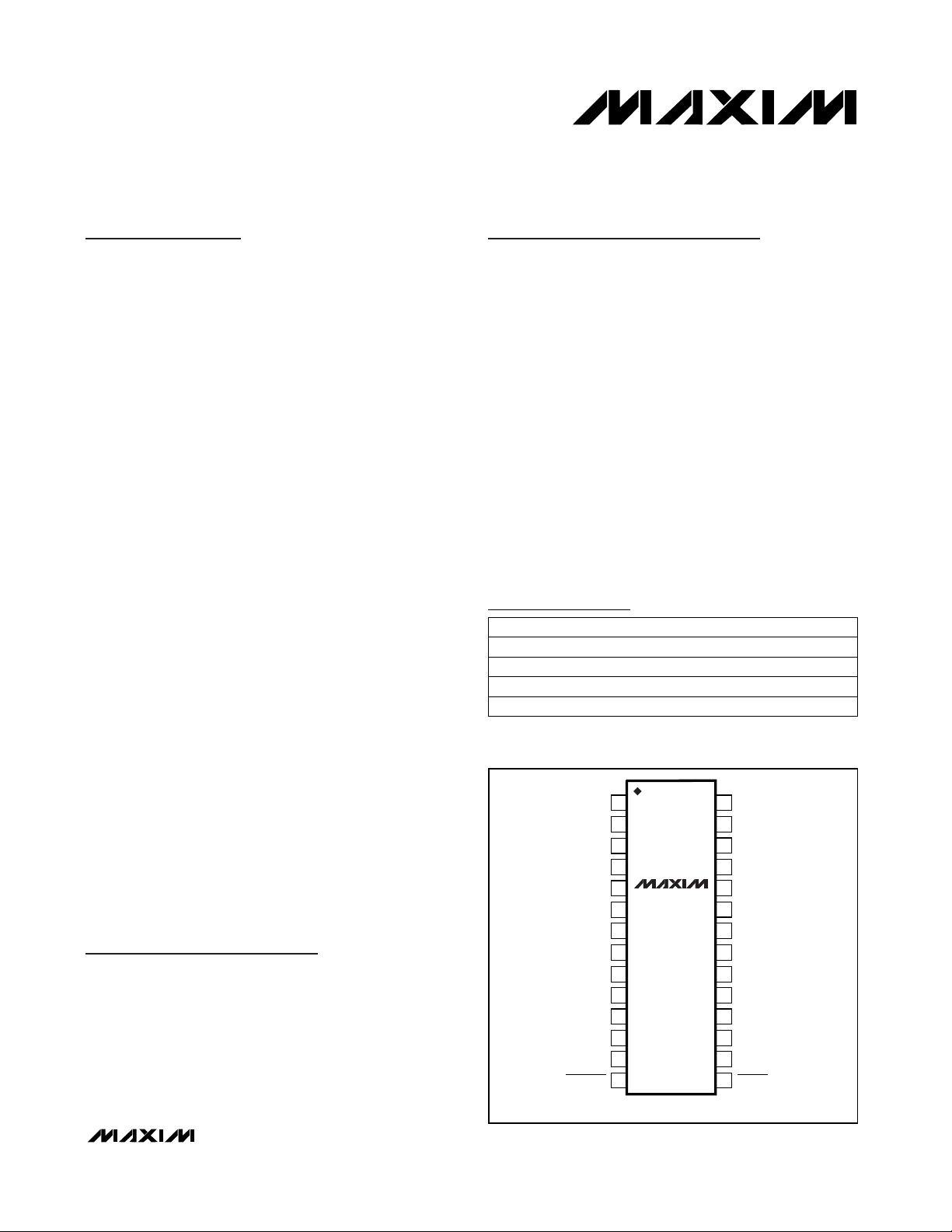
28
27
26
25
24
23
22
21
20
19
18
17
16
15
1
2
3
4
5
6
7
8
9
10
11
12
13
14
C1+
V+
V
CC
C1-
T1IN
T2IN
INVALID
T3IN
R1OUT
R2OUT
T4IN
R3OUT
T5IN
R1OUTB
FORCEOFF
FORCEON
T5OUT
R3IN
T4OUT
R2IN
R1IN
T3OUT
T2OUT
T1OUT
V-
C2-
GND
C2+
SSOP
TOP VIEW
MAX3238E
MAX3248E
___________________Pin Configuration
19-1632; Rev 1; 6/01
Ordering Information
AutoShutdown Plus is a trademark of Maxim Integrated Products.
TransZorb is a trademark of General Semiconductor Industries, Inc.
†
Covered by U.S. Patent numbers 4,636,930; 4,679,134;
4,777,577; 4,797,899; 4,809,152; 4,897,774; 4,999,761; and other
patents pending.
Cellular Data Cables
Modems
Battery-Powered Equipment
Peripherals
Data Cradles
Printers
Typical Operating Circuit appears at end of data sheet.
28 SSOP
28 SSOP
28 SSOP
28 SSOP
PIN-PACKAGETEMP. RANGE
0°C to +70°C
-40°C to +85°C
0°C to +70°C
-40°C to +85°CMAX3248EEAI
MAX3248ECAI
MAX3238EEAI
MAX3238ECAI
PART
For pricing, delivery, and ordering information, please contact Maxim/Dallas Direct! at
1-888-629-4642, or visit Maxim’s website at www.maxim-ic.com.
Stresses beyond those listed under “Absolute Maximum Ratings” may cause permanent damage to the device. These are stress ratings only, and functional
operation of the device at these or any other conditions beyond those indicated in the operational sections of the specifications is not implied. Exposure to
absolute maximum rating conditions for extended periods may affect device reliability.
MAX3238E/MAX3248E
+3.0V to +5.5V, 10nA, 250kbps RS-232 Transceivers
with ±15kV ESD-Protected I/O and Logic Pins
2 _______________________________________________________________________________________
ABSOLUTE MAXIMUM RATINGS
ELECTRICAL CHARACTERISTICS
(VCC= +3.0V to +5.5V, C1–C4 = 0.1µF (tested at 3.3V ±5%), C1–C4 = 0.22µF (tested at 3.3V ±10%), C1 = 0.047µF, and
C2–C4 = 0.33µF (tested at 5.0V ±10%), T
A
= T
MIN
to T
MAX
, unless otherwise noted. Typical values are at TA= +25°C.)
V
CC
...........................................................................-0.3V to +6V
V+ (Note 1) ...............................................................-0.3V to +7V
V- (Note 1) ................................................................+0.3V to -7V
V+ + |V-| (Note 1) .................................................................+13V
Input Voltages
T_IN, FORCEOFF, FORCEON ..............................-0.3V to +6V
R_IN .................................................................................±25V
Output Voltages
T_OUT...........................................................................±13.2V
R_OUT, INVALID ....................................-0.3V to (V
CC
+ 0.3V)
Short-Circuit Duration
T_OUT (one at a time) ............................................Continuous
Continuous Power Dissipation (T
A
= +70°C)
28-Pin SSOP (derate 9.52mW/°C above +70°C) .........762mW
Operating Temperature Ranges
MAX3238ECAI/MAX3248ECAI ...........................0°C to +70°C
MAX3238EEAI/MAX3248EEAI .........................-40°C to +85°C
Storage Temperature Range ............................-65°C to +150°C
Lead Temperature (soldering, 10s) ................................+300°C
Note 1: V+ and V- can have a maximum magnitude of +7V, but their absolute difference can not exceed +13V.
1.10 1.2
1.15 1.6
0.95 1.2
MAX3248E
FORCEON, FORCEOFF, and T_IN
wake-up threshold; V
CC
= 5.0V
FORCEON, FORCEOFF, and T_IN
wake-up threshold; V
CC
= 3.3V
T_IN (active)
FORCEON, FORCEOFF, and T_IN
wake-up threshold; V
CC
= 5.0V
FORCEON, FORCEOFF, and T_IN
wake-up threshold; V
CC
= 3.3V
T_IN (active)
FORCEON, FORCEOFF, and T_IN
wake-up threshold; V
CC
= 5.0V
FORCEON, FORCEOFF, and T_IN
wake-up threshold; V
CC
= 3.3V
T_IN (active)
FORCEON, FORCEOFF, and T_IN
wake-up threshold; V
CC
= 5.0V
FORCEON, FORCEOFF, and T_IN
wake-up threshold; V
CC
= 3.3V
T_IN (active)
PARAMETER MIN TYP MAX UNITS
Input Logic Threshold Low
0.8 1.20
V
Supply Current, AutoShutdown Plus
Disabled
0.5 2.0 mA
Supply Current, AutoShutdown Plus
Input Logic Threshold High
1.60 2.0
0.75 6 µA
V
10 300
2.10 2.4
1.30 2.0
MAX3238E
0.6 0.7
0.8 1.45
0.6 1.0
0.6 0.85
0.8 1.00
MAX3248E
Supply Current, Shutdown 10 300 nA
CONDITIONS
FORCEOFF = GND, R_IN = GND, T_IN = VCCor GND
MAX3238E
FORCEON = FORCEOFF = VCC, no load
Receivers idle, T_IN = VCCor GND, FORCEON =
GND, FORCEOFF = V
CC
R_IN = FORCEON = GND, FORCEOFF = V
CC,
T_IN = VCCor GND
nA
DC CHARACTERISTICS (VCC= +3.3V or +5.0V, TA= +25°C)
LOGIC INPUTS AND RECEIVER OUTPUTS
MAX3238E/MAX3248E
+3.0V to +5.5V, 10nA, 250kbps RS-232 Transceivers
with ±15kV ESD-Protected I/O and Logic Pins
_______________________________________________________________________________________ 3
ELECTRICAL CHARACTERISTICS (continued)
(VCC= +3.0V to +5.5V, C1–C4 = 0.1µF (tested at 3.3V ±5%), C1–C4 = 0.22µF (tested at 3.3V ±10%), C1 = 0.047µF, and
C2–C4 = 0.33µF (tested at 5.0V ±10%), T
A
= T
MIN
to T
MAX
, unless otherwise noted. Typical values are at TA= +25°C.)
Figure 4a
Figure 4a
Figure 4b
VCC= 5V, Figure 4b (Note 3)
VCC= 5V, Figure 4b
I
OUT
= 1.0mA
I
OUT
= -1.0mA
VCC= 5V, Figure 4b
V-0.3 0.3
Receiver Input Threshold to
INVALID Output Low
V
2.7
Receiver Input Threshold to
INVALID Output High
s15 30 60
Receiver or Transmitter Edge to
Shutdown (t
AUTOSHDN
)
µs25
Receiver or Transmitter Edge to
Transmitters Enabled (tWU)
µs60
Receiver Positive or Negative
Threshold to INVALID Low (t
INVL
)
V0.4
INVALID Output Voltage Low
V
V
CC -
0.6
INVALID Output Voltage High
µs0.3
Receiver Positive or Negative
Threshold to INVALID High (t
INVH
)
Positive threshold
Negative threshold -2.7
V-25 25
I
OUT
= -1.0mA
I
OUT
= 1.0mA
Input Voltage Range
VCC= 3.3V
Receivers disabled
T_IN, FORCEON, FORCEOFF (Note 2)
0.6 1.0
CONDITIONS
VCC= 5.0V
V
0.8 1.4
Input Threshold Low
VCC= 3.3V 1.5 2.4
VCC= 5.0V
V
2.0 2.4
Input Threshold High
V0.6Input Hysteresis
TA= +25°C kΩ357Input Resistance
V
V
CC
-V
CC
-
0.6 0.1
Output Voltage High
V0.4Output Voltage Low
µA±0.05 ±10Output Leakage Current
µA918Input Leakage Current
UNITSMIN TYP MAXPARAMETER
All transmitter outputs loaded with 3kΩ to ground V±5.0 ±5.4Output Voltage Swing
VCC= 0, T
OUT
= ±2V Ω300 50kOutput Resistance
VCC≤ 3.6V ±35 ±60
VCC> 3.6V
mA
±40 ±100
Output Short-Circuit Current
IEC 1000-4-2 Air-Gap Discharge Method ±15
IEC 1000-4-2 Contact Discharge Method ±8
Human Body Model
kV
±15
ESD Protection (R_IN, T_IN, R_OUT,
T_OUT, FORCEON, FORCEOFF,
INVALID, R_OUTB)
RECEIVER INPUTS
AutoShutdown (FORCEON = GND, FORCEOFF = VCC)
TRANSMITTER OUTPUTS
ESD PROTECTION
-6
-2
-4
2
0
4
6
-5
-3
1
-1
3
5
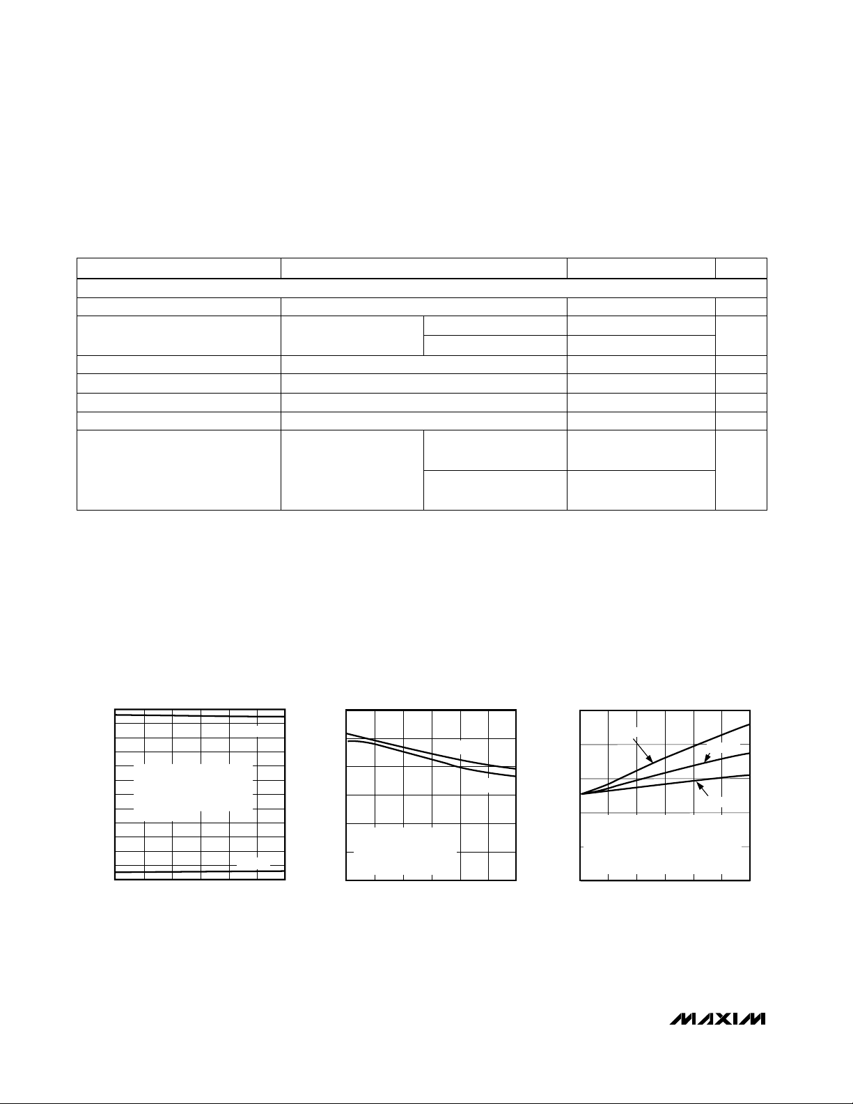
0 1000 1500500 2000 2500 3000
TRANSMITTER OUTPUT VOLTAGE
vs. LOAD CAPACITANCE
MAX3238E toc01
LOAD CAPACITANCE (pF)
TRANSMITTER OUTPUT VOLTAGE (V)
V
OUT-
V
OUT
+
FOR DATA RATES UP TO 250kbps
1 TRANSMITTER 250kbps
4 TRANSMITTERS 15.6kbps
ALL TRANSMITTERS LOADED
WITH 3kΩ + C
L
0
4
2
8
6
10
12
0 1000 1500500 2000 2500 3000
SLEW RATE vs. LOAD CAPACITANCE
MAX3238E toc02
LOAD CAPACITANCE (pF)
SLEW RATE (V/µs)
SR+
SR-
1 TRANSMITTER 250kbps
4 TRANSMITTERS 15.6kbps
ALL TRANSMITTERS LOADED
WITH 3kΩ + C
L
50
20
10
0
0 1000500 2000 3000
SUPPLY CURRENT vs. LOAD CAPACITANCE
WHEN TRANSMITTING DATA
30
MAX3238 TOC-03
SUPPLY CURRENT (mA)
LOAD CAPACITANCE (pF)
1500 2500
40
250kbps
20kbps
120kbps
1 TRANSMITTER 20kbps, 120 kbps, 250kbps
4 TRANSMITTERS 15.6kbps
ALL TRANSMITTERS LOADED
WITH 3kΩ + C
L
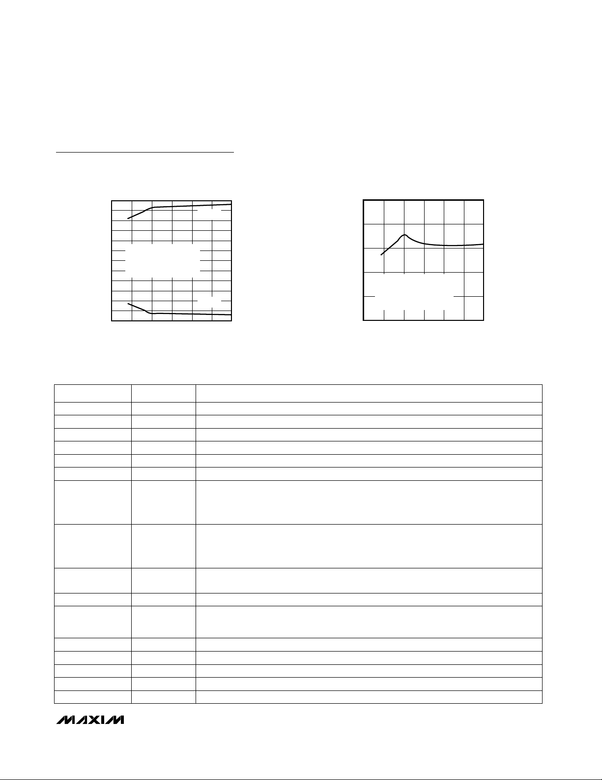
__________________________________________Typical Operating Characteristics
(VCC= +3.3V, 250kbps data rate, 0.1µF capacitors, all transmitters loaded with 3kΩ, TA= +25°C, unless otherwise noted.)
MAX3238E/MAX3248E
+3.0V to +5.5V, 10nA, 250kbps RS-232 Transceivers
with ±15kV ESD-Protected I/O and Logic Pins
4 _______________________________________________________________________________________
ELECTRICAL CHARACTERISTICS (continued)
(VCC= +3.0V to +5.5V, C1–C4 = 0.1µF (tested at 3.3V ±5%), C1–C4 = 0.22µF (tested at 3.3V ±10%), C1 = 0.047µF, and
C2–C4 = 0.33µF (tested at 5.0V ±10%), T
A
= T
MIN
to T
MAX
, unless otherwise noted. Typical values are at TA= +25°C.)
Note 2: The transmitter inputs have an active positive feedback resistor. The input current goes to zero when the inputs are at the
supply rails.
Note 3: During AutoShutdown only, a transmitter/receiver edge is defined as a transition through the transmitter/receiver input logic
wake-up thresholds.
CONDITIONS UNITSMIN TYP MAXPARAMETER
| t
PHL
- t
PLH
|
430
t
PHL
R_IN to R_OUT,
CL= 150pF
t
PLH
CL= 150pF to 1000pF
RL= 3kΩ, CL= 1000pF, one transmitter switching
CL= 150pF to 2500pF
0.15
VCC= 3.3V,
T
A
= +25°C,
RL= 3kΩ to 7kΩ,
measured from +3V to
-3V or -3V to +3V
Normal operation
Normal operation
| t
PHL
- t
PLH
|
µs
0.15
Receiver Propagation Delay
kbps250Maximum Data Rate
V/µs
630
Transition-Region Slew Rate
µs2.6Receiver Output Enable Time
µs2.4Receiver Output Disable Time
ns50
ns50Receiver Skew
Transmitter Skew
TIMING CHARACTERISTICS
MAX3238E/MAX3248E
+3.0V to +5.5V, 10nA, 250kbps RS-232 Transceivers
with ±15kV ESD-Protected I/O and Logic Pins
_______________________________________________________________________________________ 5
Typical Operating Characteristics (continued)
(VCC= +3.3V, 250kbps data rate, 0.1µF capacitors, all transmitters loaded with 3kΩ, TA= +25°C, unless otherwise noted.)
______________________________________________________________Pin Description
Output of the Valid Signal Detector. A logic 1 indicates if a valid RS-232 level is present on
receiver inputs.
INVALID
15
Noninverting Complementary Receiver Output. Always active.R1OUTB16
TTL/CMOS Transmitter Inputs (T5IN–T1IN). This pin has an active positive feedback resistor. Once driven to a valid logic level, the pin retains that level if left unconnected until
power is cycled.
T_IN17, 19, 22, 23, 24
TTL/CMOS Receiver Outputs (R3OUT–R1OUT)R_OUT18, 20, 21
Negative Terminal of Voltage-Doubler Charge-Pump CapacitorC1-25
RS-232 Transmitter Outputs (T1OUT–T5OUT)T_OUT5, 6, 7, 10, 12
RS-232 Receiver Inputs (R1IN–R3IN)R_IN8, 9, 11
Force-On Input. Drive high to override AutoShutdown Plus, keeping transmitters and
receivers on (FORCEOFF must be high) (Table 1). This pin has an active positive feedback
resistor. Once driven to a valid logic level, the pin retains that level if left unconnected until
power is cycled.
FORCEON13
Force-Off Input. Drive low to shut down transmitters, receivers (except R1OUTB), and onboard supply. This overrides AutoShutdown Plus and FORCEON (Table 1). This pin has an
active positive feedback resistor. Once driven to a valid logic level, the pin retains that
level if left unconnected until power is cycled.
FORCEOFF
14
-5.5V Generated by the Charge PumpV-4
Negative Terminal of Inverting Charge-Pump CapacitorC2-3
PIN
GroundGND2
Positive Terminal of Inverting Charge-Pump CapacitorC2+
1
FUNCTIONNAME
26 V
CC
+3.0V to +5.5V Supply Voltage
27 V+ +5.5V Generated by the Charge Pump
28 C1+ Positive Terminal of Voltage-Doubler Charge-Pump Capacitor
TRANSMITTER OUTPUT VOLTAGE
vs. SUPPLY VOLTAGE
6
5
4
3
2
1 TRANSMITTER 250kbps
1
4 TRANSMITTERS 15.6kbps
0
ALL TRANSMITTERS LOADED
-1
WITH 3kΩ +1000pF
-2
-3
-4
TRANSMITTER OUTPUT VOLTAGE (V)
-5
-6
2.0 3.0 3.52.5 4.0 4.5 5.0
SUPPLY VOLTAGE (V)
V
+
OUT
V
MAX3238E toc04
OUT-
50
40
30
20
SUPPLY CURRENT (mA)
10
0
2.0 3.0 3.52.5 4.0 4.5 5.0
SUPPLY CURRENT
vs. SUPPLY VOLTAGE
1 TRANSMITTER 250kbps
4 TRANSMITTERS 15.6kbps
ALL TRANSMITTERS LOADED
WITH 3kΩ +1000pF
SUPPLY VOLTAGE (V)
MAX3238E toc05

MAX3238E/MAX3248E
+3.0V to +5.5V, 10nA, 250kbps RS-232 Transceivers
with ±15kV ESD-Protected I/O and Logic Pins
6 _______________________________________________________________________________________
_______________Detailed Description
Dual Charge-Pump Voltage Converter
The MAX3238E/MAX3248Es’ internal power supply
consists of a regulated dual charge pump that provides
output voltages of +5.5V (doubling charge pump) and
-5.5V (inverting charge pump), regardless of the input
voltage (VCC) over the 3.0V to 5.5V range. The charge
pumps operate in a discontinuous mode: if the output
voltages are less than 5.5V, the charge pumps are
enabled; if the output voltages exceed 5.5V, the charge
pumps are disabled. Each charge pump requires a flying capacitor (C1, C2) and a reservoir capacitor (C3,
C4) to generate the V+ and V- supplies.
RS-232 Transmitters
The MAX3248E transmitters are inverting level translators
that convert a logic low of 0.6V and logic high of 1.2V to
5.0V EIA/TIA-232 levels. The MAX3238E transmitters are
inverting level translators that convert CMOS-logic levels
to 5.0V EIA/TIA-232 levels. The MAX3238E/MAX3248E
transmitters both guarantee a 250kbps data rate with
worst-case loads of 3kΩ in parallel with 1000pF, providing compatibility with PC-to-PC communication software
(such as LapLink™). Transmitters can be paralleled to
drive multiple receivers. Figure 1 shows a complete system connection.
LapLink is a trademark of Traveling Software.
When FORCEOFF is driven to ground, the transmitters
and receivers are disabled and the outputs go high
impedance, except for R1OUTB. When the AutoShutdown Plus circuitry senses that all receiver and
transmitter inputs are inactive for more than 30s, the
transmitters are disabled and the outputs go into a
high-impedance state, but the receivers remain active.
When the power is off, the MAX3238E/MAX3248E permit the outputs to be driven up to ±12V.
The transmitter inputs, FORCEON and FORCEOFF,
have a 400kΩ active positive-feedback resistor. Once
driven to a valid logic level, they will retain this level if
the driving signal is removed or goes high-impedance.
Unused transmitter inputs may be left unconnected.
RS-232 Receivers
The receivers convert RS-232 signals to CMOS-logic
output levels. All receivers have inverting three-state
outputs and are inactive in shutdown (FORCEOFF)
(Table 1). The MAX3238E/MAX3248E also feature an
extra, always-active noninverting output, R1OUTB. This
extra output monitors receiver activity while the other
receivers are high impedance, allowing Ring Indicator
to be monitored without forward biasing other devices
connected to the receiver outputs. This is ideal for systems where V
CC
is set to 0 in shutdown to accommo-
date peripherals, such as UARTs (Figure 2).
Table 1. Output Control Truth Table
FORCEON
FORCEOFF
AutoShutdown
Plus
OPERATION
STATUS
T_OUT R_OUT R1OUTB
X 0 X
Shutdown
(Forced Off)
High-Z High-Z Active
1 1 X
Normal Operation
(Forced On)
Active Active Active
0 1 <30s*
Normal
Operation
(AutoShutdown
Plus)
Active Active Active
0 1 >30s*
Shutdown
(AutoShutdown
Plus)
High-Z Active Active
X = Don’t care
*Time since last receiver or transmitter input transition.

MAX3238E/MAX3248E
+3.0V to +5.5V, 10nA, 250kbps RS-232 Transceivers
with ±15kV ESD-Protected I/O and Logic Pins
_______________________________________________________________________________________ 7
AutoShutdown Plus Mode
A 10nA supply current is achieved with Maxim’s
AutoShutdown Plus feature, which operates when
FORCEOFF is low and FORCEON is high. When the
MAX3238E/MAX3248E sense no valid signal transitions
on all receiver and transmitter inputs for 30s, the onboard power supply and drivers are shut off, reducing
supply current to 1µA. If the receiver inputs are in the
invalid range (-0.3V < R_IN < +0.3V) and the transmitter inputs are at GND or VCC, supply current is further
reduced to 10nA. This occurs if the RS-232 cable is
disconnected or if the connected peripheral transmitters are turned off. The system turns on again when a
valid transition is applied to any RS-232 receiver or
transmitter input. As a result, the system saves power
without changes to the existing BIOS or operating system. The INVALID output is high when the receivers are
active. Since INVALID indicates the receiver inputs’
condition, it can be used in any mode (Figure 3).
Figure 1. Interface Under Control of PMU
Figure 2. MAX3238E/MAX3248E detect RS-232 activity when
the UART and interface are shut down.
POWER
MANAGEMENT
UNIT OR
KEYBOARD
CONTROLLER
CPU
FORCEOFF
FORCEON
INVALID
I/O
CHIP
WITH
UART
MAX3238E/
MAX3248E
T1
T2
T3
T4
T5
R1
R2
R3
RS-232
V
CC
PROTECTION
DIODE
V
CC
SHDN = GND
I
V
CC
Rx
UART
Tx
GND
a) OLDER RS-232: POWERED-DOWN UART DRAWS CURRENT FROM ACTIVE
RECEIVER OUTPUT IN SHUTDOWN.
TO
LOGIC
µP
TRANSITION
DETECTOR
PREVIOUS
RS-232
5kΩ
I
PROTECTION
DIODE
V
CC
Rx
UART
Tx
GND
b) NEW MAX3238E/MAX3248E: IN SHUTDOWN, R1OUTB IS USED TO MONITOR
EXTERNAL DEVICES AND R1OUT IS THREE STATED, ELIMINATING A CURRENT
PATH THROUGH THE UART'S PROTECTION DIODE.
R1OUTB
R1OUT
THREE-STATED
T1IN
FORCEOFF = GND
MAX3238E
MAX3248E
R1IN
5kΩ
T1OUT

MAX3238E/MAX3248E
+3.0V to +5.5V, 10nA, 250kbps RS-232 Transceivers
with ±15kV ESD-Protected I/O and Logic Pins
8 _______________________________________________________________________________________
Tables 1 and 2 and Figure 3 summarize the MAX3238E/
MAX2348Es’ operating modes. FORCEON and FORCE-
OFF override the automatic circuitry and force the
transceiver into its normal operating state or into its lowpower standby state. When neither control is asserted,
the IC enters AutoShutdown Plus mode and selects
between these states automatically, based on the last
receiver or transmitter input edge received.
When shut down, the devices’ charge pumps turn off,
V+ decays to V
CC,
V- decays to ground, and the transmitter outputs are disabled (high impedance). The time
required to recover from shutdown is typically 25µs
(Figure 4b).
Software-Controlled Shutdown
If direct software control is desired, use INVALID to
indicate DTR or Ring Indicator signal. Tie FORCEOFF
and FORCEON together to bypass the AutoShutdown
Plus feature so the line acts like a SHDN input.
ESD Protection
As with all Maxim devices, ESD protection structures
are incorporated to protect against electrostatic discharges (ESDs) encountered during handling and
assembly. The MAX3238E/MAX3248E RS-232 transmitters and receivers, as well as the I/O have extra protection against static electricity found in normal operation.
Maxim’s engineers developed state-of-the-art structures to protect these pins against ESD of ±15kV without damage. After an ESD event, the MAX3238E/
MAX3248E keep working without latchup.
ESD protection can be tested in various ways. The pins
are characterized for protection to ±15kV and ±8kV
(see Electrical Characteristics).
ESD Test Conditions
Contact Maxim for a reliability report that documents
test setup, methodology, and results.
Human Body Model
Figure 5a shows the Human Body Model, and Figure
5b shows the current waveform it generates when discharged into a low impedance. This model consists of
a 100pF capacitor charged to the ESD voltage of inter-
Table 2. INVALID Truth Table
Figure 3a.
INVALID
Functional Diagram,
INVALID
Low
Figure 3b.
INVALID
Functional Diagram,
INVALID
High
Figure 3c. AutoShutdown Plus Logic
Figure 3d. Power-Down Logic
L
No
HYes
INVALID OUTPUT
RS-232 SIGNAL PRESENT AT
ANY RECEIVER INPUT
+0.3V
R_IN
-0.3V
INVALID ASSERTED IF ALL RECEIVER INPUTS ARE BETWEEN +0.3V AND -0.3V FOR
AT LEAST 60µs.
+2.7V
R_IN
-2.7V
INVALID DEASSERTED IF ANY RECEIVER INPUT HAS BEEN BETWEEN +2.7V AND -2.7V
FOR LESS THAN 60µs.
T_IN
R_IN
FORCEOFF
FORCEON
AUTOSHDN
EDGE
DETECT
EDGE
DETECT
FORCEON
60µs
TIMER
R
60µs
TIMER
R
FORCEOFF
S
30s TIMER
R
INVALID
INVALID
AUTOSHDN
POWERDOWN*
* POWER DOWN IS ONLY AN INTERNAL SIGNAL.
IT CONTROLS THE OPERATIONAL STATUS OF
THE TRANSMITTERS AND THE POWER SUPPLIES.

MAX3238E/MAX3248E
+3.0V to +5.5V, 10nA, 250kbps RS-232 Transceivers
with ±15kV ESD-Protected I/O and Logic Pins
_______________________________________________________________________________________ 9
est, which is then discharged into the test device
through a 1.5kΩ resistor.
IEC 1000-4-2
The IEC 1000-4-2 standard covers ESD testing and performance of finished equipment; it does not specifically
refer to integrated circuits. The MAX3238E/MAX3248E
help you design equipment that meets Level 4 (the highest level) of IEC 1000-4-2, without additional ESD protection components.
The major difference between tests done using the
Human Body Model and IEC 1000-4-2 is higher peak
current in IEC 1000-4-2. Because series resistance is
lower in the IEC 1000-4-2 ESD test model (Figure 6a),
the ESD withstand voltage measured to this standard is
generally lower than that measured using the Human
Body Model. Figure 6b shows the current waveform for
the ±8kV IEC 1000-4-2 Level 4 ESD Contact Discharge
test.
The Air-Gap test involves approaching the device with a
charged probe. The Contact Discharge method connects
the probe to the device before the probe is energized.
Machine Model
The Machine Model for ESD testing uses a 200pF storage capacitor and zero-discharge resistance. Its objective is to mimic the stress caused by contact that
occurs with handling and assembly during manufacturing. Of course, all pins (not just RS-232 inputs and outputs) require this protection during manufacturing.
Figure 4a. Receiver Positive/Negative Thresholds for
INVALID
Figure 4b. AutoShutdown Plus and
INVALID
Timing Diagram
INVALID HIGH
+2.7V
INDETERMINATE
+0.3V
0V
-0.3V
RECEIVER INPUT LEVELS
-2.7V
INVALID LOW
INDETERMINATE
INVALID HIGH
INVALID
REGION
RECEIVER
INPUTS
VOLTAGE
***
TRANSMITTER
INPUTS
VOLTAGE
TRANSMITTER
OUTPUTS
VOLTAGE
V
INVALID
OUTPUT
*ALL RECEIVERS/TRANSMITTERS INACTIVE
**ANY ONE RECEIVER/TRANSMITTER BECOMES ACTIVE FORCEON = GND, FORCEOFF = V
CC
0
I
NVL
V+
V
CC
0
V-
t
AUTOSHDN
t
t
WU
AUTOSHDN
t
WU
CC

MAX3238E/MAX3248E
10 ______________________________________________________________________________________
Therefore, the Machine Model is less relevant to the I/O
ports than the Human Body Model and IEC 1000-4-2.
Applications Information
Capacitor Selection
The capacitor type used for C1–C4 is not critical for
proper operation; polarized or nonpolarized capacitors
can be used. The charge pump requires 0.1µF capacitors for 3.3V operation. For other supply voltages, see
Table 3 for required capacitor values. Do not use values smaller than those listed in Table 3. Increasing the
capacitor values (e.g., by a factor of 2) reduces ripple
on the transmitter outputs and slightly reduces power
consumption. C2, C3, and C4 can be increased without
changing C1’s value. However, do not increase C1
without also increasing the values of C2, C3, C4,
and C
BYPASS
to maintain the proper ratios (C1 to the
other capacitors).
Power-Supply Decoupling
In most applications, decouple VCCto ground with a
0.1µF capacitor. Further increasing this capacitor value
reduces power-supply ripple and enhances noise margin. Connect the bypass capacitor as close to the IC as
possible.
Figure 5a. Human Body ESD Test Model
Figure 6a. IEC 1000-4-2 ESD Test Model
Figure 5b. Human Body Model Current Waveform
Figure 6b. IEC 1000-4-2 ESD Generator Current Waveform
+3.0V to +5.5V, 10nA, 250kbps RS-232 Transceivers
with ±15kV ESD-Protected I/O and Logic Pins
V
CC
(V)
C2, C3, C4
(µF)
3.0 to 3.6 0.22
C1, C
BYPASS
(µF)
0.22
4.5 to 5.5 0.33
3.0 to 5.5 1
0.047
0.22
Table 3. Required Minimum Capacitance
Values
3.15 to 3.6 0.10.1
1MΩ RD 1500Ω
R
C
PEAK-TO-PEAK RINGING
I
r
(NOT DRAWN TO SCALE)
HIGH-
VOLTAGE
DC
SOURCE
CHARGE-CURRENT
LIMIT RESISTOR
C
s
100pF
DISCHARGE
RESISTANCE
STORAGE
CAPACITOR
DEVICE
UNDER
TEST
AMPERES
IP 100%
90%
36.8%
10%
0
0
t
RL
TIME
t
DL
CURRENT WAVEFORM
50MΩ to 100MΩ RD 330Ω
R
C
CHARGE-CURRENT
LIMIT RESISTOR
HIGH-
VOLTAGE
DC
SOURCE
C
150pF
DISCHARGE
RESISTANCE
STORAGE
s
CAPACITOR
DEVICE
UNDER
TEST
I
100%
90%
PEAK
I
10%
tr = 0.7ns to 1ns
30ns
60ns
t

MAX3238E/MAX3248E
______________________________________________________________________________________ 11
Transmitter Outputs when
Recovering from Shutdown
Figure 7 shows two transmitter outputs when recovering
from shutdown mode. As they become active, the out-
puts are shown going to opposite RS-232 levels (one
transmitter input is high, the other is low). Each transmitter is loaded with 3kΩ in parallel with 2500pF. The
transmitter outputs display no ringing or undesirable
transients as they come out of shutdown. Note that the
transmitters are enabled only when the magnitude of Vexceeds approximately 3V.
High Data Rates
The MAX3238E/MAX3248E maintain the RS-232 ±5.0V
minimum transmitter output voltage even at high data
rates. Figure 8 shows a transmitter loopback test circuit. Figure 9 shows a loopback test result at 120kbps,
Figure 10. Loopback Test Result at 250kbps
Figure 9. Loopback Test Result at 120kbps
Figure 7. Transmitter Outputs when Recovering from Shutdown
or Powering Up
Figure 8. Loopback Test Circuit
+3.0V to +5.5V, 10nA, 250kbps RS-232 Transceivers
with ±15kV ESD-Protected I/O and Logic Pins
5V/div
FORCEON =
FORCEOFF
T2OUT
T1IN
+5V
0
+5V
2V/div
T1OUT
4µs/div
VCC = 3.3V, C1–C4 = 0.1µF, R
LOAD
= 3kΩ, C
LOAD
= 2500pF
V
CC
V
CC
MAX3238E
MAX3248E
V+
C3*
V-
C4
T_ OUT
C1
C2
C1+
C1-
C2+
C2-
T_ IN
T1OUT
R1OUT
2µs/div
VCC = 3.3V, C1–C4 = 0.1µF, C
LOAD
= 1000pF
T1IN
T1OUT
R1OUT
0
-5V
+5V
0
+5V
0
+5V
0
-5V
+5V
0
5kΩ
R_ IN
1000pF
R_ OUT
FORCEON
V
CC
*C3 CAN BE RETURNED TO VCC OR GND.
FORCEOFF
GND
2µs/div
VCC = 3.3V, C1–C4 = 0.1µF, C
LOAD
= 1000pF

MAX3238E/MAX3248E
Figure 11. Data Cable Application Example
12 ______________________________________________________________________________________
+3.0V to +5.5V, 10nA, 250kbps RS-232 Transceivers
with ±15kV ESD-Protected I/O and Logic Pins
28 1
C1+
+
C1
0.1µF
0.1µF
TVS
SUB-
MINIATURE
CONNECTOR
0.1µF
25
C1-
27
C3
C5
V+
±15kV ESD
26
24
23
22
19
17
PROTECTION
V
CC
T1IN T1OUT
T2IN T2OUT
T3IN T3OUT
T4IN T4OUT
T5IN
R1OUT21
R2OUT20
R3OUT18
MAX3238E
MAX3248E
±15kV ESD
PROTECTION
C2+
C2-
T5OUT
R2IN 9
R3IN 11
C2
3
0.1µF
4
V-
C4
0.1µF
5
6
7
10
12
8R1IN
DCD
DSR
RTS
CTS
DTR
1
6
RD
TD
RI
2
7
3
8
4
9
R1OUTB16
FORCEON
13
FORCEOFF
14
15
INVALID
CONTROL
GND
2
5

MAX3238E/MAX3248E
+3.0V to +5.5V, 10nA, 250kbps RS-232 Transceivers
with ±15kV ESD-Protected I/O and Logic Pins
______________________________________________________________________________________ 13
Typical Operating Circuit
___________________Chip Information
TRANSISTOR COUNT: 2110
and Figure 10 shows the same test at 250kbps. For
Figure 9, all transmitters were driven simultaneously at
120kbps into RS-232 loads in parallel with 1000pF. For
Figure 10, a single transmitter was driven at 250kbps,
and all transmitters were loaded with an RS-232 receiver in parallel with 1000pF.
Data Cable Applications
The MAX3238E/MAX3248Es’ ±15kV ESD protection on
both the RS-232 I/Os as well as the logic I/Os makes
them ideal candidates for data cable applications. A
data cable is both an electrical connection and a level
translator, allowing ultra-miniaturization of cell phones
and other small portable devices.
Previous data cable approaches suffered from complexity due to the required protection circuits on both
the logic side of the cable as well as on the RS-232
connections. The example shown in Figure 10 shows
the ease of using the MAX3238E/MAX3248E in data
cable applications.
The MAX3238E/MAX3248Es’ five-transmitter and threereceiver configuration is optimized for a data communication equipment (DCE) application, allowing full hardware handshaking. The 9-pin RS-232 connector is
configured for direct attachment to a PC’s serial port.
R1OUTB is also connected to the subminiature connector. This allows the remote system to shut down
until the PC asserts the ready to send (RTS) signal.
R1OUTB stays active when the MAX3238E/MAX3248E
is shut down (FORCEOFF = GND).
0.1µF
0.1µF
LOGIC
INPUTS
+3.3V
1µF
26
V
C1+
28
25
C1-
1
C2+ V-
3
C2-
24
T1IN T1OUT
23
T2IN T2OUT
22
T3IN T3OUT
19
T4IN T4OUT
T5IN
17
14
FORCEOFF
13
FORCEON
R1OUTB16
CC
MAX3238E
MAX3248E
T1
T2
T3
T4
T5
AutoShutdown Plus
INVALID
27
V+
4
5
6
7
10
12T5OUT
15
0.1µF*
0.1µF
RS-232
OUTPUTS
R1OUT 8R1IN21
LOGIC
OUTPUTS
R2OUT 9R2IN20
R3OUT 11
*C3 MAY BE RETURNED TO EITHER V
R1
5kΩ
R2
5kΩ
R3
GND
2
OR GND.
CC
R3IN18
5kΩ
RS-232
INPUTS

MAX3238E/MAX3248E
+3.0V to +5.5V, 10nA, 250kbps RS-232 Transceivers
with ±15kV ESD-Protected I/O and Logic Pins
________________________________________________________Package Information
Maxim cannot assume responsibility for use of any circuitry other than circuitry entirely embodied in a Maxim product. No circuit patent licenses are
implied. Maxim reserves the right to change the circuitry and specifications without notice at any time.
14 ____________________Maxim Integrated Products, 120 San Gabriel Drive, Sunnyvale, CA 94086 408-737-7600
© 2001 Maxim Integrated Products Printed USA is a registered trademark of Maxim Integrated Products.
SSOP.EPS
 Loading...