

Datasheet MAX3235EEWP, MAX3235ECPP, MAX3233EEWP, MAX3233EEPP, MAX3233ECWP Datasheet (Maxim)
...
For free samples & the latest literature: http://www.maxim-ic.com, or phone 1-800-998-8800.
For small orders, phone 1-800-835-8769.
________________General Description
The MAX3233E/MAX3235E are EIA/TIA-232 and V.28/V.24
communications interfaces with automatic shutdown/
wake-up features, high data-rate capabilities, and
enhanced electrostatic discharge (ESD) protection. All
transmitter outputs and receiver inputs are protected to
±15kV using IEC 1000-4-2 Air-Gap Discharge, to ±8kV
using IEC 1000-4-2 Contact Discharge, and to ±15kV
using the Human Body Model. The MAX3233E operates
from a +3.3V supply; the MAX3235E operates from +5.0V.
All devices achieve a 1µA supply current using Maxim’s
revolutionary AutoShutdown Plus™ feature. These
devices automatically enter a low-power shutdown
mode when the following two conditions occur: either
the RS-232 cable is disconnected or the transmitters of
the connected peripherals are inactive, and the UART
driving the transmitter inputs is inactive for more than
30 seconds. They turn on again when they sense a
valid transition at any transmitter or receiver input.
AutoShutdown Plus saves power without changes to
the existing BIOS or operating system.
The MAX3233E/MAX3235E have internal dual charge
pumps requiring no external capacitors. Both transceivers have a proprietary low-dropout transmitter output stage that enables true RS-232 performance from a
+3.0V to +3.6V supply for the MAX3233E or a +4.5V to
+5.5V supply for the MAX3235E. These devices are
guaranteed to operate up to 250kbps. Both are available in space-saving 20-pin wide SO or plastic DIP
packages.
________________________Applications
Subnotebook and Palmtop Computers
Cellular Phones
Battery-Powered Equipment
Hand-Held Equipment
Peripherals
Embedded Systems
____________________________Features
♦ ESD Protection for RS-232 I/O Pins
±15kV—Human Body Model
±8kV—IEC 1000-4-2, Contact Discharge
±15kV—IEC 1000-4-2, Air-Gap Discharge
♦ Latchup Free
♦ 1µA Supply Current
♦ AutoShutdown Plus—1997 EDN Magazine
Innovation of the Year
♦ Single-Supply Operation
+3.0V to +3.6V (MAX3233E)
+4.5V to +5.5V (MAX3235E)
♦ 250kbps Guaranteed Data Rate
♦ 6V/µs Guaranteed Slew Rate
♦ Meets EIA/TIA-232 Specifications Down to 3.0V
(MAX3233E)
♦ Internal Charge-Pump Capacitors
MAX3233E
†
/MAX3235E
†
±15kV ESD-Protected, 1µA, 250kbps, 3.3V/5V, Dual
RS-232 Transceivers with Internal Capacitors
________________________________________________________________
Maxim Integrated Products
1
19-1473; Rev 0; 4/99
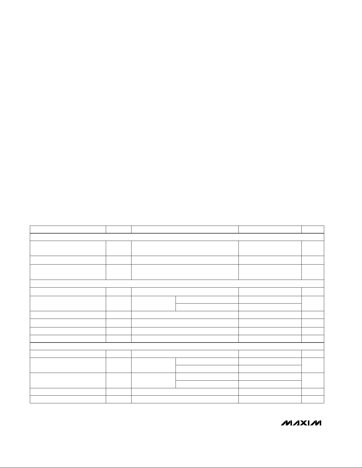
PART
MAX3233ECWP
0°C to +70°C
TEMP. RANGE PIN-PACKAGE
20 SO
AutoShutdown Plus is a trademark of Maxim Integrated Products.
_______________Ordering Information
Ordering Information continued at end of data sheet.
MAX3233E
MAX3235E
12
13
14
15
16
17
18
4
1
R2OUT R2IN
T2OUT
GND
V-
C2-
C2+
C1-
C1+
V+
V+
INVALID
T2IN
T1IN
FORCEON
R1OUT
T1OUT
R1IN
V
CC
FORCEOFF
2
9
10
5
6
7
8
3
19
20
11
CHARGE
PUMP
SO/DIP
Pin Configuration/
Functional Diagram
Typical Operating Circuit appears at end of data sheet.
MAX3233ECPP 0°C to +70°C 20 Plastic DIP
MAX3233EEPP -40°C to +85°C 20 Plastic DIP
MAX3233EEWP -40°C to +85°C 20 SO
†
Covered by U.S. Patent numbers 4,636,930; 4,679,134; 4,777,577;
4,797,899; 4,809,152; 4,897,774; 4,999,761; 5,649,210; and other
patents pending.
MAX3233E/MAX3235E
2 _______________________________________________________________________________________
ABSOLUTE MAXIMUM RATINGS
ELECTRICAL CHARACTERISTICS
(VCC= +3.0V to +3.6V for MAX3233E, VCC= +4.5V to +5.5V for MAX3235E; TA= T
MIN
to T
MAX
; unless otherwise noted. Typical val-
ues are at T
A
= +25°C.)
Stresses beyond those listed under “Absolute Maximum Ratings” may cause permanent damage to the device. These are stress ratings only, and functional
operation of the device at these or any other conditions beyond those indicated in the operational sections of the specifications is not implied. Exposure to
absolute maximum rating conditions for extended periods may affect device reliability.
VCCto GND (MAX3233E).........................................-0.3V to +4V
V
CC
to GND (MAX3235E).........................................-0.3V to +6V
V+ to GND (Note 1)..................................................-0.3V to +7V
V- to GND (Note 1)...................................................+0.3V to -7V
V+ +
|V-| (Note 1).................................................................+13V
Input Voltages
T_IN, FORCEON,
FORCEOFF to GND....................-0.3V to +6V
R_IN to GND...................................................................±25V
Output Voltages
T_OUT to GND.............................................................±13.2V
R_OUT, INVALID to GND......................-0.3V to (V
CC
+ 0.3V)
Short-Circuit Duration
T_OUT to GND......................................................Continuous
Continuous Power Dissipation (T
A
= +70°C)
Wide SO (derate 10mW/°C above +70°C)..................800mW
Plastic DIP (derate 11.11mW/°C above +70°C) .........889mW
Operating Temperature Ranges
MAX323_EC_P...................................................0°C to +70°C
MAX323_EE_P................................................-40°C to +85°C
Storage Temperature Range.............................-65°C to +150°C
Lead Temperature (soldering, 10sec).............................+300°C
Note 1: V+ and V- can have maximum magnitudes of 7V, but their absolute difference cannot exceed 13V.
FORCEON = GND, FORCEOFF = VCC,
all R_IN idle, all T_IN idle
TA= +25°C
CONDITIONS
kΩ357Input Resistance
V0.5Input Hysteresis
1.8 2.4
V
1.5 2.4
Input Threshold High
0.8 1.3
V
0.6 1.0
Input Threshold Low
V-25 +25Input Voltage Range
V
VCC- 0.6 VCC- 0.1
Output Voltage High
V0.4Output Voltage Low
µA110Supply Current, Shutdown
µA110
Supply Current,
AutoShutdown Plus
µA±0.01 ±1
Transmitter Input Hysteresis V0.5
V
2.4
Input Logic Threshold High
mA0.3 1
Supply Current,
AutoShutdown Plus Disabled
V0.8Input Logic Threshold Low
2
UNITSMIN TYP MAXSYMBOLPARAMETER
FORCEOFF = GND
TA= +25°C
T_IN, FORCEON, FORCEOFF
FORCEON = FORCEOFF = VCC, no load
T_IN, FORCEON, FORCEOFF
I
OUT
= -1.0mA
I
OUT
= 1.6mA
Input Leakage Current
DC CHARACTERISTICS (VCC= 3.3V for MAX3233E, VCC= 5.0V for MAX3235E, TA= +25°C.)
LOGIC INPUTS AND RECEIVER OUTPUTS
RECEIVER INPUTS
TA= +25°C
VCC= 5.0V, MAX3235E
VCC= 3.3V, MAX3233E
VCC= 5.0V, MAX3235E
VCC= 3.3V, MAX3233E
±15kV ESD-Protected, 1µA, 250kbps, 3.3V/5V, Dual
RS-232 Transceivers with Internal Capacitors
T_IN, FORCEON,
FORCEOFF
VCC= 5.0V, MAX3235E
VCC= 3.3V, MAX3233E
MAX3233E/MAX3235E
_______________________________________________________________________________________ 3
ELECTRICAL CHARACTERISTICS (continued)
(VCC= +3.0V to +3.6V for MAX3233E, VCC= +4.5V to +5.5V for MAX3235E; TA= T
MIN
to T
MAX
; unless otherwise noted. Typical val-
ues are at T
A
= +25°C.)
CONDITIONS
Ω300 10MOutput Resistance
V±5 ±5.4Output Voltage Swing
UNITSMIN TYP MAXSYMBOLPARAMETER
Figure 3a
sec15 30 60t
AUTOSHDN
Receiver or Transmitter Edge to
Transmitters Shut Down
µs100t
WU
Receiver or Transmitter Edge to
Transmitters Enabled
µs1t
INVH
Receiver Positive or Negative
Threshold to INVALID High
V
V
CC
- 0.6
INVALID, Output Voltage High
V0.4
INVALID Output Voltage Low
V-0.3 0.3
Receiver Input Threshold to
INVALID Output Low
-2.7
V
2.7
Receiver Input Threshold to
INVALID Output High
±15
±8R_IN, T_OUT kV
±15
µA
±25
Output Leakage Current
±60 mAOutput Short-Circuit Current
VCC= V+ = V- = 0, transmitter outputs = ±2V
All transmitter outputs loaded with 3kΩ to
ground
Figure 3b (Note 2)
Figure 3b (Note 2)
Figure 3b
I
OUT
= -1.0mA
I
OUT
= -1.6mA
Figure 3a
Human Body Model
V
OUT
= ± 12V
transmitters
disabled
IEC1000-4-2 Contact Discharge
IEC1000-4-2 Air Discharge
VCC= 0 or +4.5V to
5.5V (MAX3235E)
VCC= 0 or +3.0V to
3.6V (MAX3233E)
±15kV ESD-Protected, 1µA, 250kbps, 3.3V/5V, Dual
RS-232 Transceivers with Internal Capacitors
±25
MAX3233E
MAX3235E 50
µs
70
t
INVL
Receiver Positive or Negative
Threshold to INVALID Low
Figure 3b
TRANSMITTER OUTPUTS
ESD PROTECTION
AutoShutdown PLUS (FORCEON = GND, FORCEOFF = VCC)
Positive threshold
Negative threshold
ns
MAX3233E/MAX3235E
4 _______________________________________________________________________________________
TIMING CHARACTERISTICS (continued)
(VCC= +3.0V to +3.6V for MAX3233E, VCC= +4.5V to +5.5V for MAX3235E; TA= T
MIN
to T
MAX
; unless otherwise noted. Typical val-
ues are at T
A
= +25°C.)
Note 2: A transmitter/receiver edge is defined as a transition through the transmitter/receiver input logic thresholds.
Note 3: Transmitter skew is measured at the transmitter zero cross points.
CL= 150pF
to 2500pF
CL= 150pF
to 1000pF
R_IN to R_OUT,
CL= 150pF
RL= 3kΩ, CL= 1000pF,
one transmitter switching
VCC= 3.3V (MAX3233E),
VCC= 5.0V (MAX3235E),
TA= +25°C,
RL= 3kΩ to 7kΩ,
measured from +3V to -3V
or -3V to +3V
Normal operation
Normal operation
(Note 3)
CONDITIONS
100
ns
70
t
PHL
kbps250Maximum Data Rate
Receiver Propagation Delay
V/µs
430
630
Transition-Region Slew Rate
ns200Receiver Output Enable Time
ns200Receiver Output Disable Time
ns150
t
PHL
- t
PLH
Transmitter Skew
ns
180
t
PHL
- t
PLH
Receiver Skew
UNITSMIN TYP MAXSYMBOLPARAMETER
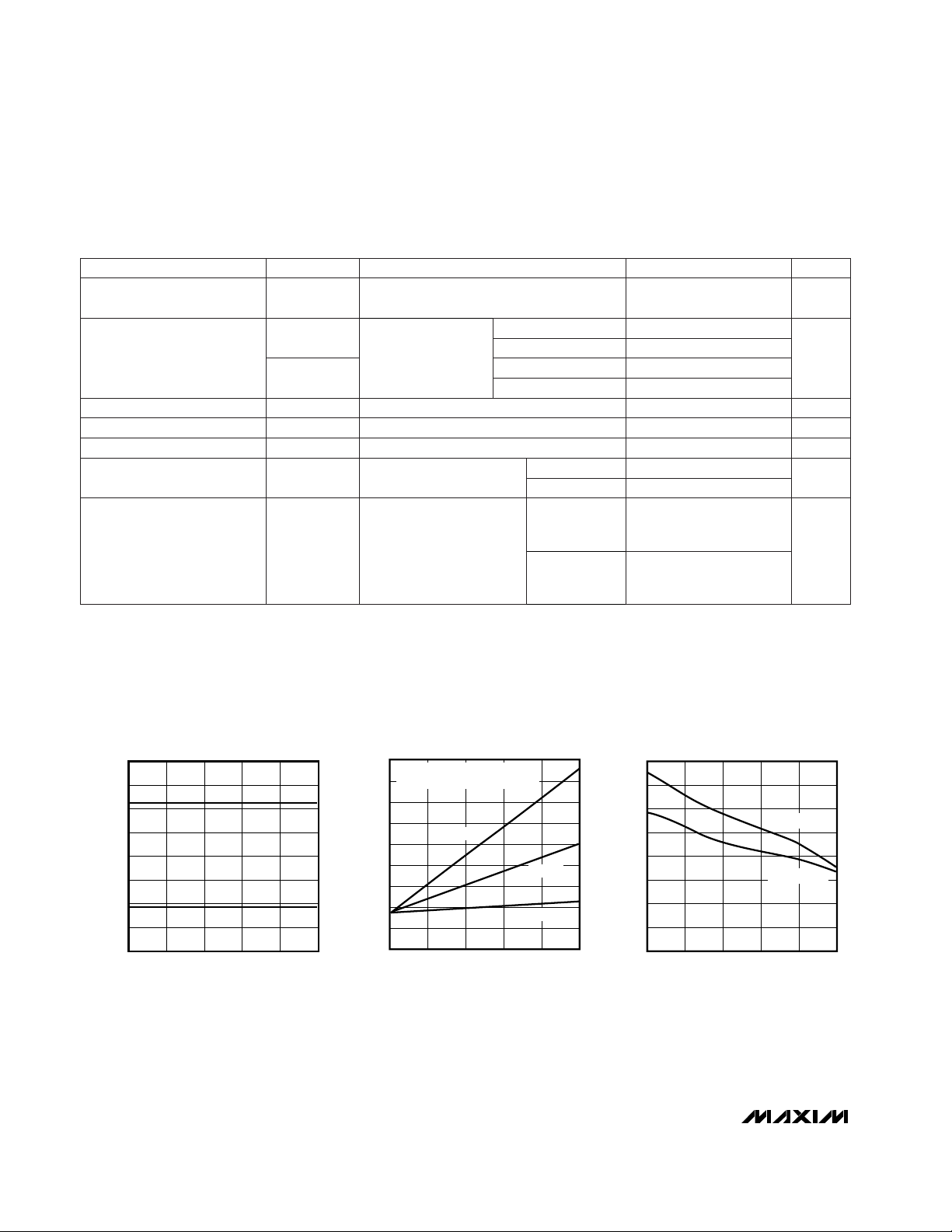
__________________________________________Typical Operating Characteristics
(VCC= +3.3V for MAX3233E, VCC= +5.0V for MAX3235E; 250kbps data rate; all transmitters loaded with 3kΩ and CL; TA= +25°C;
unless otherwise noted.)
±15kV ESD-Protected, 1µA, 250kbps, 3.3V/5V, Dual
RS-232 Transceivers with Internal Capacitors
150
250
t
PLH
MAX3233E
MAX3235E
MAX3233E
MAX3235E
50MAX3235E
MAX3233E
TRANSMITTER OUTPUT VOLTAGE vs.
LOAD CAPACITANCE
10.0
7.5
5.0
2.5
0
-2.5
-5.0
TRANSMITTER OUTPUT VOLTAGE (V)
-7.5
-10.0
0 1000 2000 3000 4000 5000
LOAD CAPACITANCE (pF)
+
V
OUT
-
V
OUT
MAX3233E/35Etoc01
SUPPLY CURRENT (mA)
OPERATING SUPPLY CURRENT
vs. LOAD CAPACITANCE
45
TRANSMITTER 1 AT DATA RATE
40
TRANSMITTER 2 AT 1/16 DATA RATE
35
30
25
20
15
10
5
0
0 20001000 3000 4000 5000
250kbps
120kbps
20kbps
LOAD CAPACITANCE (pF)
MAX3233E/35E toc02
SLEW RATE (V/µs)
SLEW RATE vs.
LOAD CAPACITANCE
16
14
12
10
8
6
4
2
0
0 1000 2000 3000 4000 5000
LOAD CAPACITANCE (pF)
SLEW RATE -
SLEW RATE +
MAX3233E/35Etoc01

MAX3233E/MAX3235E
_______________________________________________________________________________________
5
______________________________________________________________Pin Description
TTL/CMOS Receiver Outputs
FUNCTIONPIN NAME
1
3
7
8
9
10
11, 12
14
15
R2OUT
16
17
18
Invalid Signal Detector Output, active low. A logic high indicates that a valid RS-232
level is present on a receiver.
T2N
TTL/CMOS Transmitter Outputs
2
INVALID
5
T1OUT
RS-232 Transmitter Outputs
FORCEON
Force-On Input, active high. Drive high to override AutoShutdown Plus, keeping
transmitters and receivers active (FORCEOFF must be high) (Table 1).
13
R1IN
RS-232 Receiver Outputs
C1+
Positive terminal of the internal voltage-doubling charge-pump capacitor. Leave
unconnected or connect to an external 0.1µF capacitor. See
Charge Pump
Section.
V
CC
Supply Voltage (MAX3233E = +3.3V, MAX3235E = +5.0V)
FORCEOFF
Force-Off Input, active low. Drive low to shut down transmitters, receivers, and charge
pump. This overrides AutoShutdown Plus and FORCEON (Table 1).
V+ +5.5V generated by the charge pump. Do not connect.
C1-
Negative terminal of the internal voltage-doubling charge-pump capacitor. Leave
unconnected or connect to an external 0.1µF capacitor. See
Charge Pump
Section.
C2+ Positive terminal of the internal inverting charge-pump capacitor. Do not connect.
C2- Negative terminal of the internal inverting charge-pump capacitor. Do not connect.
V- -5.5V generated by the charge pump. Do not connect.
GND Ground
±15kV ESD-Protected, 1µA, 250kbps, 3.3V/5V, Dual
RS-232 Transceivers with Internal Capacitors
6 R1OUT
4 T1IN
19 T2OUT
20 R2IN

_______________Detailed Description
Dual Charge-Pump Voltage Converter
The MAX3233E/MAX3235E’s internal power supply
consists of a regulated dual charge pump that provides
output voltages of +5.5V (doubling charge pump) and
-5.5V (inverting charge pump), with no external capacitors. The charge pump operates in discontinuous
mode: if the output voltages are less than 5.5V, the
charge pump is enabled; if the output voltages exceed
5.5V, the charge pump is disabled.
RS-232 Transmitters
The transmitters are inverting level translators that
convert CMOS-logic levels to 5.0V EIA/TIA-232 levels.
The devices guarantee a 250kbps data rate with worstcase loads of 3kΩ in parallel with 1000pF, providing
compatibility with PC-to-PC communication software
(such as LapLink™). Transmitters can be paralleled to
drive multiple receivers. Figure 1 shows a complete
system connection.
When FORCEOFF is driven to ground or when the AutoShutdown Plus circuitry senses that all receiver and
transmitter inputs are inactive for more than 30sec, the
transmitters are disabled and the outputs go into a highimpedance state. When powered off or shut down, the
outputs can be driven to ±12V. The transmitter inputs
do not have pull-up resistors. Connect unused inputs to
GND or VCC.
RS-232 Receivers
The receivers convert RS-232 signals to CMOS-logic
output levels. They feature inverting outputs that always
remain active (Table 1).
The MAX3233E/MAX3235E feature an INVALID output
that is enabled low when no valid RS-232 voltage levels
have been detected on all receiver inputs. Because
INVALID indicates the receiver input’s condition, it is
independent of FORCEON and FORCEOFF states
(Figures 2 and 3).
AutoShutdown Plus Mode
The devices achieve a 1µA supply current with Maxim’s
AutoShutdown Plus feature, which operates when
FORCEOFF is high and a FORCEON is low. When these
devices do not sense a valid signal transition on any
receiver or transmitter input for 30sec, the on-board
charge pumps are shut down, reducing supply current
to 1µA. This occurs if the RS-232 cable is disconnected,
or if the connected peripheral transmitters are turned off
and the UART driving the transmitter inputs is inactive.
The system turns on again when a valid transition is
MAX3233E/MAX3235E
±15kV ESD-Protected, 1µA, 250kbps, 3.3V/5V, Dual
RS-232 Transceivers with Internal Capacitors
6 _______________________________________________________________________________________
MAX3233E
MAX3235E
I/O
CHIP
WITH
UART
CPU
RS-232
POWER-
MANAGEMENT
UNIT OR
KEYBOARD
CONTROLLER
FORCEOFF
FORCEON
INVALID
Figure 1. Interface Under Control of PMU
LapLink is a trademark of Traveling Software.
+0.3V
-0.3V
INVALID
R_IN
INVALID ASSERTED IF ALL RECEIVER INPUTS ARE BETWEEN +0.3V AND -0.3V FOR
AT LEAST 80µs.
80µs
TIMER
R
Figure 2a. INVALID Functional Diagram, INVALID Low
Figure 2b. INVALID Functional Diagram, INVALID High
+2.7V
R_IN
-2.7V
INVALID DEASSERTED IF ANY RECEIVER INPUT HAS BEEN ABOVE +2.7V OR BELOW
-2.7V FOR 1µs.
80µs
TIMER
R
INVALID

MAX3233E/MAX3235E
±15kV ESD-Protected, 1µA, 250kbps, 3.3V/5V, Dual
RS-232 Transceivers with Internal Capacitors
_______________________________________________________________________________________ 7
applied to any RS-232 receiver or transmitter input. As a
result, the system saves power without changes to the
existing BIOS or operating system.
Figures 2a and 2b depict invalid and valid RS-232
receiver voltage levels. INVALID indicates the receiver
input’s condition, and is independent of FORCEON and
FORCEOFF states. Figure 2 and Tables 1 and 2 summarize the operating modes. FORCEON and FORCE-
OFF override AutoShutdown Plus circuitry. When neither control is asserted, the IC selects between these
states automatically based on the last receiver or transmitter input edge received.
When shut down, the device’s charge pumps turn off,
V+ is pulled to V
CC
, V- is pulled to ground, and the
transmitter outputs are high impedance. The time
required to exit shutdown is typically 100µs (Figure 7).
Table 1. Output Control Truth Table
X = Don’t care
*
INVALID connected to FORCEON
**
INVALID connected to FORCEON and FORCEOFF
OPERATION STATUS FORCEON
FORCEOFF
VALID
RECEIVER
LEVEL
Rx or Tx EDGE
WITHIN 30sec
T_OUT R_OUT
Shutdown (Forced Off) X 0 X X High-Z Active
Normal Operation (Forced On) 1 1 X X Active Active
Normal Operation
(AutoShutdown Plus)
0 1 X Yes Active Active
Shutdown
(AutoShutdown Plus)
0 1 X No High-Z Active
Normal Operation
INVALID*
1 Yes X Active Active
Normal Operation
INVALID*
1 X Yes Active Active
Shutdown
INVALID*
1 No No High-Z Active
Normal Operation
(AutoShutdown)
INVALID* INVALID**
Yes X Active Active
Shutdown (AutoShutdown)
INVALID* INVALID**
No X High-Z Active
Figure 2c. AutoShutdown Plus Logic
POWERDOWN*
AUTOSHDN
FORCEOFF
FORCEON
POWERDOWN IS ONLY AN INTERNAL SIGNAL. IT CONTROLS THE OPERATIONAL
STATUS OF THE TRANSMITTERS AND THE POWER SUPPLIES.
*
Figure 2d. Power-Down Logic
EDGE
T_IN
DETECT
EDGE
R_IN
DETECT
FORCEON
*AUTOSHDN IS ONLY AN INTERNAL SIGNAL.
FORCEOFF
S
30sec
TIMER
R
AUTOSHDN*

By connecting FORCEON to INVALID, the device shuts
down when no valid receiver level and no receiver or
transmitter edge is detected for 30sec. It wakes up
when a valid receiver level or receiver or transmitter
edge is detected.
By connecting FORCEON and FORCEOFF to INVALID,
the device shuts down when no valid receiver level is
detected and wakes up when a valid receiver level is
detected.
A system with AutoShutdown Plus may need time to
wake up. Figure 4 shows a circuit that forces the
transmitters on for 100ms, allowing enough time
for another system to realize that the MAX3233E/
MAX3235E is awake. If another system outputs valid
RS-232 signal transitions within that time, the RS-232
ports on both systems remain enabled.
Software-Controlled Shutdown
If direct software control is desired, use INVALID to
indicate DTR or Ring Indicator signal. Tie FORCEOFF
and FORCEON together to bypass the AutoShutdown
Plus so the line acts like a SHDN input.
±15kV ESD Protection
As with all Maxim devices, ESD-protection structures are
incorporated on all pins to protect against electrostatic
discharges encountered during handling and assembly.
The driver outputs and receiver inputs have extra protection against static electricity. Maxim’s engineers have
developed state-of-the-art structures to protect these
pins against ESD of ±15kV without damage. The ESD
structures withstand high ESD in all states: normal
operation, shutdown, and powered down. After an ESD
MAX3233E /MAX3235E
±15kV ESD-Protected, 1µA, 250kbps, 3.3V/5V, Dual
RS-232 Transceivers with Internal Capacitors
8 _______________________________________________________________________________________
Table 2. INVALID Truth Table
LowNo
HighYes
INVALID OUTPUT
RS-232 SIGNAL
PRESENT AT ANY
RECEIVER INPUT
Figure 3a. Receiver Positive/Negative Thresholds for INVALID
V
CC
0
V+
V-
V
CC
0
INVALID
OUTPUT
TRANSMITTER
INPUTS
RECEIVER
INPUTS
}
INVALID
REGION
TRANSMITTER
OUTPUTS
t
AUTOSHDN
t
WU
t
WU
t
INVL
t
INVH
t
AUTOSHDN
Figure 3b. AutoShutdown Plus, INVALID, and READY Timing Diagram
INVALID HIGH
+2.7
INDETERMINATE
+0.3
0
-0.3
RECEIVER INPUT LEVELS (V)
-2.7
INVALID LOW
INDETERMINATE
INVALID HIGH

MAX3233E/MAX3235E
±15kV ESD-Protected, 1µA, 250kbps, 3.3V/5V, Dual
RS-232 Transceivers with Internal Capacitors
_______________________________________________________________________________________ 9
event, Maxim’s E versions keep working without
latchup, whereas competing RS-232 products can
latch and must be powered down to remove latchup.
ESD protection can be tested in various ways; the
transmitter outputs and receiver inputs of this product
family are characterized for protection to the following
limits:
1) ±15kV using the Human Body Model
2) ±8kV using the Contact Discharge method specified
in IEC 1000-4-2
3) ±15kV using IEC 1000-4-2’s Air-Gap Discharge
method
ESD Test Conditions
ESD performance depends on a variety of conditions.
Contact Maxim for a reliability report that documents
test setup, test methodology, and test results.
Human Body Model
Figure 5a shows the Human Body Model and Figure 5b
shows the current waveform it generates when discharged into a low impedance. This model consists of
a 100pF capacitor charged to the ESD voltage of interest, which is then discharged into the test device
through a 1.5kΩ resistor.
IEC 1000-4-2
The IEC 1000-4-2 standard covers ESD testing and performance of finished equipment; it does not specifically
refer to integrated circuits. The MAX3233E/MAX3235E
help you design equipment that meets Level 4 (the highest level) of IEC 1000-4-2, without the need for additional
ESD-protection components.
The major difference between tests done using the
Human Body Model and IEC 1000-4-2 is higher peak current in IEC 1000-4-2, because series resistance is lower
in the IEC 1000-4-2 model. Hence, the ESD withstand
voltage measured to IEC 1000-4-2 is generally lower than
FORCEON
MASTER SHDN LINE
0.1µF 1M
FORCEOFF
MAX3233E
MAX3235E
POWER-
MANAGEMENT
UNIT
Figure 4. AutoShutdown Plus Initial Turn-On to Wake Up
Another System
IP 100%
90%
36.8%
t
RL
TIME
t
DL
CURRENT WAVEFORM
PEAK-TO-PEAK RINGING
(NOT DRAWN TO SCALE)
I
r
10%
0
0
AMPERES
Figure 5b. Human Body Current Waveform
CHARGE-CURRENT
LIMIT RESISTOR
DISCHARGE
RESISTANCE
STORAGE
CAPACITOR
C
s
100pF
R
C
1M RD 1500Ω
HIGH-
VOLTAGE
DC
SOURCE
DEVICE
UNDER
TEST
Figure 5a. Human Body ESD Test Model
Figure 6a. IEC 1000-4-2 ESD Test Model
CHARGE CURRENT
LIMIT RESISTOR
DISCHARGE
RESISTANCE
STORAGE
CAPACITOR
C
s
150pF
R
C
50M to 100M RD 330Ω
HIGH-
VOLTAGE
DC
SOURCE
DEVICE
UNDER
TEST

that measured using the Human Body Model. Figure 6a
shows the IEC 1000-4-2 model, and Figure 6b shows the
current waveform for the ±8kV, IEC 1000-4-2, Level 4,
ESD contact-discharge test.
The air-gap test involves approaching the device with a
charged probe. The contact-discharge method connects
the probe to the device before the probe is energized.
Machine Model
The Machine Model for ESD tests all pins using a
200pF storage capacitor and zero discharge resistance. Its objective is to emulate the stress caused by
contact that occurs with handling and assembly during
manufacturing. Of course, all pins require this protection during manufacturing, not just RS-232 inputs and
outputs. Therefore, after PC board assembly, the
Machine Model is less relevant to I/O ports.
__________Applications Information
Charge Pumps
The MAX3233E/MAX3235E do not require external
capacitors to operate their internal charge pumps.
The MAX3235E can be operated down to 3.0V by paralleling the internal C1 capacitor with an external 0.1µF.
When using an external capacitor across the C1 terminals, check to confirm that the total supply voltage
measured from V+ to V- does not exceed the absolute
maximum voltage of 13V. With the external 0.1µF
capacitor added, the MAX3235E should not be used
with a supply greater than +3.9V.
Power-Supply Decoupling
In most applications, a 0.1µF VCCbypass capacitor is
adequate. Connect bypass capacitors as close to the
IC as possible.
Transmitter Outputs
when Exiting Shutdown
Figure 7 shows two transmitter outputs when exiting
shutdown mode. As they become active, the two transmitter outputs are shown going to opposite RS-232
levels (one transmitter input is high, the other is low).
MAX3233E/MAX3235E
±15kV ESD-Protected, 1µA, 250kbps, 3.3V/5V, Dual
RS-232 Transceivers with Internal Capacitors
10 ______________________________________________________________________________________
tr = 0.7ns to 1ns
30ns
60ns
t
100%
90%
10%
I
PEAK
I
Figure 6b. IEC 1000-4-2 ESD Generator Current Waveform
10µs/div
T1OUT
T2OUT
5V/div
0
2V/div
0
10V/div
0
VCC = 3.3V
FORCEON = FORCEOFF
Figure 7. Transmitter Outputs when Exiting Shutdown or
Powering Up
MAX3233E
MAX3235E
5k
R_ IN
R_ OUT
FORCEON
V
CC
C
BYPASS
V
CC
FORCEOFF
T_ OUT
T_ IN
GND
V
CC
1000pF
Figure 8. Loopback Test Circuit

MAX3233E/MAX3235E
±15kV ESD-Protected, 1µA, 250kbps, 3.3V/5V, Dual
RS-232 Transceivers with Internal Capacitors
______________________________________________________________________________________ 11
Each transmitter is loaded with 3kΩ in parallel with
1000pF. The transmitter outputs display no ringing or
undesirable transients as they come out of shutdown.
Note that the transmitters are enabled only when the
magnitude of V- exceeds approximately -3V.
High Data Rates
The MAX3233E/MAX3235E maintain the RS-232 ±5.0V
minimum transmitter output voltage even at high data
rates. Figure 8 shows a transmitter loopback test circuit. Figure 9 shows a loopback test result at 120kbps,
and Figure 10 shows the same test at 250kbps. For
Figure 9, all transmitters were driven simultaneously at
120kbps into RS-232 loads in parallel with 1000pF. For
Figure 10, a single transmitter was driven at 250kbps,
and all transmitters were loaded with an RS-232 receiver in parallel with 250pF.
Interconnection with 3V and 5V Logic
The MAX3233E/MAX3235E can directly interface with
various 5V logic families, including ACT and HCT
CMOS. See Table 3 for more information on possible
combinations of interconnections.
Figure 9. Loopback Test Result at 120kbps
2µs/div
T1IN
T1OUT
R1OUT
5V/div
5V/div
5V/div
VCC = 3.3V (MAX3233E), VCC = 5.0V (MAX3235E)
Figure 10. Loopback Test Result at 250kbps
2µs/div
T1IN
T1OUT
R1OUT
5V/div
5V/div
5V/div
VCC = 3.3V (MAX3233E), VCC = 5.0V (MAX3235E)
COMPATIBILITY
Compatible with all CMOS families
Compatible with ACT and HCT CMOS, and
with AC, HC, or CD4000 CMOS
Compatible with all TTL and CMOS families
DEVICE
V
CC
SUPPLY VOLTAGE
(V)
MAX3233E 3.3
MAX3233E 3.3
LOGIC POWER-SUPPLY
VOLTAGE
(V)
3.3
5
MAX3235E 53.3/5
Table 3. Logic Family Compatibility with Various Supply Voltages

MAX3233E/MAX3235E
Maxim cannot assume responsibility for use of any circuitry other than circuitry entirely embodied in a Maxim product. No circuit patent licenses are
implied. Maxim reserves the right to change the circuitry and specifications without notice at any time.
12
____________________Maxim Integrated Products, 120 San Gabriel Drive, Sunnyvale, CA 94086 408-737-7600
© 1999 Maxim Integrated Products Printed USA is a registered trademark of Maxim Integrated Products.
___________________Chip Information
TRANSISTOR COUNT: 1129
Typical Operating Circuit Ordering Information (continued)
C
BYPASS
MAX3233E
MAX3235E
R2OUT1
R1OUT6
FORCEON
INVALID
FORCEOFF
2
10
5
R2IN
20
GND
18
RS-232
OUTPUTS
TTL/CMOS
INPUTS
T2IN
3
T1IN
4
C2-
16
C2+
15
C1-
14
C1+
13
R1IN
8
T2OUT
19
T1OUT 7
V-
17
V+
11, 12
V
CC
V
CC
0.1µF
9
V
CC
RS-232
INPUTS
TTL/CMOS
OUTPUTS
5k
5k
AUTOSHUTDOWN
PLUS
PART TEMP. RANGE PIN-PACKAGE
MAX3235ECWP
MAX3235ECPP 0°C to +70°C
0°C to +70°C 20 SO
20 Plastic DIP
MAX3235EEWP -40°C to +85°C 20 SO
MAX3235EEPP -40°C to +85°C 20 Plastic DIP
±15kV ESD-Protected, 1µA, 250kbps, 3.3V/5V, Dual
RS-232 Transceivers with Internal Capacitors
 Loading...