

Page 1
General Description
The MAX3228E/AE and MAX3229E/AE are +2.5V to
+5.5V powered EIA/TIA-232 and V.28/V.24 communications interfaces with low power requirements, high datarate capabilities, and enhanced electrostatic discharge
(ESD) protection, in a chip-scale package (UCSP™)
and WLP Package. All transmitter outputs and receiver
inputs are protected to ±15kV using IEC 1000-4-2 AirGap Discharge, ±8kV using IEC 1000-4-2 Contact
Discharge, and ±15kV using the Human Body Model.
The MAX3228E/AE and MAX3229E/AE achieve a 1µA
supply current with Maxim’s AutoShutdown™ feature.
They save power without changes to existing BIOS or
operating systems by entering low-power shutdown
mode when the RS-232 cable is disconnected, or when
the transmitters of the connected peripherals are off.
The transceivers have a proprietary low-dropout transmitter output stage, delivering RS-232 compliant performance from a +3.1V to +5.5V supply, and RS-232
compatible performance with a supply voltage as low
as +2.5V. The dual charge pump requires only four
small 0.1µF capacitors for operation from a +3.0V supply. Each device is guaranteed to run at data rates of
250kbps while maintaining RS-232 output levels.
The MAX3228E/AE and MAX3229E/AE offer a separate
power-supply input for the logic interface, allowing configurable logic levels on the receiver outputs and transmitter inputs. Operating over a +1.65V to V
CC
range, V
L
provides the MAX3228E/AE and MAX3229E/AE compatibility with multiple logic families.
The MAX3229E/AE contains one receiver and one
transmitter. The MAX3228E/AE contains two receivers
and two transmitters. The MAX3228E/AE and
MAX3229E/AE are available in tiny chip-scale and WLP
packaging and are specified across the extended
industrial temperature range of -40°C to +85°C.
Applications
Personal Digital Assistants
Cell Phone Data Lump Cables
Set-Top Boxes
Handheld Devices
Cell Phones
Features
♦ 6 ✕ 5 Chip-Scale Package (UCSP) and WLP
Package
♦ ESD Protection for RS-232 I/O Pins:
±15kV—IEC 1000-4-2 Air-Gap Discharge
±8kV—IEC 1000-4-2 Contact Discharge
±15kV—Human Body Model
♦ 1µA Low-Power AutoShutdown
♦ 250kbps Guaranteed Data Rate
♦ Meets EIA/TIA-232 Specifications Down to +3.1V
♦ RS-232 Compatible to +2.5V Allows Operation
from Single Li+ Cell
♦ Small 0.1µF Capacitors
♦ Configurable Logic Levels
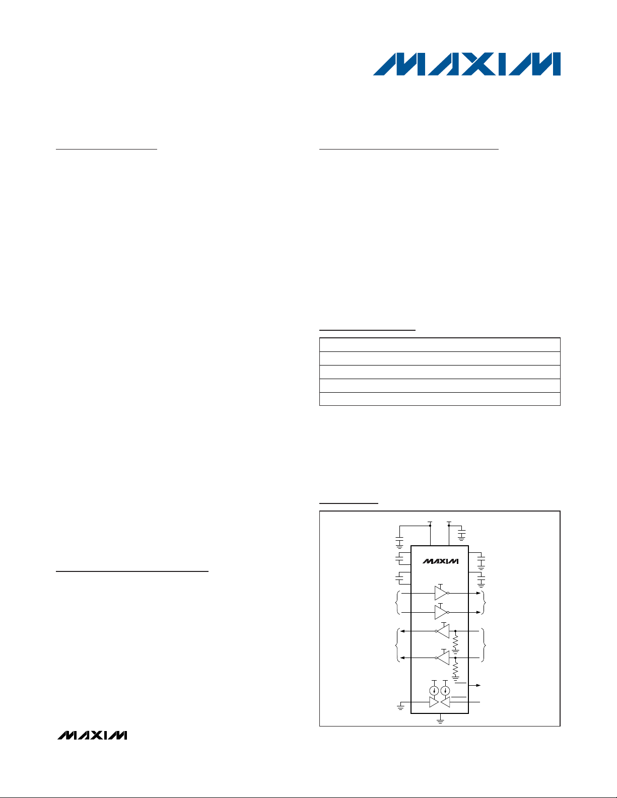
MAX3228E/MAX3228AE/MAX3229E/MAX3229AE
±15kV ESD-Protected +2.5V to +5.5V
RS-232 Transceivers in UCSP and WLP
________________________________________________________________
Maxim Integrated Products
1
V
L
MAX3228E/AE
5kΩ
T2OUT
T2IN
TTL/CMOS
INPUTS
C2-
C2+
C1-
C1+
A1 A5
C1
D1
A2
A3
A6
B6
B1
A4
E3
E4
E2
20μA20μA
E1
C5
B5
V-
V+
V
CC
2.5V TO 5.5V
C4
0.1μF
C3
0.1μF
C1
0.1μF
C
BYPASS
C2
0.1μF
0.1μF
FORCEOFFFORCEON
INVALID
T1OUT
T1IN
GND
V
L
TO POWERMANAGEMENT
UNIT
RS-232
OUTPUTS
V
L
V
L
V
L
1.65V TO 5.5V
V
L
5kΩ
R2IN
R2OUT
TTL/CMOS
OUTPUTS
D6
C6
E6
E5
R1IN
R1OUT
RS-232
INPUTS
V
L
V
L
0.1μF
Typical Operating Circuits
19-2139; Rev 2; 10/08
For pricing, delivery, and ordering information, please contact Maxim Direct at 1-888-629-4642,
or visit Maxim’s website at www.maxim-ic.com.
+
Denotes a lead-free/RoHS-compliant package.
*
Requires solder temperature profile described in the Absolute
Maximum Ratings section.
*
UCSP reliability is integrally linked to the user’s assembly methods, circuit board material, and environment. Refer to the UCSP
Reliabilitly Notice in the UCSP Reliability section of this data
sheet for more information.
T = Tape and reel.
Ordering Information
PART
BUMP-PACKAGE
MAX3228EEBV-T
6 x 5 UCSP*
MAX3228AEEWV+T
6 x 5 WLP
MAX3229EEBV-T
6 x 5 UCSP*
MAX3229AEEWV+T
6 x 5 WLP
UCSP is a trademark of Maxim Integrated Products, Inc.
AutoShutdown is a trademark of Maxim Integrated Products, Inc.
Typical Operating Circuits continued at end of data sheet.
Pin Configurations appear at end of data sheet.
TEMP RANGE
-40°C to +85°C
-40°C to +85°C
-40°C to +85°C
-40°C to +85°C
Page 2
MAX3228E/MAX3228AE/MAX3229E/MAX3229AE
±15kV ESD-Protected +2.5V to +5.5V
RS-232 Transceivers in UCSP and WLP
2 _______________________________________________________________________________________
ABSOLUTE MAXIMUM RATINGS
Stresses beyond those listed under “Absolute Maximum Ratings” may cause permanent damage to the device. These are stress ratings only, and functional
operation of the device at these or any other conditions beyond those indicated in the operational sections of the specifications is not implied. Exposure to
absolute maximum rating conditions for extended periods may affect device reliability.
VCCto GND...........................................................-0.3V to +6.0V
V+ to GND .............................................................-0.3V to +7.0V
V- to GND ..............................................................+0.3V to -7.0V
V+ to |V-| (Note 1) ................................................................+13V
V
L
to GND..............................................................-0.3V to +6.0V
Input Voltages
T_IN_, FORCEON, FORCEOFF to GND.....-0.3V to (V
L
+ 0.3V)
R_IN_ to GND ...................................................................±25V
Output Voltages
T
_OUT to GND ...............................................................±13.2V
R
_OUT INVALID to GND ............................-0.3V to (V
L
+ 0.3V)
INVALID to GND..........................................-0.3V to (V
CC
+0.3V)
Short-Circuit Duration T
_
OUT to GND........................Continuous
Continuous Power Dissipation (T
A
= +70°C)
6
✕ 5 UCSP (derate 10.1mW/°C above T
A
= +70°C)...805mW
6
✕ 5 WLP (derate 20mW/°C above T
A
= +70°C) ............1.6W
Operating Temperature Range ...........................-40°C to +85°C
Junction Temperature......................................................+150°C
Storage Temperature Range .............................-65°C to +150°C
Bump Temperature (Soldering) (Note 2)
Infrared (15s) ...............................................................+200°C
Vapor Phase (20s) .......................................................+215°C
ELECTRICAL CHARACTERISTICS
(VCC= +2.5V to +5.5V, VL= +1.65V to +5.5V, C1–C4 = 0.1µF, tested at +3.3V ±10%, TA= T
MIN
to T
MAX
. Typical values are at TA=
+25°C, unless otherwise noted.) (Note 3)
PARAMETER
CONDITIONS
UNITS
DC CHARACTERISTICS
VL Input Voltage Range V
L
V
FORCEON = GND
FORCEOFF = V
L
, all RIN open
10 µA
FORCEOFF = GND 10 µA
VCC Supply Current,
AutoShutdown
I
CC
FORCEON, FORCEOFF floating 1 mA
V
CC
Supply Current,
AutoShutdown Disabled
I
CC
FORCEON = FORCEOFF = V
L
no load
0.3 1 mA
FORCEON or FORCEOFF = GND,
V
CC
= VL =+5V
85
VL Supply Current I
L
FORCEON, FORCEOFF floating 1
µA
LOGIC INPUTS
Pullup Currents FORCEON, FORCEOFF to V
L
20 µA
Input Logic Low T_IN, FORCEON, FORCEOFF 0.4 V
Input Logic High T_IN, FORCEON, FORCEOFF 0.66 ✕ V
L
V
Transmitter Input Hysteresis 0.5 V
Input Leakage Current T_IN
±1 µA
RECEIVER OUTPUTS
Output Leakage Currents
R_OUT, receivers disabled, FORCEOFF =
GND or in AutoShutdown
µA
Output Voltage Low I
OUT
= 0.8mA 0.4 V
Output Voltage High I
OUT
= -0.5mA
V
Note 1: V+ and V- can have maximum magnitudes of 7V, but their absolute difference cannot exceed 13V.
Note 2: This device is constructed using a unique set of packaging techniques that impose a limit on the thermal profile the device
can be exposed to during board level solder attach and rework. This limit permits only the use of the solder profiles recommended in the industry-standard specification, JEDEC 020A, paragraph 7.6, Table 3 for IR/VPR and convection reflow. Preheating is required. Hand or wave soldering is not allowed.
SYMBOL
MIN TYP MAX
1.65 VCC + 0.3
±0.01
VL - 0.4 VL - 0.1
±10
Page 3
MAX3228E/MAX3228AE/MAX3229E/MAX3229AE
ELECTRICAL CHARACTERISTICS (continued)
(VCC= +2.5V to +5.5V, VL= +1.65V to +5.5V, C1–C4 = 0.1µF, tested at +3.3V ±10%, TA= T
MIN
to T
MAX
. Typical values are at TA=
+25°C, unless otherwise noted.) (Note 3)
PARAMETER
SYMBOL
CONDITIONS
MIN
TYP
MAX
UNITS
RECEIVER INPUTS
Input Voltage Range -25
V
VCC = +3.3V 0.6 1.2
Input Threshold Low TA = +25°C
V
CC
= +5.0V 0.8 1.7
V
VCC = +3.3V 1.3 2.4
Input Threshold High TA = +25°C
V
CC
= +5.0V 1.8 2.4
V
Input Hysteresis 0.5 V
Input Resistance 357kΩ
AUTO SHUTDOWN
Positive threshold 2.7
Receiver Input Threshold to
INVALID Output High
Figure 3a
V
Receiver Input Threshold to
INVALID Output Low
0.3 V
Receiver Positive or Negative
Threshold to INVALID High
t
INVH
VCC = +5.0V, Figure 3b 1 µs
Receiver Positive or Negative
Threshold to INVALID Low
t
INVL
VCC = +5.0V, Figure 3b 30 µs
Receiver Edge to Transmitters
Enabled
t
WU
VCC = +5.0V, Figure 3b
µs
INVALID OUTPUT
Output Voltage Low I
OUT
= 0.3mA 0.4 V
Output Voltage High I
OUT
= -0.5mA VCC - 0.4
V
TRANSMITTER OUTPUTS
VCC Mode Switch Point
(V
CC
Falling)
T_OUT = ±5.0V to ±3.7V
3.1 V
VCC Mode Switch Point
(V
CC
Rising)
T_OUT = ±3.7V to ±5.0V 3.3 3.7 V
V
C C
M od e S w i tch P oi nt H yster esi s
mV
VCC = +3.1V to
+5.5V, V
CC
falling
(T
A
= +25°C)
±5
Output Voltage Swing
All transmitter
outputs loaded with
3kΩ to ground.
V
CC
= +2.5V to
+3.1V, V
CC
rising
V
Output Resistance VCC = V+ = V- = 0, T_OUT = ±2V 300
Ω
Output Short-Circuit Current
mA
Output Leakage Current T_OUT = ±12V, transmitters disabled
µA
ESD PROTECTION
Human Body Model
IEC 1000-4-2 Air-Gap Discharge
R_IN, T_OUT
IEC 1000-4-2 Contact Discharge ±8
kV
±15kV ESD-Protected +2.5V to +5.5V
RS-232 Transceivers in UCSP and WLP
_______________________________________________________________________________________ 3
Negative threshold -2.7
-0.3
2.85
±3.7
100
VCC - 0.1
400
±5.4
10M
±15
±15
+25
±60
±25
Page 4
MAX3228E/MAX3228AE/MAX3229E/MAX3229AE
±15kV ESD-Protected +2.5V to +5.5V
RS-232 Transceivers in UCSP and WLP
4 _______________________________________________________________________________________
Note 3: VCCmust be greater than VL.
TIMING CHARACTERISTICS
(VCC= +2.5V to +5.5V, VL= +1.65V to +5.5V, C1–C4 = 0.1µF, tested at +3.3V ±10%, TA= T
MIN
to T
MAX
. Typical values are at TA=
+25°C, unless otherwise noted.) (Note 3)
PARAMETER
SYMBOL
CONDITIONS
MIN
TYP
MAX
UNITS
Maximum Data Rate
R
L
= 3kΩ, CL = 1000pF, one transmitter
switching
250 kbps
Receiver Propagation Delay
Receiver input to receiver output,
C
L
= 150pF
μs
Receiver Output Enable-Time VCC = VL = +5V
ns
Receiver Output Disable-Time VCC = VL = +5V
ns
Transmitter Skew
ns
Receiver Skew
50 ns
Transition Region Slew Rate
R
L
= 3kΩ to 7kΩ, CL = 150pF to
1000pF, T
A
= +25°C
630V/μs
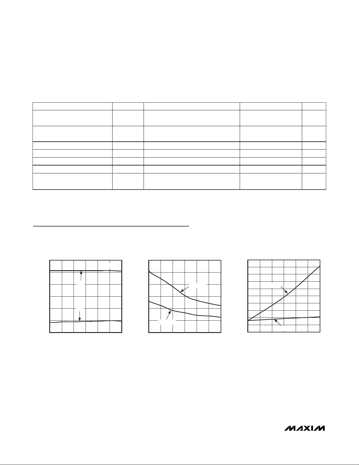
Typical Operating Characteristics
(VCC= +3.3V, 250kbps data rate, 0.1µF capacitors, all transmitters loaded with 3kΩ and CL, TA= +25°C, unless otherwise noted.)
0
6
4
2
8
10
12
14
16
18
20
0 1000500 1500 2000 2500 3000
OPERATING SUPPLY CURRENT
vs. LOAD CAPACITANCE (MAX3229E)
MAX3228E/28AE/29E/29AE toc03
LOAD CAPACITANCE (pF)
OPERATING SUPPLY CURRENT (mA)
250kbps
20kbps
| t
- t
PHL
| t
PHL
| 100
PLH
- t
|
PLH
0.15
200
200
TRANSMITTER OUTPUT VOLTAGE
vs. LOAD CAPACITANCE
6
4
V
2
0
-2
-4
TRANSMITTER OUTPUT VOLTAGE (V)
-6
0 1500 2000500 1000 2500 3000
OH
V
OL
LOAD CAPACITANCE (pF)
VCC RISING
30
25
20
MAX3228E/28AE/29E/29AE toc01
15
SLEW RATE (V/µs)
10
5
0
SLEW RATE vs. LOAD CAPACITANCE
VCC = 5.5V
VCC = 2.5V
0 2500 3000
1000500 1500 2000
LOAD CAPACITANCE (pF)
MAX3228E/28AE/29E/29AE toc02
Page 5
MAX3228E/MAX3228AE/MAX3229E/MAX3229AE
±15kV ESD-Protected +2.5V to +5.5V
RS-232 Transceivers in UCSP and WLP
_______________________________________________________________________________________ 5
PIN
MAX3228E/
MAX3228AE
NAME FUNCTION
A1 A1 V
CC
Supply Voltage. +2.5V to +5.5V supply voltage
A2 A2 C2+ Inverting Charge-Pump Capacitor Positive Terminal
A3 A3 C2- Inverting Charge-Pump Capacitor Negative Terminal
A4 A4 V- Negative Charge-Pump Output. -5.5V/-4.0V generated by charge pump.
A5 A5 V
L
Logic Voltage Input. Logic-level input for receiver outputs and transmitter inputs.
Connect V
L
to the system logic supply voltage or VCC if no logic supply is required.
A6, B6 A6 T_IN Transmitter Input(s)
B1 B1 V+
Positive Charge-Pump Output. +5.5V/+4.0V generated by charge pump. If charge
pump is generating +4.0V, the device has switched from RS-232 compliant to RS-232
compatible mode.
B2, B3, B4,
C2, C3, C4,
D2, D3, D4,
D5
D2, D3, D4,
D5
N.C.
No Connection. The MAX3228AE/MAX3229AE are not populated with solder bumps at
these locations. The MAX3228AE/MAX3229AE are populated with electrically isolated
bumps at these locations.
B5 B5
Active-High FORCEON Input. Drive FORCEON high to override automatic circuitry,
keeping transmitters and charge pumps on. Pulls itself high internally if not connected.
—
B6, D6,
E4, E6
N.C.
No Connection. These locations are populated with solder bumps, but are electrically
isolated.
C1 C1 C1+ Positive Regulated Charge-Pump Capacitor Positive Terminal
Pin Description
Typical Operating Characteristics (continued)
(VCC= +3.3V, 250kbps data rate, 0.1µF capacitors, all transmitters loaded with 3kΩ and CL, TA= +25°C, unless otherwise noted.)
0
6
4
2
8
10
12
14
16
18
20
2.5 3.53.0 4.0 4.5 5.0 5.5
OPERATING SUPPLY CURRENT
vs. SUPPLY VOLTAGE (MAX3229E)
MAX3228E/28AE/29E/29AE toc04
SUPPLY VOLTAGE (V)
OPERATING SUPPLY CURRENT (mA)
TRANSMITTER OUTPUT VOLTAGE vs.
SUPPLY VOLTAGE (V
10
8
6
4
2
0
-2
-4
TRANSMITTER OUTPUT VOLTAGE (V)
-6
-8
2.5 3.53.0 4.0 4.5 5.0 5.5
SUPPLY VOLTAGE (V)
CC
V
OH
V
OL
RISING)
MAX3228E/28AE/29E/29AE toc05
TRANSMITTER OUTPUT VOLTAGE vs.
SUPPLY VOLTAGE (V
10
8
6
4
2
0
-2
-4
TRANSMITTER OUTPUT VOLTAGE (V)
-6
-8
2.5 3.53.0 4.0 4.5 5.0 5.5
SUPPLY VOLTAGE (V)
FALLING)
CC
V
OH
V
OL
MAX3229E/
MAX3229AE
MAX3228E/28AE/29E/29AE toc06
B2, B3, B4,
C2, C3, C4,
FORCEON
Page 6

MAX3228E/MAX3228AE/MAX3229E/MAX3229AE
±15kV ESD-Protected +2.5V to +5.5V
RS-232 Transceivers in UCSP and WLP
6 _______________________________________________________________________________________
Detailed Description
Dual-Mode Regulated Charge-Pump
Voltage Converter
The MAX3228E/AE and MAX3229E/AE internal power
supply consists of a dual-mode regulated charge
pump. For supply voltages above +3.7V, the charge
pump will generate +5.5V at V+ and -5.5V at V-. The
charge pumps operate in a discontinuous mode. If the
output voltages are less than ±5.5V, the charge pumps
are enabled, if the output voltages exceed ±5.5V, the
charge pumps are disabled.
For supply voltages below +2.85V, the charge pump
will generate +4.0V at V+ and -4.0V at V-. The charge
pumps operate in a discontinuous mode. If the output
voltages are less than ±4.0V, the charge pumps are
enabled, if the output voltages exceed ±4.0V, the
charge pumps are disabled.
Each charge pump requires a flying capacitor (C1, C2)
and a reservoir capacitor (C3, C4) to generate the V+
and V- supply voltages.
Voltage Generation in the
Switchover Region
The MAX3228E/AE and MAX3229E/AE include a
switchover circuit between these two modes that have
approximately 400mV of hysteresis around the
switchover point. The hysteresis is shown in Figure 1.
This large hysteresis eliminates mode changes due to
power-supply bounce.
For example, a three-cell NiMh battery system starts at
VCC= +3.6V, and the charge pump will generate an
output voltage of ±5.5V. As the battery discharges, the
PIN
MAX3228E/
MAX3228AE
NAME FUNCTION
C5 C5
Active-Low FORCEOFF Input. Drive FORCEOFF low to shut down transmitters,
receivers, and on-board charge pump. This overrides all automatic circuitry and
FORCEON. Pulls itself high internally if not connected.
C6, D6 C6 R_OUT Receiver Output(s)
D1 D1 C1- Positive Regulated Charge-Pump Capacitor Negative Terminal
E1 E1 GND Ground
E2 E2 INVALID
Valid Signal Detector Output. INVALID is enabled low if no valid RS-232 level is present
on any receiver input.
E3, E4 E3 T_OUT RS-232 Transmitter Output(s)
E5, E6 E5 R_IN RS-232 Receiver Input(s)
Pin Description (continued)
SYSTEM SUPPLY (V) VCC (V) VL (V) RS-232 MODE
1 Li+ Cell +2.4 to +4.2 Regulated System Voltage Compliant/Compatible
3 NiCad/NiMh Cells +2.4 to +3.8 Regulated System Voltage Compliant/Compatible
Regulated Voltage Only
(V
CC
falling)
+3.0 to +5.5 +3.0 to +5.5 Compliant
Regulated Voltage Only
(V
CC
falling)
+2.5 to +3.0 +2.5 to +3.0 Compatible
Table 1. Operating Supply Options
Figure 1. V+ Switchover for Changing V
CC
0
6V
4V
0
20ms/div
V
CC
V+
MAX3229E/
MAX3229AE
FORCEOFF
Page 7

MAX3228E/MAX3228AE/MAX3229E/MAX3229AE
MAX3228E/AE and MAX3229E/AE maintain the outputs
in regulation until the battery voltage drops below +3.1V.
Then the output regulation points change to ±4.0V
When VCCis rising, the charge pump will generate an
output voltage of ±4.0V, while VCCis between +2.5V
and +3.5V. When VCCrises above the switchover voltage of +3.5V, the charge pump switches modes to
generate an output of ±5.5V.
Table 1 shows different supply schemes and their operating voltage ranges.
RS-232 Transmitters
The transmitters are inverting level translators that convert CMOS-logic levels to RS-232 levels. The
MAX3228E/AE and MAX3229E/AE will automatically
reduce the RS-232 compliant levels (±5.5V) to RS-232
compatible levels (±4.0V) when VCCfalls below
approximately +3.1V. The reduced levels also reduce
supply current requirements, extending battery life.
Built-in hysteresis of approximately 400mV for V
CC
ensures that the RS-232 output levels do not change if
VCCis noisy or has a sudden current draw causing the
supply voltage to drop slightly. The outputs will return to
RS-232 compliant levels (±5.5V) when VCCrises above
approximately +3.5V.
The MAX3228E/AE and MAX3229E/AE transmitters
guarantee a 250kbps data rate with worst-case loads of
3kΩ in parallel with 1000pF.
When FORCEOFF is driven to ground, the transmitters
and receivers are disabled and the outputs become
high impedance. When the AutoShutdown circuitry
senses that all receiver and transmitter inputs are inactive for more than 30µs, the transmitters are disabled
and the outputs go to a high-impedance state. When
the power is off, the MAX3228E/AE and MAX3229E/AE
permit the transmitter outputs to be driven up to ±12V.
The transmitter inputs do not have pullup resistors.
Connect unused inputs to GND or V
L
.
RS-232 Receivers
The MAX3228E/AE and MAX3229E/AE receivers convert RS-232 signals to logic output levels. All receivers
have inverting three-state outputs and can be active or
inactive. In shutdown (FORCEOFF = low) or in
AutoShutdown, the MAX3228E/AE and MAX3229E/AE
receivers are in a high-impedance state (Table 3).
The MAX3228E/AE and MAX3229E/AE feature an
INVALID output that is enabled low when no valid
RS-232 signal levels have been detected on any
receiver inputs. INVALID is functional in any mode
(Figures 2 and 3).
Figure 2c. MAX322_E AutoShutdown Logic
FORCEOFF
POWER DOWN
INVALID
FORCEON
INVALID IS AN INTERNALLY GENERATED SIGNAL
THAT IS USED BY THE AUTOSHUTDOWN LOGIC
AND APPEARS AS AN OUTPUT OF THE DEVICE.
POWER DOWN IS ONLY AN INTERNAL SIGNAL.
IT CONTROLS THE OPERATIONAL STATUS OF
THE TRANSMITTERS AND THE POWER SUPPLIES.
V
L
V
L
V
CC
Figure 2a. MAX322_E Entering 1µA Supply Mode via
AutoShutdown
+0.3V
-0.3V
INVALID
TO MAX322 _E
POWER SUPPLY
AND TRANSMITTERS
R_IN
*TRANSMITTERS ARE DISABLED, REDUCING SUPPLY CURRENT TO 1μA IF
ALL RECEIVER INPUTS ARE BETWEEN +0.3V AND -0.3V FOR AT LEAST 30μs.
30μs
COUNTER
R
Figure 2b. MAX322_E with Transmitters Enabled Using
AutoShutdown
+2.7V
-2.7V
INVALID
TO MAX322 _E
POWER SUPPLY
R_IN
*TRANSMITTERS ARE ENABLED IF:
ANY RECEIVER INPUT IS GREATER THAN +2.7V OR LESS THAN -2.7V.
ANY RECEIVER INPUT HAS BEEN BETWEEN +0.3V AND -0.3V FOR LESS THAN 30μs.
30μs
COUNTER
R
±15kV ESD-Protected +2.5V to +5.5V
RS-232 Transceivers in UCSP and WLP
_______________________________________________________________________________________ 7
Page 8

AutoShutdown
The MAX3228E/AE and MAX3229E/AE achieve a 1µA
supply current with Maxim’s AutoShutdown feature,
which operates when FORCEON is low and FORCEOFF
is high. When these devices sense no valid signal levels on all receiver inputs for 30µs, the on-board charge
pump and drivers are shut off, reducing VCCsupply
current to 1µA. This occurs if the RS-232 cable is disconnected or the connected peripheral transmitters are
turned off. The device turns on again when a valid level
is applied to any RS-232 receiver input. As a result, the
system saves power without changes to the existing
BIOS or operating system.
Table 3 and Figure 2c summarize the MAX3228E/AE
and MAX3229E/AE operating modes. FORCEON and
FORCEOFF override AutoShutdown. When neither control is asserted, the IC selects between these states
automatically, based on receiver input levels. Figures
2a, 2b, and 3a depict valid and invalid RS-232 receiver
levels. Figures 3a and 3b show the input levels and timing diagram for AutoShutdown operation.
A system with AutoShutdown may need time to wake
up. Figure 4 shows a circuit that forces the transmitters
on for 100ms, allowing enough time for the other
system to realize that the MAX3228E/AE and
MAX3229E/AE are active. If the other system transmits
valid RS-232 signals within that time, the RS-232 ports
on both systems remain enabled.
When shut down, the device’s charge pumps are off,
V+ is pulled to V
CC
, V- is pulled to ground, and the
transmitter outputs are high-impedance. The time
required to exit shutdown is typically 100µs (Figure 3b).
FORCEON and
FORCEOFF
In case FORCEON and FORCEOFF are inaccessible,
these pins have 60kΩ (typ) pullup resistors connected to
VL(Table 2). Therefore, if FORCEON and FORCEOFF are
not connected, the MAX3228E/AE and MAX3229E/AE
will always be active. Pulling these pins to ground will
draw current from the VLsupply. This current can be calculated from the voltage supplied at VLand the 60kΩ
(typ) pullup resistor.
VLLogic Supply Input
Unlike other RS-232 interface devices, where the
receiver outputs swing between 0 and VCC, the
MAX3228E/MAX3228AE/MAX3229E/MAX3229AE
±15kV ESD-Protected +2.5V to +5.5V
RS-232 Transceivers in UCSP and WLP
8 _______________________________________________________________________________________
Figure 3. AutoShutdown Trip Levels
V-
V
CC
0
V+
0
V
CC
t
INVL
t
WU
INVALID
REGION
RECEIVER
INPUT
VOLTAGE
(V)
INVALID
OUTPUT
(V)
t
INVH
TRANSMITTERS ENABLED, INVALID HIGH
RECEIVER INPUT LEVELS
AUTOSHUTDOWN, TRANSMITTERS DISABLED,
1μA SUPPLY CURRENT, INVALID LOW
TRANSMITTERS ENABLED, INVALID HIGH
a)
b)
-2.7V
-0.3V
+2.7V
+0.3V
0
INDETERMINATE
INDETERMINATE
Figure 4. AutoShutdown with Initial Turn-On to Wake Up a
Mouse or Another System
FORCEON
MASTER SHDN LINE
0.1μF1MΩ
FORCEOFF
MAX3228E/AE
MAX3229E/AE
POWER-
MANAGEMENT
UNIT
PIN NAME
MECHANISM
FORCEON High Internal pullup
FORCEOFF High Internal pullup
Table 2. Power-On Default States
POWER-ON DEFAULT
Page 9

MAX3228E/MAX3228AE/MAX3229E/MAX3229AE
MAX3228E/AE and MAX3229E/AE feature a separate
logic supply input (V
L
) that sets VOHfor the receiver
and INVALID outputs. The transmitter inputs (T_IN),
FORCEON and FORCEOFF, are also referred to VL.
This feature allows maximum flexibility in interfacing to
different systems and logic levels. Connect VLto the
system’s logic supply voltage (+1.65V to +5.5V), and
bypass it with a 0.1µF capacitor to GND. If the logic
supply is the same as VCC, connect VLto VCC. Always
enable VCCbefore enabling the VLsupply. VCCmust
be greater than or equal to the VLsupply.
Software-Controlled Shutdown
If direct software control is desired, connect FORCEOFF and FORCEON together to disable AutoShutdown.
The microcontroller then drives FORCEOFF and
FORCEON like a SHDN input, INVALID can be used to
alert the microcontroller to indicate serial data activity.
±15kV ESD Protection
As with all Maxim devices, ESD-protection structures are
incorporated on all pins to protect against electrostatic
discharges encountered during handling and assembly.
The driver outputs and receiver inputs of the
MAX3228E/AE and MAX3229E/AE have extra protection
against static electricity. Maxim’s engineers have developed state-of-the-art structures to protect these pins
against ESD of ±15kV without damage. The ESD structures withstand high ESD in all states: normal operation,
shutdown, and powered down. After an ESD event
Maxim’s E versions keep working without latchup,
whereas competing RS-232 products can latch and
must be powered down to remove latchup.
ESD protection can be tested in various ways; the transmitter outputs and receiver inputs of this product family
are characterized for protection to the following limits:
1) ±15kV using the Human Body Model.
2) ±8kV using the Contact Discharge method specified
in IEC 1000-4-2.
3) ±15kV using the IEC 1000-4-2 Air-Gap method.
ESD Test Conditions
ESD performance depends on a variety of conditions.
Contact Maxim for a reliability report that documents test
setup, test methodology, and test results.
Human Body Model
Figure 5a shows the Human Body Model, and Figure 5b
shows the current waveform it generates when discharged into a low impedance. This model consists of a
100pF capacitor charged to the ESD voltage of interest,
which is then discharged into the test device through a
1.5kΩ resistor.
Table 3. Output Control Truth Table
TRANSCEIVER STATUS FORCEON FORCEOFF
INVALID
Shutdown (AutoShutdown) Low High High-Z L
Shutdown (Forced Off) X Low High-Z †
Normal Operation (Forced On) High High Active †
Normal Operation (AutoShutdown)
Low High Active H
X = Don’t care.
† = INVALID output state is determined by R_IN input levels.
CHARGE-CURRENT
LIMIT RESISTOR
DISCHARGE
RESISTANCE
STORAGE
CAPACITOR
C
s
100pF
R
C
1MΩ RD 1500Ω
HIGH-
VOLTAGE
DC
SOURCE
DEVICE
UNDER
TEST
Figure 5a. Human Body ESD Test Models
IP 100%
90%
36.8%
t
RL
TIME
t
DL
CURRENT WAVEFORM
PEAK-TO-PEAK RINGING
(NOT DRAWN TO SCALE)
I
r
10%
0
0
AMPERES
Figure 5b. Human Body Model Current Waveform
±15kV ESD-Protected +2.5V to +5.5V
RS-232 Transceivers in UCSP and WLP
_______________________________________________________________________________________ 9
RECEIVER STATUS
Page 10

MAX3228E/MAX3228AE/MAX3229E/MAX3229AE
IEC 1000-4-2
The IEC 1000-4-2 standard covers ESD testing and performance of finished equipment; it does not specifically
refer to integrated circuits. The MAX3228E/AE and
MAX3229E/AE help you design equipment that meets
Level 4 (the highest level) of IED 1000-4-2, without the
need for additional ESD-protection components.
The major difference between tests done using the
Human Body Model and IEC 1000-4-2 is a higher peak
current in IEC 1000-4-2, because series resistance is
lower in the IEC 1000-4-2 model. Hence, the ESD withstand voltage measured to IEC 1000-4-2 is generally
lower than that measured using the Human Body Model.
Figure 6a shows the IEC 1000-4-2 model, and Figure 6b
shows the current waveform for the ±8kV IEC 1000-4-2
Level 4 ESD contact discharge test.
The air-gap test involves approaching the device with a
charged probe. The Contact Discharge method connects the probe to the device before the probe is energized.
Machine Model
The Machine Model for ESD tests all pins using a 200pF
storage capacitor and zero discharge resistance. Its
objective is to emulate the stress caused by contact that
occurs with handling and assembly during manufacturing. Of course, all pins require this protection during
manufacturing, not just RS-232 inputs and outputs.
Therefore, after PC board assembly, the Machine Model
is less relevant to I/O ports.
Applications Information
Capacitor Selection
The capacitor type used for C1–C4 is not critical for
proper operation; either polarized or non polarized
capacitors may be used. However, ceramic chip
capacitors with an X7R or X5R dielectric work best. The
charge pump requires 0.1µF capacitors for 3.3V operation. For other supply voltages, refer to Table 4 for
required capacitor values. Do not use values smaller
than those listed in Table 4. Increasing the capacitor
values (e.g., by a factor of 2) reduces ripple on the
transmitter outputs and slightly reduces power consumption. C2, C3, and C4 can be increased without
changing C1’s value. However, do not increase C1
without also increasing the values of C2, C3, and C4
to maintain the proper ratios (C1 to the other capacitors).
When using the minimum required capacitor values,
make sure the capacitor value does not degrade
excessively with temperature. If in doubt, use capacitors with a larger nominal value. The capacitor’s equivalent series resistance (ESR) usually rises at low
temperatures and influences the amount of ripple on V+
and V-.
Power-Supply Decoupling
In most circumstances, a 0.1µF VCCbypass capacitor
is adequate. In applications that are sensitive to powersupply noise, use a capacitor of the same value as the
charge-pump capacitor C1. Connect bypass capacitors as close to the IC as possible.
CHARGE-CURRENT
LIMIT RESISTOR
DISCHARGE
RESISTANCE
STORAGE
CAPACITOR
C
s
150pF
R
C
50MΩ to 100MΩ RD 330Ω
HIGH-
VOLTAGE
DC
SOURCE
DEVICE
UNDER
TEST
Figure 6a. IEC 1000-4-2 ESD Test Model
tr = 0.7ns to 1ns
30ns
60ns
t
100%
90%
10%
I
PEAK
I
Figure 6b. IEC 1000-4-2 ESD Generator Current Waveform
VCC (V)
C2, C3, C4 (µF)
2.5 to 3.0 0.22 0.22
3.0 to 3.6 0.1 0.1
4.5 to 5.5 0.047 0.33
3.0 to 5.5 0.22 1
Table 4. Required Capacitor Values
±15kV ESD-Protected +2.5V to +5.5V
RS-232 Transceivers in UCSP and WLP
10 ______________________________________________________________________________________
C1, C
BYPASS
(µF)
Page 11

MAX3228E/MAX3228AE/MAX3229E/MAX3229AE
Transmitter Outputs when
Exiting Shutdown
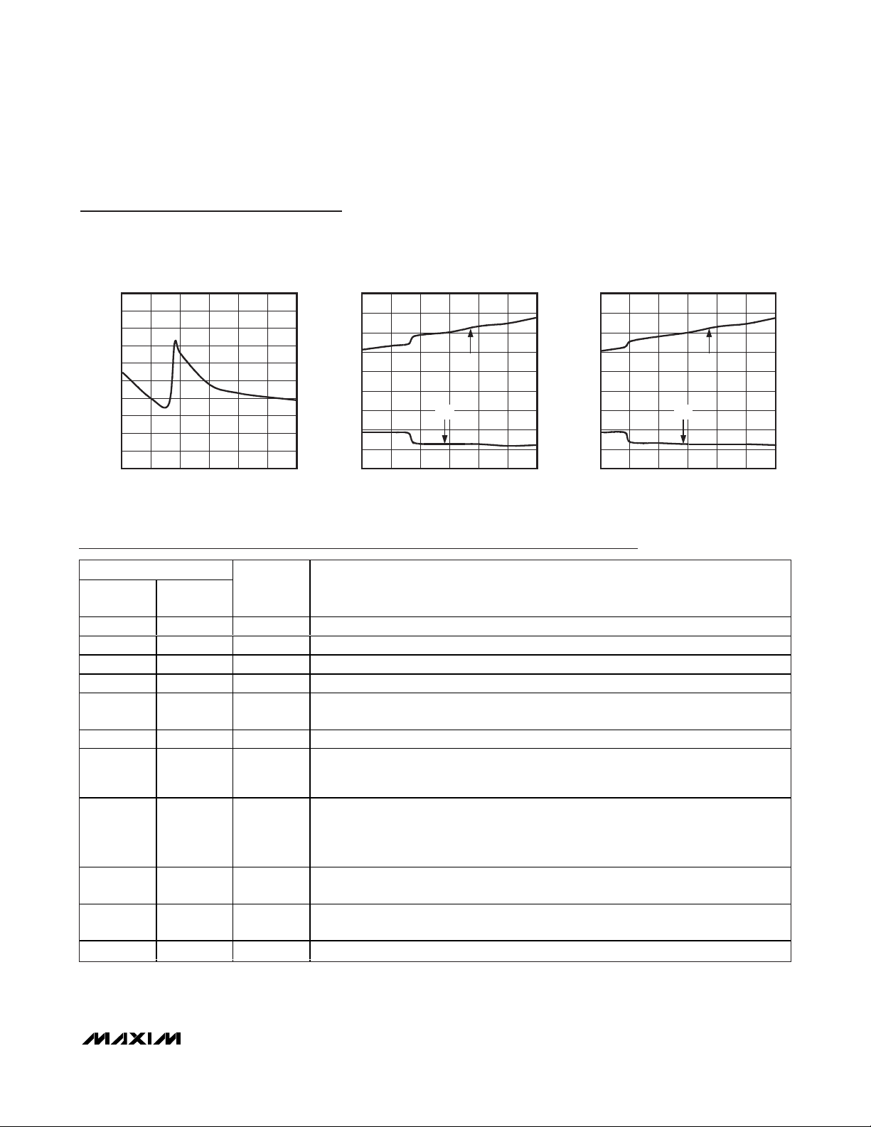
Figure 7 shows a transmitter output when exiting shutdown mode. The transmitter is loaded with 3kΩ in parallel with 1000pF. The transmitter output displays no
ringing or undesirable transients as it comes out of
shutdown, and is enabled only when the magnitude of
V- exceeds approximately -3V.
High Data Rates
The MAX3228E/AE and MAX3229E/AE maintain the RS232 ±5.0V minimum transmitter output voltage even at
high data rates. Figure 8 shows a transmitter loopback
test circuit. Figure 9 shows a loopback test result at
120kbps, and Figure 10 shows the same test at 250kbps.
For Figure 9, the transmitter was driven at 120kbps into
an RS-232 load in parallel with 1000pF. For Figure 10, a
single transmitter was driven at 250kbps, and loaded
with an RS-232 receiver in parallel with 1000pF.
Figure 8. Transmitter Loopback Test Circuit
MAX3229E/AE
5kΩ
R1IN
R1OUT
C2-
C2+
C1-
C1+
V-
V+
V
CC
V
CC
C4
C3
C1
C2
0.1μF
0.1μF
FORCEOFFFORCEON
INVALID
T1OUT
T1IN
GND
V
L
TO POWERMANAGEMENT UNIT
1000pF
V
L
V
L
V
L
V
L
Figure 9. Loopback Test Result at 120kbps
0
R_OUT
T_OUT
T_IN
-5V
5V
0
5V
5V
0
4μs/div
Figure 10. Loopback Test Result at 250kbps
0
-5V
5V
0
5V
5V
0
R_OUT
T_OUT
T_IN
4μs/div
Figure 7. Transmitter Outputs Exiting Shutdown or Powering Up
FORCEON =
FORCEOFF
TOUT
4μs/div
0
2V/div
0
5V/div
±15kV ESD-Protected +2.5V to +5.5V
RS-232 Transceivers in UCSP and WLP
______________________________________________________________________________________ 11
Page 12

MAX3228E/MAX3228AE/MAX3229E/MAX3229AE
UCSP Reliability
The UCSP represents a unique packaging form factor
that may not perform equally to a packaged product
through traditional mechanical reliability tests. CSP reliability is integrally linked to the user’s assembly methods,
circuit board material, and usage environment. The user
should closely review these areas when considering use
of a CSP package. Performance through Operating Life
Test and Moisture Resistance remains uncompromised
as it is primarily determined by the wafer-fabrication
process.
Mechanical stress performance is a greater consideration for a CSP package. CSPs are attached through
direct solder contact to the user’s PC board, foregoing
the inherent stress relief of a packaged product lead
frame. Solder joint contact integrity must be considered.
Table 2 shows the testing done to characterize the CSP
reliability performance. In conclusion, the UCSP is capable of performing reliably through environmental stresses
as indicated by the results in the table. Additional usage
data and recommendations are detailed in the UCSP
application note, which can be found on Maxim’s website at www.maxim-ic.com.
Chip Information
TRANSISTOR COUNT: 698
PROCESS TECHNOLOGY: CMOS
±15kV ESD-Protected +2.5V to +5.5V
RS-232 Transceivers in UCSP and WLP
12 ______________________________________________________________________________________
V
L
MAX3229E/AE
5kΩ
R1IN
R1OUT
TTL/CMOS
C2-
C2+
C1-
C1+
A1 A5
C1
D1
A2
A3
A6
C6
B1
A4
E3
E5
E2
20μA20μA
E1
C5
B5
V-
V+
V
CC
2.5V TO 5.5V
C4
0.1μF
C3
0.1μF
C1
0.1μF
C
BYPASS
C2
0.1μF
0.1μF
0.1μF
FORCEOFFFORCEON
INVALID
T1OUT
T1IN
GND
V
L
TO POWERMANAGEMENT
UNIT
RS-232
V
L
V
L
V
L
1.65V TO 5.5V
V
L
Typical Operating Circuits
(continued)
TEST CONDITIONS DURATION
NO. OF FAILURES PER
SAMPLE SIZE
Temperature Cycle
-35°C to +85°C,
-40°C to +100°C
150 cycles,
900 cycles
0/10,
0/200
Operating Life TA = +70°C 240hr 0/10
Moisture Resistance +20°C to +60°C, 90% RH 240hr 0/10
Low-Temperature Storage -20°C 240hr 0/10
Low-Temperature
Operational
-10°C 24hr 0/10
Solderability 8hr steam age — 0/15
ESD
— 0/5
High-Temperature Operating
Life
T
J
= +150°C 168hr 0/45
Table 2. Reliability Test Data
±2000V, Human Body Model
Page 13

MAX3228E/MAX3228AE/MAX3229E/MAX3229AE
±15kV ESD-Protected +2.5V to +5.5V
RS-232 Transceivers in UCSP and WLP
______________________________________________________________________________________ 13
V
CC
12 3456
C2+ C2-
MAX3228E/AE FON = FORCEON
FOFF = FORCEOFF
INV = INVALID
TOP VIEW
V
L
T1IN
V+ N.C. N.C.
FONN.C. T2IN
N.C.C1+ N.C.
FOFFN.C. R2OUT
C1- N.C. N.C.
N.C.
N.C.
R1OUT
GND
INV
T1OUT T2OUT
R2IN
A
B
C
D
E R1IN
V-
Pin Configurations
Page 14
MAX3228E/MAX3228AE/MAX3229E/MAX3229AE
±15kV ESD-Protected +2.5V to +5.5V
RS-232 Transceivers in UCSP and WLP
14 ______________________________________________________________________________________
V
CC
12 3456
C2+ C2-
MAX3229E/AE FON = FORCEON
FOFF = FORCEOFF
INV = INVALID
TOP VIEW
V
L
T1IN
V+ N.C. N.C.
FONN.C. N.C.
N.C.C1+ N.C.
FOFFN.C. R1OUT
C1- N.C. N.C.
N.C.
N.C.
N.C.
GND
INV
T1OUT N.C.
R1IN
A
B
C
D
E N.C.
V-
Pin Configurations (continued)
Page 15

MAX3228E/MAX3228AE/MAX3229E/MAX3229AE
±15kV ESD-Protected +2.5V to +5.5V
RS-232 Transceivers in UCSP and WLP
______________________________________________________________________________________ 15
PACKAGE TYPE PACKAGE CODE DOCUMENT NO.
6 x 5 UCSP B30-2
21-0123
6 x 5 WLP W302A3-2
21-0016
Package Information
For the latest package outline information and land patterns, go to www.maxim-ic.com/packages.
Page 16

MAX3228E/MAX3228AE/MAX3229E/MAX3229AE
±15kV ESD-Protected +2.5V to +5.5V
RS-232 Transceivers in UCSP and WLP
Maxim cannot assume responsibility for use of any circuitry other than circuitry entirely embodied in a Maxim product. No circuit patent licenses are
implied. Maxim reserves the right to change the circuitry and specifications without notice at any time.
16
____________________Maxim Integrated Products, 120 San Gabriel Drive, Sunnyvale, CA 94086 408-737-7600
© 2008 Maxim Integrated Products is a registered trademark of Maxim Integrated Products, Inc.
Revision History
REVISION
NUMBER
REVISION
DATE
DESCRIPTION PAGES CHANGED
0 8/01 Initial release —
1 5/04 Changed output voltage swing spec 3
2 10/08 Addition of lead-free WLP packaging 1, 5, 6, 7, 15
 Loading...