

Page 1
________________General Description
The MAX3224E/MAX3225E/MAX3226E/MAX3227E/
MAX3244E/MAX3245E are 3V-powered EIA/TIA-232
and V.28/V.24 communications interfaces with automatic shutdown/wakeup features, high data-rate capabilities, and enhanced electrostatic discharge (ESD)
protection. All transmitter outputs and receiver inputs
are protected to ±15kV using IEC 1000-4-2 Air-Gap
Discharge, ±8kV using IEC 1000-4-2 Contact Discharge,
and ±15kV using the Human Body Model.
All devices achieve a 1µA supply current using Maxim’s
revolutionary AutoShutdown Plus™ feature. These
devices automatically enter a low-power shutdown
mode when the RS-232 cable is disconnected or the
transmitters of the connected peripherals are inactive,
and the UART driving the transmitter inputs is inactive
for more than 30 seconds. They turn on again when
they sense a valid transition at any transmitter or receiver input. AutoShutdown Plus saves power without
changes to the existing BIOS or operating system.
The MAX3225E/MAX3227E/MAX3245E also feature
MegaBaud™ operation, guaranteeing 1Mbps for highspeed applications such as communicating with ISDN
modems. The MAX3224E/MAX3226E/MAX3244E guarantee 250kbps operation. The transceivers have a proprietary low-dropout transmitter output stage enabling
true RS-232 performance from a +3.0V to +5.5V supply
with a dual charge pump. The charge pump requires
only four small 0.1µF capacitors for operation from a
3.3V supply. The MAX3224E–MAX3227E feature a logiclevel output (READY) that asserts when the charge
pump is regulating and the device is ready to begin
transmitting.
All devices are available in a space-saving TQFN,
SSOP, and TSSOP (MAX3224E/MAX3225E/MAX3244E/
MAX3245E) packages.
________________________Applications
Notebook, Subnotebook, and Palmtop Computers
Cellular Phones
Battery-Powered Equipment
Hand-Held Equipment
Peripherals
Printers
__Next Generation Device Features
♦ For Space-Constrained Applications:
MAX3228E/MAX3229E: ±15kV ESD-Protected,
+2.5V to +5.5V, RS-232 Transceivers in UCSP
MAX3222E/MAX3232E/MAX3241E
†
/MAX3246E:
±15kV ESD-Protected, Down to 10nA, +3.0V to
+5.5V, Up to 1Mbps, True RS-232 Transceivers
(MAX3246E Available in UCSP™)
♦ For Low-Voltage or Data Cable Applications:
MAX3380E/MAX3381E: +2.35V to +5.5V, 1µA,
2Tx/2Rx RS-232 Transceivers with ±15kV
ESD-Protected I/O and Logic Pins
MAX3224E–MAX3227E/MAX3244E/MAX3245E
†
±15kV ESD-Protected, 1µA, 1Mbps, 3.0V to 5.5V,
RS-232 Transceivers with AutoShutdown Plus
________________________________________________________________ Maxim Integrated Products 1
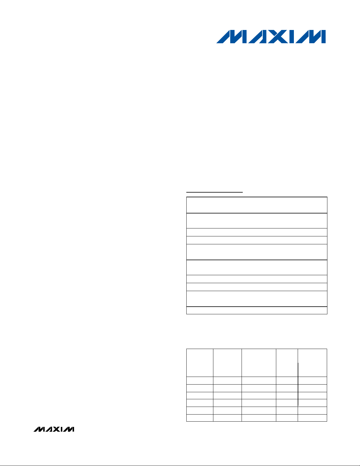
19-1339; Rev 9; 2/07
PART
MAX3224E
MAX3225E
MAX3226E
1/1
2/2
2/2
NO. OF
DRIVERS/
RECEIVERS
READY
OUTPUT
✔
✔
✔
Auto-
Shutdown
Plus
✔
✔
✔
250k
1M
250k
GUARANTEED
DATA RATE
(bps)
MAX3227E
MAX3244E
MAX3245E
3/5
3/5
1/1
✔
—
—
✔
✔
✔
1M
250k
1M
Ordering Information continued at end of data sheet.
*EP = Exposed paddle.
†
Covered by U.S. Patent numbers 4,636,930; 4,679,134; 4,777,577;
4,797,899; 4,809,152; 4,897,774; 4,999,761; 5,649,210; and other
patents pending.
AutoShutdown Plus, MegaBaud, and UCSP are trademarks of
Maxim Integrated Products, Inc.
_____________________ Selector Guide
Ordering Information
For pricing, delivery, and ordering information, please contact Maxim/Dallas Direct! at
1-888-629-4642, or visit Maxim’s website at www.maxim-ic.com.
PART
MAX3224ECTP
MAX3224ECUP
MAX3224ECAP
MAX3224ECPP
MAX3224EETP
MAX3224EEUP
MAX3224EEAP
MAX3224EEPP
MAX3224EAAP
TEMP
RANGE
0°C to +70°C
0°C to +70°C
0°C to +70°C
0°C to +70°C
-40°C to +85°C
-40°C to +85°C
-40°C to +85°C
-40°C to +85°C
-40°C to +125°C
PIN
PKG
20 TQFN-
EP*
20 TSSOP —
20 SSOP —
20 Plastic
DIP
20 TQFN-
EP*
20 TSSOP —
20 SSOP —
20 Plastic
DIP
20 SSOP —
PKG
CODE
T2055-5
—
T2055-5
—
Page 2
MAX3224E–MAX3227E/MAX3244E/MAX3245E
†
±15kV ESD-Protected, 1µA, 1Mbps, 3.0V to 5.5V,
RS-232 Transceivers with AutoShutdown Plus
2 _______________________________________________________________________________________
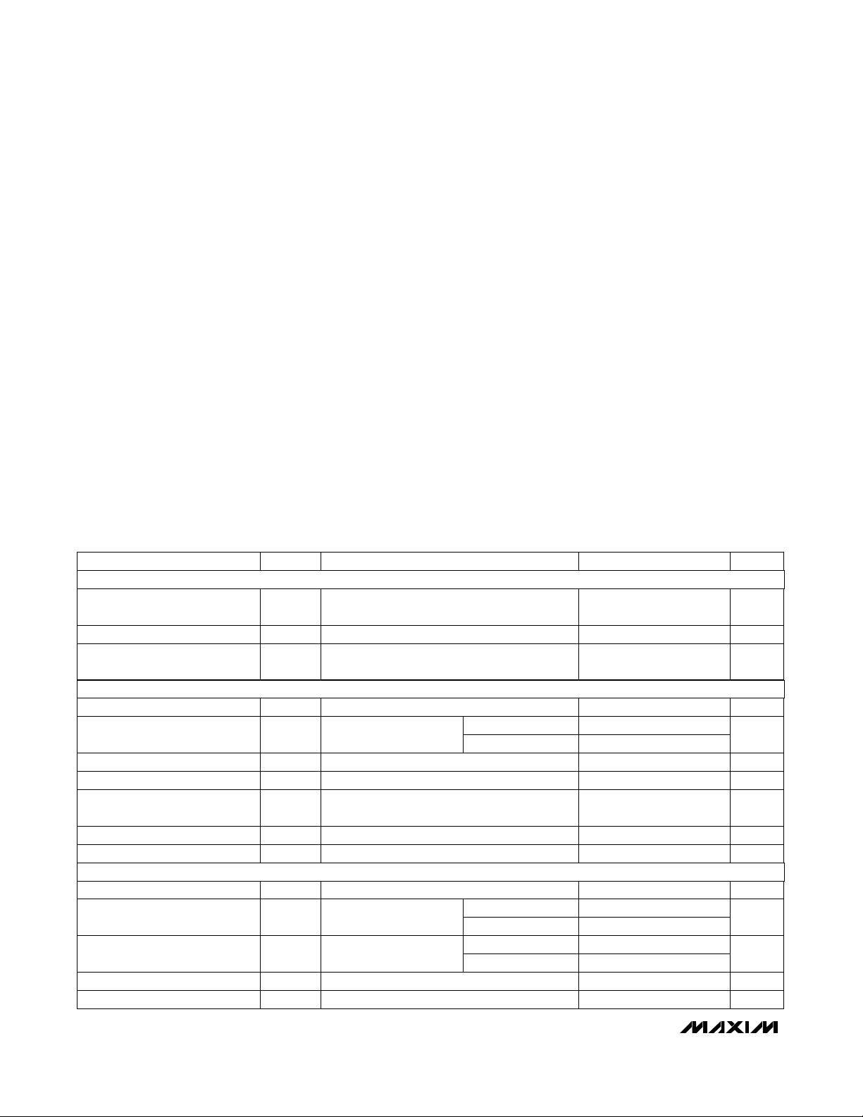
ABSOLUTE MAXIMUM RATINGS
ELECTRICAL CHARACTERISTICS
(VCC= +3V to +5.5V, C1–C4 = 0.1µF, tested at 3.3V ±10%; C1= 0.047µF, C2–C4 = 0.33µF, tested at 5.0V ±10%; TA= T
MIN
to T
MAX
,
unless otherwise noted. Typical values are at T
A
= +25°C.)
Stresses beyond those listed under “Absolute Maximum Ratings” may cause permanent damage to the device. These are stress ratings only, and functional
operation of the device at these or any other conditions beyond those indicated in the operational sections of the specifications is not implied. Exposure to
absolute maximum rating conditions for extended periods may affect device reliability.
VCCto GND..............................................................-0.3V to +6V
V+ to GND (Note 1) ..................................................-0.3V to +7V
V- to GND (Note 1) ...................................................+0.3V to -7V
V+ +⏐V-⏐(Note 1) ................................................................+13V
Input Voltages
T_IN, FORCEON, FORCEOFF to GND ................ -0.3V to +6V
R_IN to GND ....................................................................±25V
Output Voltages
T_OUT to GND.............................................................±13.2V
R_OUT, INVALID, READY to GND .........-0.3V to (V
CC
+ 0.3V)
Short-Circuit Duration
T_OUT to GND .......................................................Continuous
Continuous Power Dissipation (T
A
= +70°C)
16-Pin SSOP (derate 7.14mW/°C above +70°C) .........571mW
16-Pin TSSOP (derate 9.4mW/°C above +70°C) ......754.7mW
16-Pin TQFN (derate 20.8mW/°C above +70°C) ....1666.7mW
20-Pin TQFN (derate 21.3mW/°C above +70°C) ....1702.1mW
20-Pin Plastic DIP (derate 11.11mW/°C above +70°C) ...889mW
20-Pin SSOP (derate 8.00mW/°C above +70°C) .........640mW
20-Pin TSSOP (derate 10.9mW/°C above +70°C) .......879mW
28-Pin Wide SO (derate 12.5mW/°C above +70°C)............1W
28-Pin SSOP (derate 9.52mW/°C above +70°C) .........762mW
28-Pin TSSOP (derate 12.8mW/°C above +70°C) .......1026mW
36-Pin TQFN (derate 26.3mW/°C above +70°C)...........2105mW
Operating Temperature Ranges
MAX32_ _EC_ _ .................................................0°C to +70°C
MAX32_ _EE_ _................................................-40°C to +85°C
MAX32_ _EAA_..............................................-40°C to +125°C
Storage Temperature Range .............................-65°C to +160°C
Lead Temperature (soldering, 10s) .................................+300°C
Note 1: V+ and V- can have maximum magnitudes of 7V, but their absolute difference cannot exceed 13V.
VCC= 5.0V
FORCEON = GND, FORCEOFF = VCC,
all R_IN idle, all T_IN idle
TA= +25°C
VCC= 3.3V
T_IN, FORCEON,
FORCEOFF
CONDITIONS
kΩ357Input Resistance
V0.5Input Hysteresis
1.8 2.4
V
1.5 2.4
Input Threshold High
0.8 1.5
V
0.6 1.2
Input Threshold Low
V-25 +25Input Voltage Range
V
VCC- 0.6 VCC- 0.1
Output Voltage High
V0.4Output Voltage Low
µA110Supply Current, Shutdown
µA110
Supply Current,
AutoShutDown Plus
µA±0.05 ±10Output Leakage Current
µA±0.01 ±1
Transmitter Input Hysteresis V0.5
V
2.4
Input Logic Threshold High
mA0.3 1
Supply Current,
AutoShutDown Plus Disabled
V0.8Input Logic Threshold Low
2
UNITSMIN TYP MAXSYMBOLPARAMETER
FORCEOFF = GND
TA= +25°C
VCC= 5.0V
VCC= 3.3V
TA= +25°C
R_OUT (MAX3244E/MAX3245E), receivers
disabled
T_IN, FORCEON, FORCEOFF
VCC= 5.0V
FORCEON = FORCEOFF = VCC, no load
T_IN, FORCEON, FORCEOFF
I
OUT
= -1.0mA
VCC= 3.3V
I
OUT
= 1.6mA
DC CHARACTERISTICS (VCC= 3.3V or 5.0V, TA= +25°C)
LOGIC INPUTS AND RECEIVER OUTPUTS
RECEIVER INPUTS
Input Leakage Current
Page 3
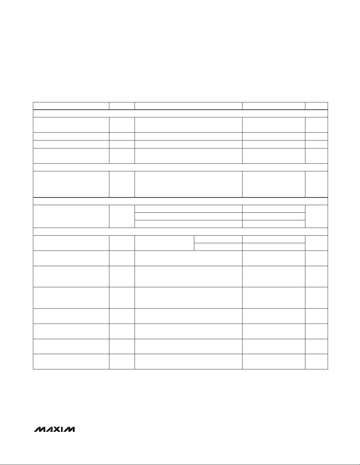
MAX3224E–MAX3227E/MAX3244E/MAX3245E
†
±15kV ESD-Protected, 1µA, 1Mbps, 3.0V to 5.5V,
RS-232 Transceivers with AutoShutdown Plus
_______________________________________________________________________________________ 3
ELECTRICAL CHARACTERISTICS (continued)
(VCC= +3V to +5.5V, C1–C4 = 0.1µF, tested at 3.3V ±10%; C1= 0.047µF, C2–C4 = 0.33µF, tested at 5.0V ±10%; TA= T
MIN
to T
MAX
,
unless otherwise noted. Typical values are at T
A
= +25°C.)
CONDITIONS
Ω300 10MOutput Resistance
V±5 ±5.4Output Voltage Swing
UNITSMIN TYP MAXSYMBOLPARAMETER
Figure 4a
T1IN = T2IN = GND, T3IN = VCC,
T3OUT loaded with 3kΩ to GND,
T1OUT and T2OUT loaded with
2.5mA each
s15 30 60t
AUTOSHDN
Receiver or Transmitter Edge to
Transmitters Shutdown
µs100t
WU
Receiver or Transmitter Edge to
Transmitters Enabled
µs30t
INVL
Receiver Positive or Negative
Threshold to INVALID Low
µs1t
INVH
Receiver Positive or Negative
Threshold to INVALID High
V
V
CC
- 0.6
INVALID, READY
Output Voltage High
(MAX3224E–MAX3227E)
V0.4
INVALID, READY
Output Voltage Low
(MAX3224E–MAX3227E)
V-0.3 +0.3
Receiver Input Threshold to
INVALID Output Low
-2.7
V
2.7
Receiver Input Threshold to
INVALID Output High
±15
±8R_IN, T_OUT kV
±15
V±5Transmitter Output Voltage
µA±25Output Leakage Current
±60 mAOutput Short-Circuit Current
VCC= V+ = V- = 0, transmitter outputs = ±2V
All transmitter outputs loaded with 3kΩ to
ground
VCC= 5V, Figure 5b (Note 2)
VCC= 5V, Figure 5b (Note 2)
VCC= 5V, Figure 4b
VCC= 5V, Figure 4b
I
OUT
= -1.0mA
I
OUT
= -1.6mA
Figure 4a
Negative threshold
Positive threshold
Human Body Model
VCC= 0 or 3V to 5.5V, V
OUT
= ±12V,
Transmitters disabled
IEC1000-4-2 Contact Discharge
IEC1000-4-2 Air Discharge
TRANSMITTER OUTPUTS
MOUSE DRIVEABILITY (MAX3244E/MAX3245E)
ESD PROTECTION
AutoShutdown Plus (FORCEON = GND, FORCEOFF = VCC)
Page 4
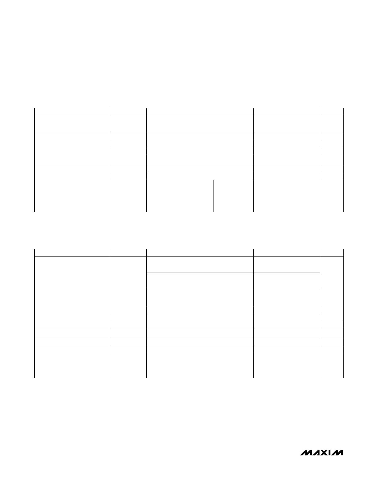
MAX3224E–MAX3227E/MAX3244E/MAX3245E
†
±15kV ESD-Protected, 1µA, 1Mbps, 3.0V to 5.5V,
RS-232 Transceivers with AutoShutdown Plus
4 _______________________________________________________________________________________
TIMING CHARACTERISTICS—MAX3224E/MAX3226E/MAX3244E
(VCC= +3V to +5.5V, C1–C4 = 0.1µF, tested at 3.3V ±10%; C1= 0.047µF, C2–C4 = 0.33µF, tested at 5.0V ±10%; TA= T
MIN
to T
MAX
,
unless otherwise noted. Typical values are at T
A
= +25°C.)
TIMING CHARACTERISTICS—MAX3225E/MAX3227E/MAX3245E
(VCC= +3V to +5.5V, C1–C4 = 0.1µF, tested at 3.3V ±10%; C1= 0.047µF, C2–C4 = 0.33µF, tested at 5.0V ±10%; TA= T
MIN
to T
MAX
,
unless otherwise noted. Typical values are at T
A
= +25°C.)
Note 2: A transmitter/receiver edge is defined as a transition through the transmitter/receiver input logic thresholds.
Note 3: Transmitter skew is measured at the transmitter zero cross points.
CL= 150pF
to 1000pF
R_IN to R_OUT, CL= 150pF
RL= 3kΩ, CL= 1000pF,
one transmitter switching
VCC= 3.3V, TA= +25°C,
RL= 3kΩ to 7kΩ,
measured from +3V to -3V
or -3V to +3V, one transmitter switching
Normal operation (MAX3244E only)
Normal operation (MAX3244E only)
(Note 3)
CONDITIONS
0.15t
PLH
µs
0.15t
PHL
kbps250Maximum Data Rate
Receiver Propagation Delay
V/µs630Transition-Region Slew Rate
ns200Receiver Output Enable Time
ns200Receiver Output Disable Time
ns100
⏐
t
PHL
- t
PLH
⏐
Transmitter Skew
ns50
⏐
t
PHL
- t
PLH ⏐
Receiver Skew
UNITSMIN TYP MAXSYMBOLPARAMETER
VCC= 4.5V to 5.5V, RL= 3kΩ,
C
L
= 1000pF, one transmitter switching
VCC= 3.0V to 4.5V, RL= 3kΩ,
CL= 250pF, one transmitter switching
RL= 3kΩ, CL= 1000pF,
one transmitter switching
VCC= 3.3V, TA= +25°C,
RL= 3kΩ to 7kΩ, CL= 150pF to 1000pF,
measured from +3V to -3V or -3V to +3V,
one transmitter switching
(Note 3)
R_IN to R_OUT, CL= 150pF
Normal operation (MAX3245E only)
Normal operation (MAX3245E only)
CONDITIONS
1000
1000
kbps
250
Maximum Data Rate
V/µs24 150Transition-Region Slew Rate
ns50
⏐
t
PHL
- t
PLH
⏐
Receiver Skew
ns25
⏐
t
PHL
- t
PLH
⏐
Transmitter Skew
µs
0.15t
PHL
Receiver Propagation Delay
0.15t
PLH
ns200Receiver Output Enable Time
ns200Receiver Output Disable Time
UNITSMIN TYP MAXSYMBOLPARAMETER
Page 5
MAX3224E–MAX3227E/MAX3244E/MAX3245E
†
±15kV ESD-Protected, 1µA, 1Mbps, 3.0V to 5.5V,
RS-232 Transceivers with AutoShutdown Plus
_______________________________________________________________________________________ 5
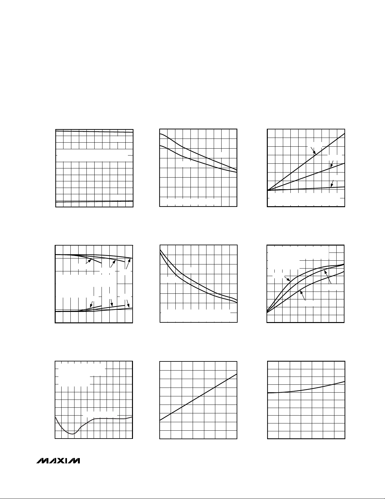
__________________________________________Typical Operating Characteristics
(VCC= +3.3V, 250kbps data rate, 0.1µF capacitors, all transmitters loaded with 3kΩ and CL, TA= +25°C, unless otherwise noted.)
0
200
180
160
140
120
100
80
60
40
20
-40 0 20-20 406080100
MAX3224E–MAX3227E
READY TURN-OFF TIME
vs. TEMPERATURE
MAX3224-7/44/45E-09
TEMPERATURE (°C)
READY TURN-OFF TIME (ns)
MAX3224E/MAX3226E
TRANSMITTER OUTPUT VOLTAGE
6
5
4
3
2
1
0
-1
-2
-3
-4
TRANSMITTER OUTPUT VOLTAGE (V)
-5
-6
7.5
5.0
2.5
0
-2.5
-5.0
TRANSMITTER OUTPUT VOLTAGE (V)
-7.5
50
45
40
35
30
25
20
15
TRANSMITTER SKEW (ns)
10
5
0
vs. LOAD CAPACITANCE
T1 TRANSMITTING AT 250kbps
T2 (MAX3224E) TRANSMITTING AT 15.6kbps
0 10002000300040005000
LOAD CAPACITANCE (pF)
MAX3225E/MAX3227E
TRANSMITTER OUTPUT VOLTAGE
vs. LOAD CAPACITANCE
2Mbps
1 TRANSMITTER AT FULL DATA RATE
1 TRANSMITTER AT 1/16 DATA RATE
(MAX3225E)
LOAD = 3kΩ + C
01000500 1500 2000 2500
L
LOAD CAPACITANCE (pF)
MAX3225E/MAX3227E
TRANSMITTER SKEW
vs. LOAD CAPACITANCE
1 TRANSMITTER AT 512kbps
1 TRANSMITTER AT 30kbps
(MAX3225E)
LOAD = 3kΩ + C
0 1000500 1500 2000 2500 3000
L
AVERAGE: 10 PARTS
LOAD CAPACITANCE (pF)
2Mbps
V
V
1.5Mbps
1.5Mbps
OUT+
OUT-
1Mbps
1Mbps
16
14
12
MAX3224-7/44/45E-01
10
SLEW RATE (V/μs)
80
70
60
MAX3224-7/44/45E-04
50
40
30
SLEW RATE (V/μs)
20
10
MAX3224-7/44/45E-07
READY TURN-ON TIME (μs)
MAX3224E/MAX3226E
SLEW RATE vs. LOAD CAPACITANCE
-SLEW
8
6
4
2
0
0 1000 2000 3000 4000 5000
+SLEW
FOR DATA RATES UP TO 250kbps
LOAD CAPACITANCE (pF)
MAX3225E/MAX3227E
SLEW RATE vs. LOAD CAPACITANCE
-SLEW
+SLEW
1 TRANSMITTER AT 1Mbps
1 TRANSMITTER AT 62.5kbps (MAX3225E)
0
0 500 1000 1500 2000 2500
LOAD CAPACITANCE (pF)
MAX3224E–MAX3227E
READY TURN-ON TIME
vs. TEMPERATURE
38
36
34
32
30
28
26
24
22
20
-40 0 20-20 40 60 80 100
TEMPERATURE (°C)
45
40
35
MAX3224-7/44/45E-02
30
25
20
15
SUPPLY CURRENT (mA)
10
5
0
100
90
80
MAX3224-7/44/45E-05
70
60
50
40
30
SUPPLY CURRENT (mA)
20
10
0
MAX3224-7/44/45E-08
MAX3224E/MAX3226E
OPERATING SUPPLY CURRENT
vs. LOAD CAPACITANCE
250kbps
120kbps
20kbps
T1 TRANSMITTING AT 250kbps
T2 (MAX3224E) TRANSMITTING AT 15.6kbps
020001000 3000 4000 5000
LOAD CAPACITANCE (pF)
MAX3225E/MAX3227E
OPERATING SUPPLY CURRENT
vs. LOAD CAPACITANCE
1 TRANSMITTER AT FULL DATA RATE
1 TRANSMITTER AT 1/16 DATA RATE
(MAX3225E)
LOAD = 3kΩ + C
2Mbps
0 500 1000 1500 2000 2500
L
1.5Mbps
1Mbps
LOAD CAPACITANCE (pF)
MAX3224-7/44/45E-03
MAX3224-7/44/45E-06
Page 6
MAX3224E–MAX3227E/MAX3244E/MAX3245E
†
±15kV ESD-Protected, 1µA, 1Mbps, 3.0V to 5.5V,
RS-232 Transceivers with AutoShutdown Plus
6 _______________________________________________________________________________________
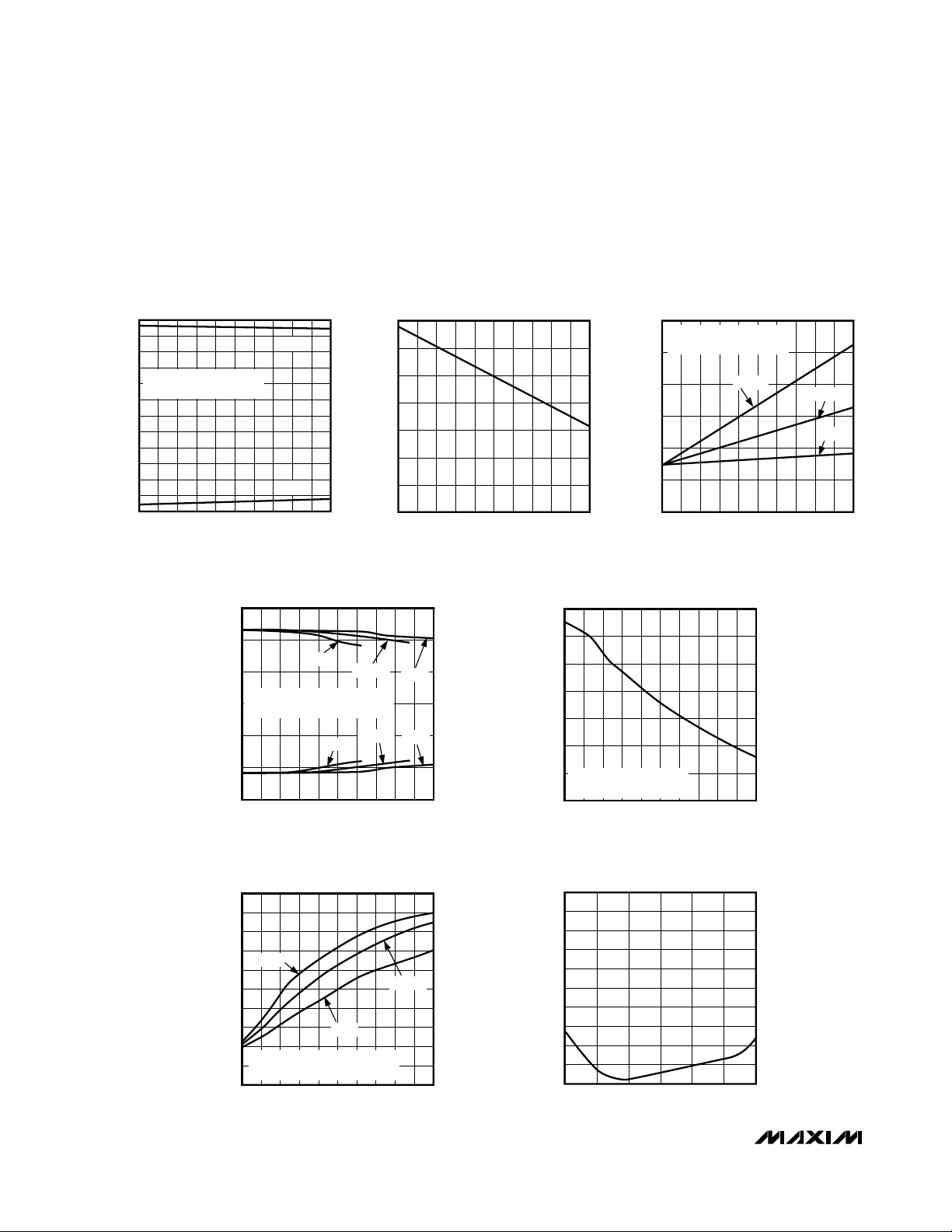
_____________________________Typical Operating Characteristics (continued)
(V
CC
= +3.3V, 250kbps data rate, 0.1µF capacitors, all transmitters loaded with 3kΩ and CL, TA= +25°C, unless otherwise noted.)
-6
-5
-4
-3
-2
-1
0
1
2
3
4
5
6
0 1000 2000 3000 4000 5000
MAX3244E
TRANSMITTER OUTPUT VOLTAGE
vs. LOAD CAPACITANCE
MAX3224-7/44/45E-10
LOAD CAPACITANCE (pF)
TRANSMITTER OUTPUT VOLTAGE (V)
1 TRANSMITTER AT 250kbps
2 TRANSMITTERS AT 15.6kbps
V
OUT+
V
OUT-
0
4
2
8
6
12
10
14
0 1000 2000 3000 4000 5000
MAX3244E
SLEW RATE vs. LOAD CAPACITANCE
MAX3224-7/44/45E-11
LOAD CAPACITANCE (pF)
SLEW RATE (V/
μ
s)
0
30
20
10
40
50
60
0 20001000 3000 4000 5000
MAX3244E
OPERATING SUPPLY CURRENT
vs. LOAD CAPACITANCE
MAX3224-7/44/45E-12
LOAD CAPACITANCE (pF)
SUPPLY CURRENT (mA)
250kbps
120kbps
20kbps
1 TRANSMITTER AT 250kbps
2 TRANSMITTERS AT 15.6kbps
-7.5
0
-2.5
-5.0
2.5
5.0
7.5
0 800400 1200 1600 2000
MAX3245E
TRANSMITTER OUTPUT VOLTAGE
vs. LOAD CAPACITANCE
MAX3224-7/44/45E-13
LOAD CAPACITANCE (pF)
TRANSMITTER OUTPUT VOLTAGE (V)
2Mbps
2Mbps
1.5Mbps
1.5Mbps
1Mbps
1Mbps
1 TRANSMITTER AT FULL DATA RATE
2 TRANSMITTERS AT 1/16 DATA RATE
0
20
10
40
30
60
50
70
90
80
100
0 400 800 1200 1600 2000
MAX3245E
OPERATING SUPPLY CURRENT
vs. LOAD CAPACITANCE
MAX3224-7/44/45E-15
LOAD CAPACITANCE (pF)
SUPPLY CURRENT (mA)
2Mbps
1.5Mbps
1Mbps
1 TRANSMITTER AT FULL DATA RATE
2 TRANSMITTERS AT 1/16 DATA RATE
0
20
10
40
30
60
50
70
0 400 800 1200 1600 2000
MAX3245E
SLEW RATE vs. LOAD CAPACITANCE
MAX3224-7/44/45E-14
LOAD CAPACITANCE (pF)
SLEW RATE (V/
μ
s)
1 TRANSMITTER AT 1Mbps
2 TRANSMITTERS AT 62.5kbps
0
15
10
5
20
25
30
35
40
45
50
0 1000 2000 3000
MAX3245E
TRANSMITT SKEW
vs. LOAD CAPACITANCE
MAX3224-7/44/45E-16
LOAD CAPACITANCE (pF)
TRANSMITTER SKEW (ns)
Page 7
MAX3224E–MAX3227E/MAX3244E/MAX3245E
†
±15kV ESD-Protected, 1µA, 1Mbps, 3.0V to 5.5V,
RS-232 Transceivers with AutoShutdown Plus
_______________________________________________________________________________________ 7
______________________________________________________________ Pin Description
PIN
MAX3224E
MAX3225E
TQFN
19 1 14 1 — — READY
1 2 16 2 28 31 C1+
20 3 15 3 27 30
2 4 1 4 24 26 C1-
3 5 2 5 1 33 C2+
DIP/
SSOP/
TSSOP
MAX3226E
MAX3227E
TQFN
SSOP/
TSSOP
MAX3244E
MAX3245E
SO/ SSOP/ TSSOP
MAX3245E
(TQFN)
NAME FUNCTION
Ready to Transmit Output,
active-high. READY is
enabled high when V- goes
below -4V and the device is
ready to transmit.
Positive Terminal of VoltageDoubler Charge-Pump
Capacitor
V+
+5.5V generated by the
charge pump
Negative Terminal of
Voltage-Doubler ChargePump Capacitor
Positive Terminal of
Inverting Charge-Pump
Capacitor
4 6 3 6 2 34 C2-
5747 3 35 V-
6, 15 8, 17 10 13 9, 10, 11 7, 8, 9 T_OUT
7, 14 9, 16 5 8 4-8 1-5 R_IN
8, 13 10, 15 6 9
911710
15-19
21 23 INVALID
15, 16, 17,
19, 20
R_OUT
Negative Terminal of
Inverting Charge-Pump
Capacitor
-5.5V Generated by the
Charge Pump
RS-232 Transmitter Outputs
RS-232 Receiver Inputs
TTL/CMOS Receiver
Outputs
Valid Signal Detector
Output, active low. A logic
high indicates that a valid
RS-232 level is present on a
receiver input.
Page 8
MAX3224E–MAX3227E/MAX3244E/MAX3245E
†
±15kV ESD-Protected, 1µA, 1Mbps 3.0V to 5.5V,
RS-232 Transceivers with AutoShutdown Plus
8 _______________________________________________________________________________________
______________________________________________________________ Pin Description
_______________Detailed Description
Dual Charge-Pump Voltage Converter
The MAX3224E–MAX3227E/MAX3244E/MAX3245E’s
internal power supply consists of a regulated dual
charge pump that provides output voltages of +5.5V
(doubling charge pump) and -5.5V (inverting charge
pump), over the +3.0V to +5.5V range. The charge
pump operates in discontinuous mode: if the output
voltages are less than 5.5V, the charge pump is
enabled; if the output voltages exceed 5.5V, the
charge-pump is disabled. Each charge pump requires
a flying capacitor (C1, C2) and a reservoir capacitor
(C3, C4) to generate the V+ and V- supplies.
The READY output (MAX3224E–MAX3227E) is low
when the charge pumps are disabled in shutdown
mode. The READY signal asserts high when V- goes
below -4V.
PIN
MAX3224E
MAX3225E
TQFN
10, 11 12, 13 8 11 12-14 11, 12, 13 T_IN
12 14 9 12 23 25 FORCEON
16 18 11 14 25 27
17 19 12 15 26 29
18 20 13 16 22 24
— — — — 20 21 R2OUTB
DIP/
SSOP/
TSSOP
MAX3226E
MAX3227E
TQFN
SSOP/
TSSOP
MAX3244E
MAX3245E
DIP/ SSOP/ TSSOP
MAX3245E
TQFN
NAME
GND
V
CC
FORCEOFF
FUNCTION
TTL/CMOS Transmitter
Inputs
Force-On Input, Active High.
Drive high to override
AutoShutdown Plus, keeping
transmitters and receivers
on (FORCEOFF must be
high) (Table 1).
Ground
+3.0V to +5.5V Single
Supply Voltage
Force-Off Input, Active Low.
Drive low to shut down
transmitters, receivers
(except R2OUTB), and
charge pump. This
overrides AutoShutdown
Plus and FORCEON (Table
1).
TTL/CMOS Noninverting
Complementary Receiver
Outputs. Always active.
———— —
EP — EP — — EP EP
6, 10, 14,
18, 22, 28,
32, 36
N.C.
No Connection. Not
internally connected.
Exposed Paddle. Solder the
exposed paddle to the
ground plane or leave
unconnected.
Page 9

MAX3224E–MAX3227E/MAX3244E/MAX3245E
†
±15kV ESD-Protected, 1µA, 1Mbps 3.0V to 5.5V,
RS-232 Transceivers with AutoShutdown Plus
_______________________________________________________________________________________ 9
RS-232 Transmitters
The transmitters are inverting level translators that
convert CMOS-logic levels to 5.0V EIA/TIA-232 levels.
The MAX3224E/MAX3226E/MAX3244E guarantee a
250kbps data rate (1Mbps, for the MAX3225E/MAX3227E/
MAX3245E) with worst-case loads of 3kΩ in parallel with
1000pF, providing compatibility with PC-to-PC communication software (such as LapLink™). Transmitters
can be paralleled to drive multiple receivers. Figure 1
shows a complete system connection.
When FORCEOFF is driven to ground or when the AutoShutdown Plus circuitry senses that all receiver and
transmitter inputs are inactive for more than 30s, the
transmitters are disabled and the outputs go into a highimpedance state. When powered off or shut down, the
outputs can be driven to ±12V. The transmitter inputs
do not have pullup resistors. Connect unused inputs to
GND or V
CC
.
Figure 1. Interface Under Control of PMU
Figure 2. The MAX3244E/MAX3245E detect RS-232 activity
when the UART and interface are shut down.
LapLink is a trademark of Traveling Software.
V
POWERMANAGEMENT
UNIT OR
KEYBOARD
CONTROLLER
FORCEOFF
FORCEON
INVALID
MAX3244E
MAX3245E
V
PROTECTION
DIODE
CC
Rx
CC
PREVIOUS
RS-232
I
I/O
CPU
CHIP
WITH
UART
RS-232
UART
GND
Tx
SHDN = GND
5kΩ
a) OLDER RS-232: POWERED-DOWN UART DRAWS CURRENT FROM ACTIVE
RECEIVER OUTPUT IN SHUTDOWN.
V
CC
TO
LOGIC
μP
TRANSITION
DETECTOR
I
PROTECTION
DIODE
V
CC
Rx
UART
Tx
GND
R2OUTB
R2OUT
THREE-STATED
T1IN
FORCEOFF = GND
MAX3244E
MAX3245E
5kΩ
b) NEW MAX3244E/MAX3245E: IN SHUTDOWN, R2OUTB IS USED TO MONITOR
EXTERNAL DEVICES AND R2OUT IS THREE STATED, ELIMINATING A CURRENT
PATH THROUGH THE UART'S PROTECTION DIODE.
R2IN
T1OUT
Page 10

MAX3224E–MAX3227E/MAX3244E/MAX3245E
†
±15kV ESD-Protected, 1µA, 1Mbps 3.0V to 5.5V,
RS-232 Transceivers with AutoShutdown Plus
10 ______________________________________________________________________________________
RS-232 Receivers
The receivers convert RS-232 signals to CMOS-logic
output levels. The MAX3224E–MAX3227E feature
inverting outputs that always remain active (Table 1).
The MAX3244E/MAX3245E have inverting three-state
outputs that are high impedance when shut down
(FORCEOFF = GND) (Table 1).
The MAX3244E/MAX3245E feature an extra, always
active, noninverting output, R2OUTB. R2OUTB output
monitors receiver activity while the other receivers are
high impedance, allowing ring indicator applications to
be monitored without forward biasing other devices
connected to the receiver outputs. This is ideal for systems where V
CC
is set to ground in shutdown to
accommodate peripherals such as UARTs (Figure 2).
The MAX3224E–MAX3227E/MAX3244E/MAX3245E feature an INVALID output that is enabled low when no
valid RS-232 voltage levels have been detected on all
receiver inputs. Because INVALID indicates the receiver input’s condition, it is independent of FORCEON and
FORCEOFF states (Figures 3 and 4).
AutoShutdown Plus Mode
The MAX3224E–MAX3227E/MAX3244E/MAX3245E
achieve a 1µA supplycurrent with Maxim’s AutoShutdown
Plus feature, which operates when FORCEOFF is high
and a FORCEON is low. When these devices do not
sense a valid signal transition on any receiver and transmitter input for 30s, the on-board charge pumps are
shut down, reducing supply current to 1µA. This occurs
if the RS-232 cable is disconnected or if the connected
Table 1. Output Control Truth Table
OPERATION
STATUS
FORCEON
FORCEOFF
VALID
RECEIVER
LEVEL
RECEIVER OR
TRANSMITTER
EDGE WITHIN
30s
T_OUT
R_OUT
(MAX3224E/
MAX3225E/
MAX3226E/
MAX3227E)
R_OUT
(MAX3244E/
MAX3245E)
R2OUTB
(MAX3244E/
MAX3245E)
Shutdown
(Forced Off)
X 0 X X High-Z Active High-Z Active
Normal
Operation
(Forced On)
1 1 X X Active Active Active Active
Normal
Operation
(AutoShutdown
Plus)
0 1 X Yes Active Active Active Active
Shutdown (AutoShutdown Plus)
0 1 X No High-Z Active Active Active
Normal
Operation
INVALID*
1 Yes X Active Active Active Active
Normal
Operation
INVALID*
1 X Yes Active Active Active Active
Shutdown
INVALID*
1 No No High-Z Active Active Active
Normal
Operation
(AutoShutdown)
INVALID* INVALID**
Yes X Active Active Active Active
Shutdown
(AutoShutdown)
INVALID* INVALID**
No X High-Z Active High-Z Active
X = Don’t care
*
INVALID
connected to FORCEON
**
INVALID
connected to FORCEON and
FORCEOFF
Page 11

MAX3224E–MAX3227E/MAX3244E/MAX3245E
†
±15kV ESD-Protected, 1µA, 1Mbps 3.0V to 5.5V,
RS-232 Transceivers with AutoShutdown Plus
______________________________________________________________________________________ 11
peripheral transmitters are turned off, and the UART driving the transmitter inputs is inactive. The system turns
on again when a valid transition is applied to any
RS-232 receiver or transmitter input. As a result, the system saves power without changes to the existing BIOS
or operating system.
Figures 3a and 3b depict valid and invalid RS-232
receiver voltage levels. INVALID indicates the receiver
input’s condition, and is independent of FORCEON and
FORCEOFF states. Figure 3 and Tables 1 and 2 summarize the operating modes of the MAX3224E–
MAX3227E/MAX3244E/MAX3245E. FORCEON and
FORCEOFF override AutoShutdown Plus circuitry.
When neither control is asserted, the IC selects
between these states automatically based on the last
receiver or transmitter input edge received.
When shut down, the device’s charge pumps turn off,
V+ is pulled to VCC, V- is pulled to ground, the transmitter outputs are high impedance, and READY
(MAX3224E–MAX3227E) is driven low. The time
required to exit shutdown is typically 100µs (Figure 8).
By connecting FORCEON to INVALID, the MAX3224E–
MAX3227E/MAX3244E/MAX3245E shut down when no
valid receiver level and no receiver or transmitter edge is
detected for 30s, and wake up when a valid receiver
level or receiver or transmitter edge is detected.
Figure 3a.
INVALID
Functional Diagram,
INVALID
Low
Figure 3b.
INVALID
Functional Diagram,
INVALID
High
Figure 3c. AutoShutdown Plus Logic
Figure 3d. Power-Down Logic
Figure 4a. Receiver Positive/Negative Thresholds for
INVALID
RS-232 SIGNAL
PRESENT AT ANY
RECEIVER INPUT
INVALID OUTPUT
Yes High
No Low
Table 2. INVALID Truth Table
+0.3V
R_IN
-0.3V
INVALID ASSERTED IF ALL RECEIVER INPUTS ARE BETWEEN +0.3V AND -0.3V FOR
AT LEAST 30μs.
+2.7V
R_IN
-2.7V
INVALID DEASSERTED IF ANY RECEIVER INPUT HAS BEEN BETWEEN +2.7V AND -2.7V
FOR LESS THAN 30μs.
30µs
TIMER
R
30µs
TIMER
R
INVALID
INVALID
EDGE
T_IN
DETECT
EDGE
R_IN
DETECT
FORCEON
FORCEOFF
FORCEON
AUTOSHDN
* POWERDOWN IS ONLY AN INTERNAL SIGNAL.
IT CONTROLS THE OPERATIONAL STATUS OF
THE TRANSMITTERS AND THE POWER SUPPLIES.
FORCEOFF
S
30s
TIMER
R
AUTOSHDN
POWERDOWN*
INVALID HIGH
+2.7V
INDETERMINATE
+0.3V
0
-0.3V
RECEIVER INPUT LEVELS
-2.7V
INVALID LOW
INDETERMINATE
INVALID HIGH
Page 12

MAX3224E–MAX3227E/MAX3244E/MAX3245E
†
±15kV ESD-Protected, 1µA, 1Mbps 3.0V to 5.5V,
RS-232 Transceivers with AutoShutdown Plus
12 ______________________________________________________________________________________
By connecting FORCEON and FORCEOFF to INVALID,
the MAX3224E–MAX3227E/MAX3244E/MAX3245E shut
down when no valid receiver level is detected and
wake up when a valid receiver level is detected (same
functionality as AutoShutdown feature on MAX3221E/
MAX3223E/MAX3243E).
A mouse or other system with AutoShutdown Plus may
need time to wake up. Figure 5 shows a circuit that
forces the transmitters on for 100ms, allowing enough
time for the other system to realize that the MAX3244E/
MAX3245E is awake. If the other system outputs valid
RS-232 signal transitions within that time, the RS-232
ports on both systems remain enabled.
Software-Controlled Shutdown
If direct software control is desired, use INVALID to
indicate DTR or ring indicator signal. Tie FORCEOFF
and FORCEON together to bypass the AutoShutdown
Plus so the line acts like a SHDN input.
±15kV ESD Protection
As with all Maxim devices, ESD-protection structures are
incorporated on all pins to protect against electrostatic
discharges encountered during handling and assembly.
The driver outputs and receiver inputs of the
MAX3224E–MAX3227E/MAX3244E/MAX3245E have extra
protection against static electricity. Maxim’s engineers
have developed state-of-the-art structures to protect
Figure 4b. AutoShutdown Plus,
INVALID,
and READY Timing Diagram
Figure 5. AutoShutdown Plus Initial Turn-On to Wake Up a
Mouse or Another System
RECEIVER
INPUTS
TRANSMITTER
INPUTS
TRANSMITTER
OUTPUTS
V
INVALID
OUTPUT
READY
*MAX3224E–MAX3227E
CC
t
INVL
0
*V
CC
0
V+
V
CC
0
V-
t
INVH
t
AUTOSHDN
INVALID
}
REGION
t
t
WU
AUTOSHDN
t
WU
POWER-
MANAGEMENT
UNIT
MASTER SHDN LINE
0.1μF1MΩ
FORCEOFF
FORCEON
MAX3224E
MAX3225E
MAX3226E
MAX3227E
MAX3244E
MAX3245E
Page 13

MAX3224E–MAX3227E/MAX3244E/MAX3245E
†
±15kV ESD-Protected, 1µA, 1Mbps 3.0V to 5.5V,
RS-232 Transceivers with AutoShutdown Plus
______________________________________________________________________________________ 13
these pins against ESD of ±15kV without damage. The
ESD structures withstand high ESD in all states: normal
operation, shutdown, and powered down. After an ESD
event, Maxim’s E versions keep working without
latchup, whereas competing RS-232 products can
latch and must be powered down to remove latchup.
ESD protection can be tested in various ways; the
transmitter outputs and receiver inputs of this product
family are characterized for protection to the following
limits:
1) ±15kV using the Human Body Model
2) ±8kV using the Contact-Discharge Method specified
in IEC1000-4-2
3) ±15kV using IEC1000-4-2’s Air-Gap Method.
ESD Test Conditions
ESD performance depends on a variety of conditions.
Contact Maxim for a reliability report that documents
test setup, test methodology, and test results.
Human Body Model
Figure 6a shows the Human Body Model and Figure 6b
shows the current waveform it generates when discharged into a low impedance. This model consists of
a 100pF capacitor charged to the ESD voltage of interest, which is then discharged into the test device
through a 1.5kΩ resistor.
Figure 6b. Human Body Current Waveform
Figure 7b. IEC1000-4-2 ESD Generator Current Waveform
Figure 6a. Human Body ESD Test Model Figure 7a. IEC1000-4-2 ESD Test Model
50MΩ to 100MΩ RD 330Ω
R
1MΩ RD 1500Ω
R
C
CHARGE-CURRENT
LIMIT RESISTOR
DISCHARGE
RESISTANCE
C
CHARGE CURRENT
LIMIT RESISTOR
DISCHARGE
RESISTANCE
HIGH-
VOLTAGE
DC
SOURCE
100pF
STORAGE
C
s
CAPACITOR
DEVICE
UNDER
TEST
HIGH-
VOLTAGE
DC
SOURCE
150pF
STORAGE
C
s
CAPACITOR
I
PEAK
I
100%
90%
10%
30ns
60ns
AMPERES
IP 100%
90%
36.8%
10%
0
0
t
RL
I
r
TIME
t
DL
CURRENT WAVEFORM
PEAK-TO-PEAK RINGING
(NOT DRAWN TO SCALE)
tr = 0.7ns to 1ns
DEVICE
UNDER
TEST
t
Page 14
MAX3224E–MAX3227E/MAX3244E/MAX3245E
†
±15kV ESD-Protected, 1µA, 1Mbps 3.0V to 5.5V,
RS-232 Transceivers with AutoShutdown Plus
14 ______________________________________________________________________________________
IEC1000-4-2
The IEC1000-4-2 standard covers ESD testing and performance of finished equipment; it does not specifically
refer to integrated circuits. The MAX3224E–MAX3227E,
MAX3244E/MAX3245E help you design equipment that
meets Level 4 (the highest level) of IEC1000-4-2, without the need for additional ESD-protection components.
The major difference between tests done using the
Human Body Model and IEC1000-4-2 is higher peak
current in IEC1000-4-2, because series resistance is
lower in the IEC1000-4-2 model. Hence, the ESD withstand voltage measured to IEC1000-4-2 is generally
lower than that measured using the Human Body
Model. Figure 7a shows the IEC1000-4-2 model and
Figure 7b shows the current waveform for the 8kV,
IEC1000-4-2, Level 4, ESD Contact-Discharge Method.
The Air-Gap Method involves approaching the device
with a charged probe. The Contact-Discharge Method
connects the probe to the device before the probe is
energized.
Machine Model
The Machine Model for ESD tests all pins using a
200pF storage capacitor and zero discharge resistance. Its objective is to emulate the stress caused by
contact that occurs with handling and assembly during
manufacturing. Of course, all pins require this protection during manufacturing, not just RS-232 inputs and
outputs. Therefore, after PC board assembly, the
Machine Model is less relevant to I/O ports.
__________Applications Information
Capacitor Selection
The capacitor type used for C1–C4 is not critical for
proper operation; polarized or nonpolarized capacitors
can be used. The charge pump requires 0.1µF capacitors for 3.3V operation. For other supply voltages, see
Table 3 for required capacitor values. Do not use values smaller than those listed in Table 3. Increasing the
capacitor values (e.g., by a factor of 2) reduces ripple
on the transmitter outputs and slightly reduces power
consumption. C2, C3, and C4 can be increased without
changing C1’s value. However, do not increase C1
without also increasing the values of C2, C3, C4,
and C
BYPASS
, to maintain the proper ratios (C1 to
the other capacitors).
When using the minimum required capacitor values,
make sure the capacitor value does not degrade
excessively with temperature. If in doubt, use capacitors with a larger nominal value. The capacitor’s equivalent series resistance (ESR), which usually rises at low
temperatures, influences the amount of ripple on V+
and V-.
Power-Supply Decoupling
In most circumstances, a 0.1µF VCCbypass capacitor
is adequate. In applications that are sensitive to powersupply noise, use a capacitor of the same value as
charge-pump capacitor C1. Connect bypass capacitors as close to the IC as possible.
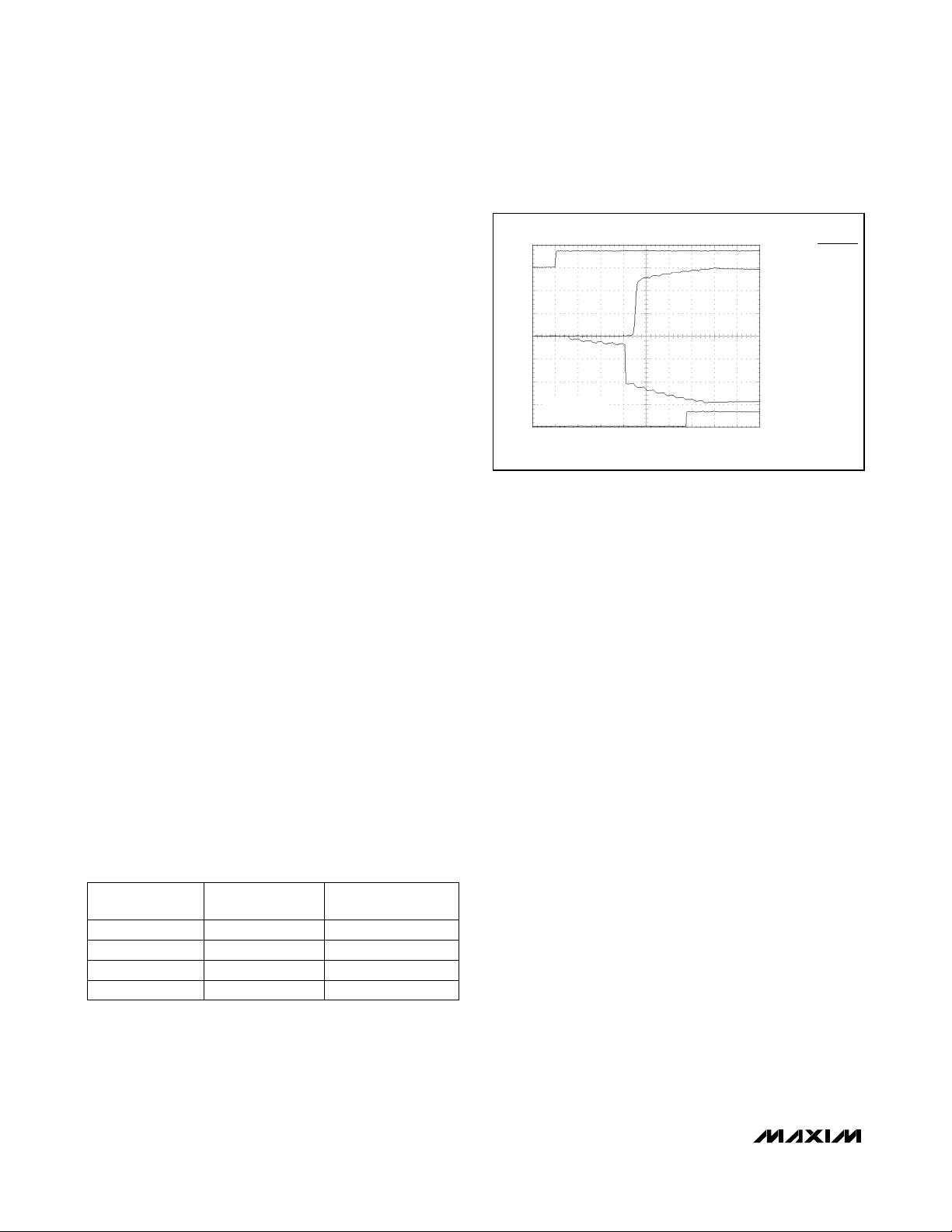
Transmitter Outputs
when Exiting Shutdown
Figure 8 shows two transmitter outputs when exiting
shutdown mode. As they become active, the two transmitter outputs are shown going to opposite RS-232 levels (one transmitter input is high, the other is low). Each
V
CC
(V)
C2, C3, C4
(
µF)
3.0 to 3.6 0.22
3.15 to 3.6 0.1
C1, C
BYPASS
(µF)
0.22
0.1
4.5 to 5.5 0.33
3.0 to 5.5 1
0.047
0.22
Table 3. Required Minimum Capacitance
Values
Figure 8. Transmitter Outputs when Exiting Shutdown or
Powering Up
5V/div
0
2V/div
0
5V/div
0
VCC = 3.3V
C1–C4 = 0.1μF
5μs/div
FORCEON = FORCEOFF
T1OUT
T2OUT
READY
Page 15
transmitter is loaded with 3kΩ in parallel with 1000pF.
The transmitter outputs display no ringing or undesirable transients as they come out of shutdown. Note that
the transmitters are enabled only when the magnitude
of V- exceeds approximately -3V.
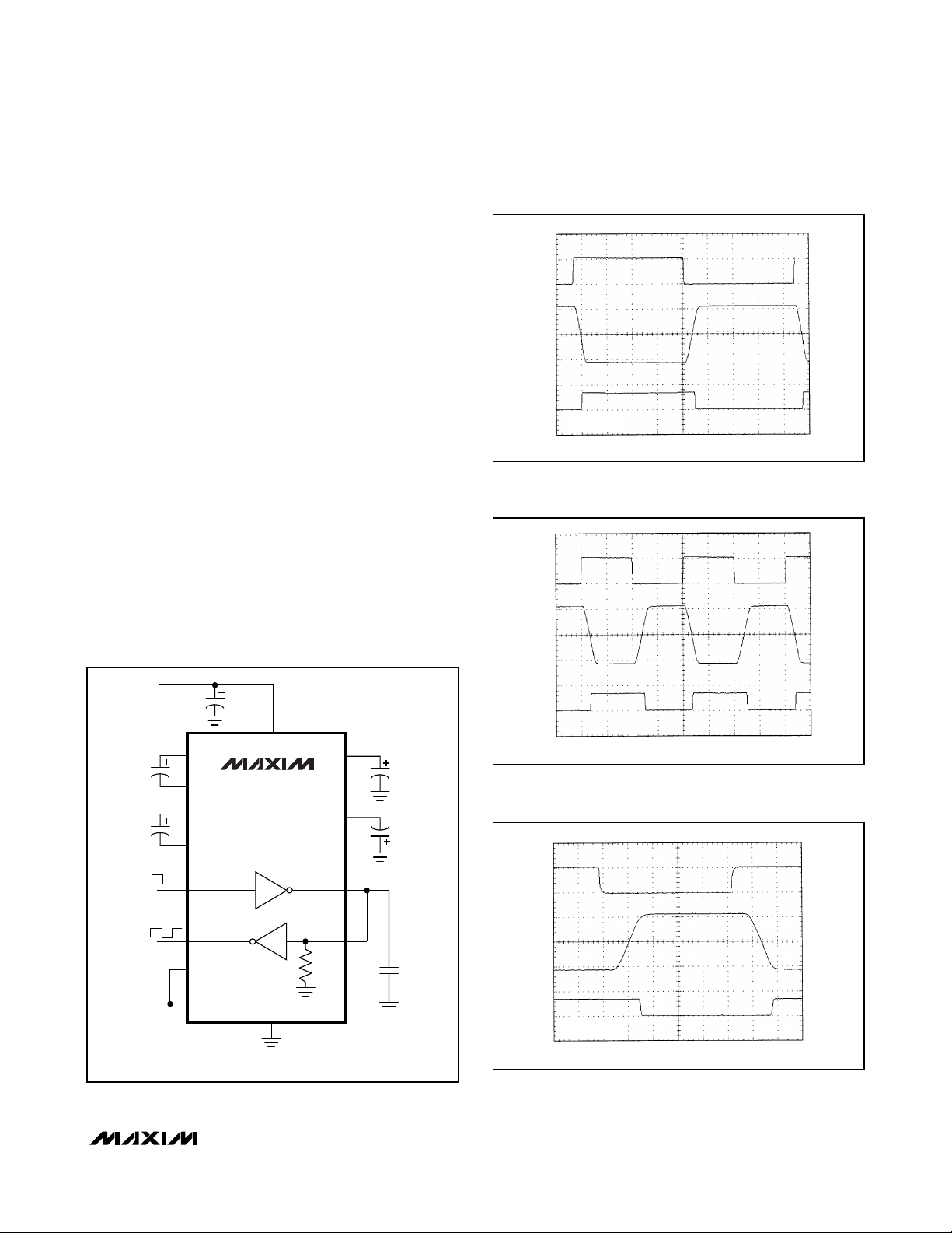
High Data Rates
The MAX3224E/MAX3226E/MAX3244E maintain the
RS-232 ±5.0V minimum transmitter output voltage even
at high data rates. Figure 9 shows a transmitter loopback test circuit. Figure 10 shows a loopback test result
at 120kbps, and Figure 11 shows the same test at
250kbps. For Figure 10, all transmitters were driven
simultaneously at 120kbps into RS-232 loads in parallel
with 1000pF. For Figure 11, a single transmitter was driven at 250kbps, and all transmitters were loaded with
an RS-232 receiver in parallel with 250pF.
The MAX3225E/MAX3227E/MAX3245E maintain the
RS-232 ±5.0V minimum transmitter output voltage at
data rates up to 1Mbps (MegaBaud). Figure 12 shows
a loopback test result with a single transmitter driven at
1Mbps and all transmitters loaded with an RS-232
receiver in parallel with 250pF.
MAX3224E–MAX3227E/MAX3244E/MAX3245E
†
±15kV ESD-Protected, 1µA, 1Mbps 3.0V to 5.5V,
RS-232 Transceivers with AutoShutdown Plus
______________________________________________________________________________________ 15
Figure 9. Loopback Test Circuit
Figure 10. MAX3224E/MAX3226E/MAX3244E Loopback Test
Result at 120kbps
Figure 11. MAX3224E/MAX3226E/MAX3244E Loopback Test
Result at 250kbps
Figure 12. MAX3225E/MAX3227E/MAX3245E Loopback Test
Result at 1Mbps
T1IN
T1OUT
R1OUT
VCC = 3.3V
2μs/div
5V/div
5V/div
5V/div
T1IN
T1OUT
5V/div
5V/div
V
CC
C
BYPASS
C1+
C1
C2
V
CC
*C3 CAN BE RETURNED TO VCC OR GND.
C1-
C2+
C2-
T_ IN
R_ OUT
FORCEON
FORCEOFF
MAX3224E
MAX3225E
MAX3226E
MAX3227E
MAX3244E
MAX3245E
GND
R1OUT
VCC = 3.3V
V
CC
V+
C3*
2μs/div
5V/div
T1IN
T1OUT
R1OUT
VCC = 3.3V
5V/div
5V/div
5V/div
200ns/div
T_ OUT
R_ IN
5kΩ
V-
C4
1000pF
Page 16

MAX3224E–MAX3227E/MAX3244E/MAX3245E
†
±15kV ESD-Protected, 1µA, 1Mbps 3.0V to 5.5V,
RS-232 Transceivers with AutoShutdown Plus
16 ______________________________________________________________________________________
Figure 13a. Mouse Driver Test Circuit
C1
0.1μF
C2
0.1μF
LOGIC
INPUTS
+3.3V
0.1μF
26
V
28
C1+
24
C1-
1
C2+
2
C2-
T1IN
14
T2IN
13
T3IN
12
R2OUTB
20
R1OUT
19
CC
MAX3244E
MAX3245E
5kΩ
V+
V-
T1OUT 9
T2OUT 10
T3OUT
R1IN
27
C3
0.1μF
3
C4
0.1μF
11
4
COMPUTER SERIAL PORT
+V
+V
-V
GND
Tx
R2OUT
18
LOGIC
OUTPUTS
R3OUT
17
R4OUT
16
R5OUT
15
23
FORCEON
V
CC
TO POWER-
MANAGEMENT
UNIT
22
21
FORCEOFF
INVALID
GND
25
5kΩ
5kΩ
5kΩ
5kΩ
R2IN 5
R3IN
R4IN
R5IN 8
6
7
RS-232
INPUTS
SERIAL
MOUSE
Page 17

MAX3224E–MAX3227E/MAX3244E/MAX3245E
†
±15kV ESD-Protected, 1µA, 1Mbps 3.0V to 5.5V,
RS-232 Transceivers with AutoShutdown Plus
______________________________________________________________________________________ 17
Mouse Driveability
The MAX3244E/MAX3245E are specifically designed to
power serial mice while operating from low-voltage
power supplies. They have been tested with leading
mouse brands from manufacturers such as Microsoft
and Logitech. The MAX3244E/MAX3245E successfully
drove all serial mice tested and met their respective
current and voltage requirements. The MAX3244E/
MAX3245E dual charge pump ensures the transmitters
supply at least ±5V during worst-case conditions.
Figure 13b shows the transmitter output voltages under
increasing load current. Figure 13a shows a typical
mouse connection.
Interconnection with 3V and 5V Logic
The MAX3224E–MAX3227E/MAX3244E/MAX3245E can
directly interface with various 5V logic families, including ACT and HCT CMOS. See Table 4 for more information on possible combinations of interconnections.
Table 5 lists other Maxim ESD-powered transceivers.
SYSTEM
POWER-SUPPLY
VOLTAGE (V)
COMPATIBILITY
3.3 Compatible with all CMOS families
5 Compatible with all TTL and CMOS families
VCCSUPPLY
VOLTAGE
(V)
3.3
5
5 Compatible with ACT and HCT CMOS, and with AC, HC, or CD4000 CMOS3.3
PART
SUPPLY
VOLTAGE
RANGE
(V)
NO.
OF
Tx/Rx
GUARANTEED
DATA RATE
(kbps)
MAX3241E +3.0 to +5.5 3/5 250
MAX3243E +3.0 to +5.5 3/5 250
MAX3244E +3.0 to +5.5 3/5 250
MAX3245E +3.0 to +5.5 3/5 1Mbps
MAX3232E +3.0 to +5.5 2/2 250
MAX3222E +3.0 to +5.5 2/2 250
MAX3223E +3.0 to +5.5 2/2 250
MAX3224E +3.0 to +5.5 2/2 250
MAX3225E +3.0 to +5.5 2/2 1Mbps
MAX3221E +3.0 to +5.5 1/1 250
MAX3227E +3.0 to +5.5 1/1 1Mbps
MAX3226E +3.0 to +5.5 1/1 250
SUPPLY
CURRENT
(
µA)
300
1
1
1
300
300
1
1
1
1
1
1
Auto-
Shutdown
Plus
—
—
Yes
Yes
—
—
—
Yes
Yes
—
Yes
Yes
Auto-
Shutdown
—
Yes
—
—
—
—
Yes
—
—
Yes
—
—
Human
Body
Model
(kV)
±15
±15
±15
±15
±15
±15
±15
±15
±15
±15
±15
±15
IEC 1000-4-2
Contact
Discharge
(kV)
±8
±8
±8
±8
±8
±8
±8
±8
±8
±8
±8
±8
IEC 1000-4-2
Air-Gap
Discharge
(kV)
±15
±15
±15
±15
±15
±15
±15
±15
±15
±15
±15
±15
Figure 13b. MAX324_E Transmitter Output Voltage vs. Load
Current per Transmitter
Table 5. ±15kV ESD-Protected, 3.0V to 5.5V Powered RS-232 Transceivers from Maxim
Table 4. Logic Family Compatibility with Various Supply Voltages
6
5
4
VCC = 3.0V
3
2
1
0
-1
-2
V
CC
-3
-4
TRANSMITTER OUTPUT VOLTAGE (V)
-5
-6
012345678910
LOAD CURRENT PER TRANSMITTER (mA)
V
V
OUT+
OUT-
V
OUT+
MAX2343E-FIG15
V
OUT-
Page 18

MAX3224E–MAX3227E/MAX3244E/MAX3245E
†
±15kV ESD-Protected, 1µA, 1Mbps 3.0V to 5.5V,
RS-232 Transceivers with AutoShutdown Plus
18 ______________________________________________________________________________________
___________________________________________________Typical Operating Circuits
+3.3V
26
V
CC
MAX3244E***
MAX3245E
V+
V-
T1OUT 9
27
3
C
BYPASS
C1
0.1μF
C2
0.1μF
+3.3V
0.1μF
15
V
2
C1+
4
C1-
5
C2+
6
C2-
11
T1IN
CC
MAX3226E*
MAX3227E
V+
V-
T1OUT 13
3
C3
0.1μF
7
C4
0.1μF
C
BYPASS
0.1μF
0.1μF
0.1μF
C2
28
C1
C1+
24
C1-
1
C2+
2
C2-
T1IN
14
C3
0.1μF
C4
0.1μF
C
BYPASS
C1
0.1μF
C2
0.1μF
TTL/CMOS
INPUTS
TTL/CMOS
OUTPUTS
+3.3V
0.1μF
12
13
12
1
2
4
5
6
R1OUT9
READY
FORCEON
C1+
C1-
C2+
C2-
T1IN
T2IN
R1OUT15
R2OUT10
AUTOSHUTDOWN
PLUS
GND
14
19
V
CC
MAX3224E**
MAX3225E
R1IN 8
5kΩ
INVALID 10
FORCEOFF
T1OUT 17
T2OUT
R1IN
5kΩ
R2IN
T2IN
13
T3IN
12
FORCEOFF
TO POWERMANAGEMENT
UNIT
16
V
CC
3
V+
V-
C3
0.1μF
7
C4
0.1μF
RS-232
OUTPUTS
8
16
RS-232
INPUTS
9
22
23
20
19
18
17
16
15
FORCEON
R2OUTB
R1OUT
R2OUT
R3OUT
R4OUT
R5OUT
AUTOSHUTDOWN
PLUS
GND
25
T2OUT 10
T3OUT
INVALID
R1IN
R2IN 5
R3IN
R4IN
R5IN 8
11
21
4
6
7
AUTOSHUTDOWN
PLUS
GND
18
14
1
READY
FORCEON
5kΩ
INVALID 11
FORCEOFF
20
TO POWERMANAGEMENT
UNIT
V
CC
*MAX3226E/MAX3227E PIN OUT REFERS TO SSOP/TSSOP PACKAGES.
**MAX3224E/MAX3225E PIN OUT REFERS TO DIP/ SSOP/TSSOP PACKAGES.
***MAX3244E/MAX3245E PIN OUT REFERS TO SO/SSOP/TSSOP PACKAGES.
Page 19

MAX3224E–MAX3227E/MAX3244E/MAX3245E
†
±15kV ESD-Protected, 1µA, 1Mbps 3.0V to 5.5V,
RS-232 Transceivers with AutoShutdown Plus
______________________________________________________________________________________ 19
___________________________________________________________ Pin Configurations
READY
C1+
V+
C1-
C2+
C2-
V-
R1IN
TOP VIEW
FORCEOFF
TOP VIEW
1
2
3
4
MAX3226E
MAX3227E
5
6
7
8
SSOP/TSSOP
GND
16
V
17
CC
18
READY
19
20
V+
16
FORCEOFF
15
V
CC
14
GND
T1OUT
13
FORCEON
12
T1IN
11
INVALID
10
9
R1OUT
R1IN
T1OUT
15 14 12 11
13
R1OUT
FORCEON
MAX3224E
MAX3225E
EXPOSED PADDLE
12
C1+
C1-
3
C2+
45
C2-
TQFN
CC
GND
V
12 11 9
10
READY
C1+
C1-
C2+
C2-
T2OUT
R2IN
T1IN
V-
FORCEON
1
2
V+
3
4
MAX3224E
5
MAX3225E
6
V-
7
8
9
10
DIP/SSOP/TSSOP
T2IN
10
INVALID
9
8
R2OUT
R2IN
7
T2OUT
6
20
19
18
17
16
15
14
13
12
11
TOP VIEW
R1IN
R2IN
R3IN
R4IN
R5IN
N.C.
T1OUT
T2OUT
T3OUT
FORCEOFF
V
CC
GND
T1OUT
R1IN
R1OUT
FORCEON
T1IN
T2IN
INVALIDR2OUT
1
2
3
4
5
6
7
8
9
T1OUT
T2OUT
T3OUT
V-
N.C.
36 35 34 33 32 31 30 29 28
EXPOSED PADDLE
10 11 12 13 14 15 16 17 18
C2+
1
C2-
2
V-
3
R1IN
4
R2IN
5
R3IN
6
R4IN
7
R5IN
8
9
10
11
T3IN
12
T2IN
13
T1IN
14
SO/SSOP/TSSOP
C2-
C2+
N.C.
C1+V+V
MAX3245E
MAX3244E
MAX3245E
CC
N.C.
27
26
25
24
23
22
21
20
19
28
27
26
25
24
23
22
21
20
19
18
17
16
15
GND
C1FORCEON
FORCEOFF
INVALID
N.C.
R2OUTB
R1OUT
R2OUT
C1+
V+
V
CC
GND
C1-
FORCEON
FORCEOFF
INVALID
R2OUTB
R1OUT
R2OUT
R3OUT
R4OUT
R5OUT
T1IN
FORCEOFF
READY
C1+
13
14
V+
15
16
MAX3226E
MAX3227E
EXPOSED PADDLE
12
C1-
C2+
3
C2- T1OUT
8
7
INVALID
R1OUT
6
R1IN
5
4
V-
N.C.
T3IN
T2IN
N.C.
T1IN
TQFN
R5OUT
R4OUT
R3OUT
N.C.
TQFN
Page 20

MAX3224E–MAX3227E/MAX3244E/MAX3245E
†
±15kV ESD-Protected, 1µA, 1Mbps 3.0V to 5.5V,
RS-232 Transceivers with AutoShutdown Plus
20 ______________________________________________________________________________________
___________________________________________Ordering Information (continued)
___________________ Chip Information
MAX3224E TRANSISTOR COUNT: 1129
MAX3225E TRANSISTOR COUNT: 1129
MAX3226E TRANSISTOR COUNT: 1129
MAX3227E TRANSISTOR COUNT: 1129
MAX3244E/MAX3245E TRANSISTOR COUNT: 1335
PROCESS: BICMOS
*EP = Exposed paddle.
PART
MAX3225ECUP
MAX3225ECTP
MAX3225ECAP
MAX3225ECPP
MAX3225EETP
MAX3225EEUP
MAX3225EEAP
MAX3225EEPP
MAX3225EAAP
MAX3226ECTE
MAX3226ECUE
MAX3226ECAE
MAX3226EEAE
MAX3226EETE -40°C to +85°C
MAX3226EEUE
MAX3226EAAE
MAX3227ECAE
MAX3227ECTE 0°C to +70°C
MAX3227ECUE 0°C to +70°C
MAX3227EEAE
TEMP
RANGE
0°C to +70°C
0°C to +70°C
0°C to +70°C
0°C to +70°C
-40°C to +85°C
-40°C to +85°C
-40°C to +85°C
-40°C to +85°C
-40°C to +125°C
0°C to +70°C
0°C to +70°C
0°C to +70°C
-40°C to +85°C
-40°C to +85°C
-40°C to +125°C
0°C to +70°C
-40°C to +85°C
PIN
PKG
20 TSSOP —
20 TQFN-
EP*
20 SSOP —
20 Plastic
DIP
20 TQFN -
EP*
20 TSSOP —
20 SSOP —
20 Plastic
DIP
20 SSOP —
16 TQFN-
EP*
16 TSSOP —
16 SSOP —
16 SSOP —
16 TQFN-
EP*
16 TSSOP —
16 SSOP —
16 SSOP —
16 TQFN-
EP*
16
TSSOP
16 SSOP —
PKG
CODE
T2055-5
—
T2055-5
—
T1655-2
T1655-2
T1655-2
—
PART
MAX3227EETE -40°C to +85°C
MAX3227EEUE -40°C to +85°C
MAX3227EAAE -40°C to +125°C 16 SSOP —
MAX3244ECWI 0°C to +70°C
MAX3244ECAI 0°C to +70°C 28 SSOP
MAX3244ECUI 0°C to +70°C
MAX3244EEWI -40°C to +85°C
MAX3244EEAI -40°C to +85°C 28 SSOP —
MAX3244EEUI -40°C to +85°C
MAX3245ECWI 0°C to +70°C
MAX3245ECAI 0°C to +70°C 28 SSOP —
MAX3245ECTX 0°C to +70°C
MAX3245EEAI -40°C to +85°C 28 SSOP —
MAX3245EEWI -40°C to +85°C
MAX3245EEUI -40°C to +85°C
MAX3245EETX -40°C to +85°C
TEMP
RANGE
PIN
PKG
16 TQFN-
EP*
16
TSSOP
28 Wide
SO
28
TSSOP
28 Wide
SO
28
TSSOP
28 Wide
SO
36 TQ FN -
E P *
28 WIDE
SO
28
TSSOP
36 TQ FN -
E P *
PKG
CODE
T1655-2
—
—
—
—
—
—
T3666-3
—
—
T3666-3
Page 21

MAX3224E–MAX3227E/MAX3244E/MAX3245E
†
±15kV ESD-Protected, 1µA, 1Mbps 3.0V to 5.5V,
RS-232 Transceivers with AutoShutdown Plus
______________________________________________________________________________________ 21
Package Information
(The package drawing(s) in this data sheet may not reflect the most current specifications. For the latest package outline information,
go to www.maxim-ic.com/packages
.)
QFN THIN.EPS
Page 22

MAX3224E–MAX3227E/MAX3244E/MAX3245E
†
±15kV ESD-Protected, 1µA, 1Mbps 3.0V to 5.5V,
RS-232 Transceivers with AutoShutdown Plus
22 ______________________________________________________________________________________
Package Information
(The package drawing(s) in this data sheet may not reflect the most current specifications. For the latest package outline information,
go to www.maxim-ic.com/packages
.)
TSSOP4.40mm.EPS
PACKAGE OUTLINE, TSSOP 4.40mm BODY
21-0066
1
I
1
Page 23

MAX3224E–MAX3227E/MAX3244E/MAX3245E
†
±15kV ESD-Protected, 1µA, 1Mbps 3.0V to 5.5V,
RS-232 Transceivers with AutoShutdown Plus
______________________________________________________________________________________ 23
Package Information
(The package drawing(s) in this data sheet may not reflect the most current specifications. For the latest package outline information,
go to www.maxim-ic.com/packages
.)
NOTES:
1. D&E DO NOT INCLUDE MOLD FLASH.
2. MOLD FLASH OR PROTRUSIONS NOT TO EXCEED .15 MM (.006").
3. CONTROLLING DIMENSION: MILLIMETERS.
4. MEETS JEDEC MO150.
5. LEADS TO BE COPLANAR WITHIN 0.10 MM.
12
INCHES
DIM
MIN
A
0.068
A1
0.002
B
0.010
C
HE
N
A
e
B
D
A1
D
E
e
H
L
0.004
0.205
0.0256 BSC
0.301
0.025
0∞
MILLIMETERS
MAX
MIN
0.078
1.73 1.99
0.008
0.05
0.25
0.015
0.09
0.008
SEE VARIATIONS
0.212
5.20
0.311
7.65
0.037
0.63
8∞
L
0.65 BSC
0∞
MAX
0.21
0.38
0.20
5.38
7.90
0.95
8∞
INCHES
MAX
MIN
D
0.239
0.249
D
0.239
0.249
D
0.278
0.289
D
0.317
0.328
0.397
0.407
D
PROPRIETARY INFORMATION
TITLE:
PACKAGE OUTLINE, SSOP, 5.3 MM
MILLIMETERS
MAX
MIN
6.07
6.33
6.07
6.33
7.33
7.07
8.33
8.07
10.33
10.07
21-0056
SSOP.EPS
N
14L
16L
20L
24L
28L
C
REV.DOCUMENT CONTROL NO.APPROVAL
1
C
1
N
1
e
TOP VIEW
D
FRONT VIEW
INCHES
MIN
DIM
0.093A
0.004
A1
0.014
B
0.009
C
H
E
A
B
A1
C
L
e 0.050 1.27
0.291
E
H 0.4190.394 10.00 10.65
0.016L
VARIATIONS:
INCHES
MINDIM
D
0.398 0.413 AA10.5010.10 16
D
0.447 0.463 AB11.7511.35 18
D 0.6140.598 15.20 2415.60 AD
D 0.7130.697 17.70 2818.10 AE
0∞-8∞
SIDE VIEW
PROPRIETARY INFORMATION
TITLE:
PACKAGE OUTLINE, .300" SOIC
MAX
0.104
0.012
0.019
0.013
0.299
0.050
MAX
0.5120.496D
MILLIMETERS
MAX
MIN
2.35
2.65
0.10
0.30
0.35
0.49
0.23
0.32
7.40 7.60
0.40 1.27
MILLIMETERS
MAX
MIN
12.60 13.00
21-0042
N MS013
20 AC
REV.DOCUMENT CONTROL NO.APPROVAL
B
1
SOICW.EPS
1
Page 24

MAX3224E–MAX3227E/MAX3244E/MAX3245E
†
±15kV ESD-Protected, 1µA, 1Mbps 3.0V to 5.5V,
RS-232 Transceivers with AutoShutdown Plus
24 ______________________________________________________________________________________
Package Information (continued)
(The package drawing(s) in this data sheet may not reflect the most current specifications. For the latest package outline information,
go to www.maxim-ic.com/packages
.)
PDIPN.EPS
Page 25

MAX3224E–MAX3227E/MAX3244E/MAX3245E
†
±15kV ESD-Protected, 1µA, 1Mbps 3.0V to 5.5V,
RS-232 Transceivers with AutoShutdown Plus
______________________________________________________________________________________ 25
Package Information (continued)
(The package drawing(s) in this data sheet may not reflect the most current specifications. For the latest package outline information,
go to www.maxim-ic.com/packages
.)
QFN THIN.EPS
Page 26

MAX3224E–MAX3227E/MAX3244E/MAX3245E
†
±15kV ESD-Protected, 1µA, 1Mbps 3.0V to 5.5V,
RS-232 Transceivers with AutoShutdown Plus
Maxim cannot assume responsibility for use of any circuitry other than circuitry entirely embodied in a Maxim product. No circuit patent licenses are
implied. Maxim reserves the right to change the circuitry and specifications without notice at any time.
26 ____________________Maxim Integrated Products, 120 San Gabriel Drive, Sunnyvale, CA 94086 408-737-7600
© 2007 Maxim Integrated Products is a registered trademark of Maxim Integrated Products, Inc.
Package Information (continued)
(The package drawing(s) in this data sheet may not reflect the most current specifications. For the latest package outline information,
go to www.maxim-ic.com/packages
.)
Revision History
Pages changed at Rev 4: 1, 12, 20, 25, 26
 Loading...