

现货库存、技术资料、百科信息、热点资讯,精彩尽在鼎好!
________________General Description
The MAX3222E/MAX3232E/MAX3237E/MAX3241E are
3V-powered EIA/TIA-232 and V.28/V.24 communications
interfaces with low power requirements, high datarate capabilities, and enhanced electrostatic discharge
(ESD) protection. All transmitter outputs and receiver
inputs are protected to ±15kV using IEC 1000-4-2 AirGap Discharge, ±8kV using IEC 1000-4-2 Contact Discharge, and ±15kV using the Human Body Model. The
MAX3237E’s logic and receiver I/O pins are protected to
the above standards, while the transmitter output pins are
protected to ±15kV using the Human Body Model.
The transceivers have a proprietary low-dropout transmitter output stage, delivering true RS-232 performance from
a +3.0V to +5.5V supply with a dual charge pump. The
charge pump requires only four small 0.1µF capacitors
for operation from a +3.3V supply. Each device is guaranteed to run at data rates of 250kbps while maintaining RS232 output levels. The MAX3237E is guaranteed to run at
data rates of 250kbps in the normal operating mode and
1Mbps in the MegaBaud™ operating mode while maintaining RS-232-compliant output levels.
The MAX3222E/MAX3232E have two receivers and two
drivers. The MAX3222E features a 1µA shutdown mode
that reduces power consumption and extends battery
life in portable systems. Its receivers can remain active
in shutdown mode, allowing external devices such as
modems to be monitored using only 1µA supply current.
Both the MAX3222E and MAX3232E are pin, package,
and functionally compatible with the industry-standard
MAX242 and MAX232, respectively.
The MAX3241E is a complete serial port (three drivers/five
receivers) designed for notebook and subnotebook computers. The MAX3237E (five drivers/three receivers) is ideal
for peripheral applications that require fast data transfer.
Both devices feature a shutdown mode in which all
receivers can remain active while using a supply current of only 1µA (MAX3241E) or 10nA (MAX3237E). The
MAX3237E/MAX3241E have additional receiver outputs
that always remain active.
The MAX3222E and MAX3232E are available in spacesaving SO, SSOP, and TSSOP packages. The MAX3241E
is available in SO and SSOP packages. The MAX3237E is
available in an SSOP package.
________________________Applications
Notebooks, Subnotebooks, Smart Phones
and Palmtop Computers
XDSL Modems
Battery-Powered Equipment Printers
Cell-Phone Data Cables Cell Phones
____________________________Features
♦ ESD Protection for RS-232 I/O Pins
(MAX3222E/MAX3232E/MAX3241E)
±15kV—Human Body Model
±8kV—IEC 1000-4-2, Contact Discharge
±15kV—IEC 1000-4-2, Air-Gap Discharge
♦ ESD Protection for All Logic and Receiver I/O
Pins (MAX3237E)
±15kV—Human Body Model
±8kV—IEC 1000-4-2, Contact Discharge
±15kV—IEC 1000-4-2, Air-Gap Discharge
♦ ESD Protection for Transmitter Output Pins
(MAX3237E)
±15kV—Human Body Model
♦ Guaranteed Data Rate
250kbps (MAX3222E/MAX3232E/MAX3241E
and MAX3237E, normal operation)
1Mbps (MAX3237E, MegaBaud operation)
♦ Latchup Free
♦ Low-Power Shutdown with Receivers Active
1µA (MAX3222E/MAX3241E)
10nA (MAX3237E)
♦ Flow-Through Pinout (MAX3237E)
♦ Guaranteed Mouse Driveability (MAX3241E)
♦ Meets EIA/TIA-232 Specifications Down to 3.0V
MAX3222E/MAX3232E/MAX3237E/MAX3241E
†
±15kV ESD-Protected, Down to 10nA, 3.0V to 5.5V,
Up to 1Mbps, True RS-232 Transceivers
________________________________________________________________ Maxim Integrated Products 1
19-1298; Rev 3a; 1/00
_______________Ordering Information
Ordering Information continued at end of data sheet.
___________________________Selector Guide
Typical Operating Circuits appear at end of data sheet.
Pin Configurations appear at end of data sheet.
†
Covered by U.S. Patent numbers 4,636,930; 4,679,134; 4,777,577; 4,797,899; 4,809,152; 4,897,774; 4,999,761; and other patents pending.
MegaBaud is a trademark of Maxim Integrated Products.
For free samples and the latest literature, visit www.maxim-ic.com or phone 1-800-998-8800.
For small orders, phone 1-800-835-8769.
PART
MAX3222E
MAX3232E
MAX3237E
(Normal)
MAX3237E
(MegaBaud)
MAX3241E 3/5
5/3
5/3
2/2
2/2
NO. OF
DRIVERS/
RECEIVERS
LOW-
POWER
SHUTDOWN
✔
—
✔
✔
✔
250
1M
250
250
250
GUARANTEED
DATA RATE
(kbps)
MAX3222ECAP
MAX3222ECUP
PART TEMP. RANGE
0°C to +70°C
0°C to +70°C 20 SSOP
20 TSSOP
PIN-PACKAGE
MAX3222E/MAX3232E/MAX3237E/MAX3241E
±15kV ESD-Protected, Down to 10nA, 3.0V to 5.5V,
Up to 1Mbps, True RS-232 Transceivers
2 _______________________________________________________________________________________
ABSOLUTE MAXIMUM RATINGS
ELECTRICAL CHARACTERISTICS
(VCC= +3.0V to +5.5V, C1–C4 = 0.1µF, TA= T
MIN
to T
MAX
, unless otherwise noted. Typical values are at TA= +25°C.) (Note 2)
Stresses beyond those listed under “Absolute Maximum Ratings” may cause permanent damage to the device. These are stress ratings only, and functional
operation of the device at these or any other conditions beyond those indicated in the operational sections of the specifications is not implied. Exposure to
absolute maximum rating conditions for extended periods may affect device reliability.
VCCto GND..............................................................-0.3V to +6V
V+ to GND (Note 1) ..................................................-0.3V to +7V
V- to GND (Note 1) ...................................................+0.3V to -7V
V+ + |V-| (Note 1) .................................................................+13V
Input Voltages
T_IN, EN, SHDN, MBAUD to GND ........................-0.3V to +6V
R_IN to GND .....................................................................±25V
Output Voltages
T_OUT to GND...............................................................±13.2V
R_OUT, R_OUTB (MAX3241E)................-0.3V to (V
CC
+ 0.3V)
Short-Circuit Duration, T_OUT to GND.......................Continuous
Continuous Power Dissipation (T
A
= +70°C)
16-Pin SSOP (derate 7.14mW/°C above +70°C) ..........571mW
16-Pin Wide SO (derate 9.52mW/°C above +70°C) .....762mW
18-Pin Wide SO (derate 9.52mW/°C above +70°C) .....762mW
18-Pin PDIP (derate 11.11mW/°C above +70°C)..........889mW
20-Pin TSSOP (derate 7.0mW/°C above +70°C) ..........559mW
20-Pin SSOP (derate 8.00mW/°C above +70°C) ..........640mW
28-Pin SSOP (derate 9.52mW/°C above +70°C) ..........762mW
28-Pin Wide SO (derate 12.50mW/°C above +70°C) .............1W
Operating Temperature Ranges
MAX32_ _EC_ _ ...................................................0°C to +70°C
MAX32_ _EE_ _.................................................-40°C to +85°C
Storage Temperature Range .............................-65°C to +150°C
Lead Temperature (soldering, 10s) .................................+300°C
Note 1: V+ and V- can have maximum magnitudes of 7V, but their absolute difference cannot exceed 13V.
VCC= 5.0V
VCC= 3.3V
VCC= 3.3V
VCC= 5.0V
SHDN = VCC, no load
T_IN, EN, SHDN
TA = +25°C
I
OUT
= 1.6mA (MAX3222E/MAX3232E/MAX3241E)
R_OUT (MAX3222E/MAX3237E/MAX3241E), EN = VCC,
receivers disabled
µA
T_IN, EN, SHDN, MBAUD
T_IN, EN, SHDN, MBAUD
I
OUT
= -1.0mA
CONDITIONS
±0.01 ±1
Input Leakage Current
SHDN = GND
µA110
Shutdown Supply Current
V
0.8 1.5
Input Threshold Low
0.6 1.1
V-25 +25Input Voltage Range
V
VCC-VCC-
0.6 0.1
Output Voltage High
mA
0.3 1
Supply Current
V
0.4
Output Voltage Low
µA±0.05 ±10Output Leakage Current
V0.5Transmitter Input Hysteresis
V0.8Input Logic Low
2.0
V
2.4
Input Logic High
UNITSMIN TYP MAXPARAMETER
MAX3222E, MAX3232E,
MAX3241E
MAX3237E 0.5 2.0
SHDN = R_IN = GND, T_IN = GND or V
CC
(MAX3237E)
nA10 300
MAX3222E, MAX3232E,
MAX3241E
T_IN, SHDN, MBAUD
918MAX3237E (Note 3)
I
OUT
= 1.0mA (MAX3237E) 0.4
DC CHARACTERISTICS (VCC= +3.3V or +5.0V, TA= +25°C)
LOGIC INPUTS
RECEIVER OUTPUTS
RECEIVER INPUTS
MAX3222E/MAX3232E/MAX3237E/MAX3241E
±15kV ESD-Protected, Down to 10nA, 3.0V to 5.5V,
Up to 1Mbps, True RS-232 Transceivers
_______________________________________________________________________________________ 3
Note 2: MAX3222E/MAX3232E/MAX3241E: C1–C4 = 0.1µF tested at 3.3V ±10%; C1 = 0.047µF, C2–C4 = 0.33µF tested at 5.0V
±10%. MAX3237E: C1–C4 = 0.1µF, tested at 3.3V ±5%; C1–C4 = 0.22µF tested at 3.3V ±10%; C1 = 0.047µF, C2–C4 =
0.33µF tested at 5.0V ±10%.
Note 3: The MAX3237E logic inputs have an active positive feedback resistor. The input current goes to zero when the inputs are at
the supply rails.
Note 4: Transmitter skew is measured at the transmitter zero crosspoints.
ELECTRICAL CHARACTERISTICS (continued)
(VCC= +3.0V to +5.5V, C1–C4 = 0.1µF, TA= T
MIN
to T
MAX
, unless otherwise noted. Typical values are at TA= +25°C.) (Note 2)
TA = +25°C
IEC 1000-4-2 Contact Discharge (except MAX3237E)
IEC 1000-4-2 Air-Gap Discharge (except MAX3237E)
Human Body Model
TA = +25°C
VCC= 0 or 3V to 5.5V, V
OUT
= ±12V, transmitters disabled
(MAX3222E/MAX3232E/MAX3241E)
T1IN = T2IN = GND, T3IN = VCC, T3OUT loaded with 3kΩ
to GND, T1OUT and T2OUT loaded with 2.5mA each
CONDITIONS
V0.5Input Hysteresis
V
1.5 2.4
Input Threshold High
±8
R_IN, T_OUT
±15
kV
±15
kΩ357Input Resistance
µA±25Output Leakage Current
V±5Transmitter Output Voltage
UNITSMIN TYP MAXPARAMETER
TIMING CHARACTERISTICS—MAX3222E/MAX3232E/MAX3241E
(VCC= +3.0V to +5.5V, C1–C4 = 0.1µF, TA= T
MIN
to T
MAX
, unless otherwise noted. Typical values are at TA= +25°C.) (Note 2)
V
CC
= 0, transmitter output = ±2V Ω300 50kOutput Resistance
TRANSMITTER OUTPUTS
mA±60Output Short-Circuit Current
2.0 2.4
All transmitter outputs loaded with 3kΩ to ground V±5 ±5.4Output Voltage Swing
VCC= 3.3V
VCC= 5.0V
MAX3237E
±8
T_IN, R_IN, R_OUT, EN, SHDN,
MBAUD
±15
kV
±15
RECEIVER INPUTS
MOUSE DRIVEABILITY (MAX3241E)
ESD PROTECTION
Human Body Model
IEC 1000-4-2 Air-Gap Discharge
IEC 1000-4-2 Contact Discharge
Transition-Region Slew Rate
430
V/µs
CL= 150pF to
2500pF
CL= 150pF to
1000pF
PARAMETER SYMBOL MIN TYP MAX UNITS
Receiver Skew
t
PHL
- t
PLH
50 ns
Transmitter Skew
t
PHL
- t
PLH
100 ns
Receiver Output Disable Time 200 ns
Receiver Output Enable Time 200 ns
630
Maximum Data Rate 250 kbps
t
PHL
0.15
Receiver Propagation Delay
t
PLH
0.15
µs
CONDITIONS
(Note 4)
Normal operation (except MAX3232E)
Normal operation (except MAX3232E)
VCC= 3.3V,
TA= +25°C,
RL= 3kΩ to 7kΩ,
measured from +3V
to -3V or -3V to +3V
RL= 3kΩ, CL= 1000pF,
one transmitter switching
Receiver input to receiver output,
C
L
= 150pF
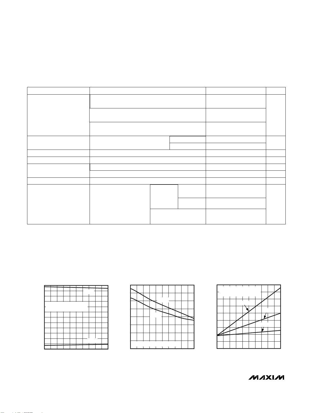
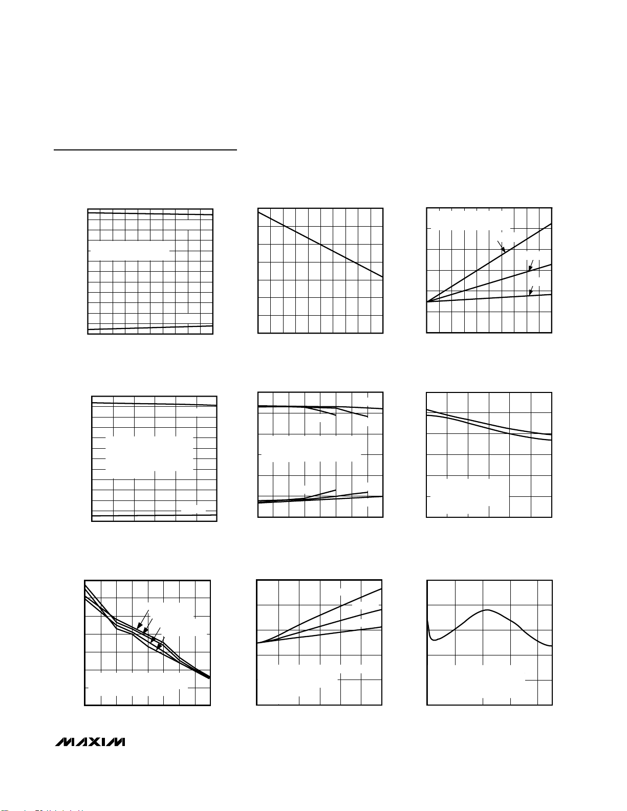
__________________________________________Typical Operating Characteristics
(VCC= +3.3V, 250kbps data rate, 0.1µF capacitors, all transmitters loaded with 3kΩ and CL, TA = +25°C, unless otherwise noted.)
-6
-5
-4
-3
-2
-1
0
1
2
3
4
5
6
0 1000 2000 3000 4000 5000
MAX3222E/MAX3232E
TRANSMITTER OUTPUT VOLTAGE
vs. LOAD CAPACITANCE
MAX3237E toc01
LOAD CAPACITANCE (pF)
TRANSMITTER OUTPUT VOLTAGE (V)
T1 TRANSMITTING AT 250kbps
T2 TRANSMITTING AT 15.6kbps
V
OUT+
V
OUT-
0
6
2
4
10
8
14
12
16
0 1000 2000 3000 4000 5000
MAX3222E/MAX3232E
SLEW RATE vs. LOAD CAPACITANCE
MAX3237E toc02
LOAD CAPACITANCE (pF)
SLEW RATE (V/µs)
+SLEW
FOR DATA RATES UP TO 250kbps
-SLEW
0
25
20
15
5
10
35
30
40
45
0 20001000 3000 4000 5000
MAX3222E/MAX3232E
OPERATING SUPPLY CURRENT
vs. LOAD CAPACITANCE
MAX3237E toc03
LOAD CAPACITANCE (pF)
SUPPLY CURRENT (mA)
250kbps
120kbps
20kbps
T1 TRANSMITTING AT 250kbps
T2 TRANSMITTING AT 15.6kbps
MAX3222E/MAX3232E/MAX3237E/MAX3241E
±15kV ESD-Protected, Down to 10nA, 3.0V to 5.5V,
Up to 1Mbps, True RS-232 Transceivers
4 _______________________________________________________________________________________
TIMING CHARACTERISTICS—MAX3237E
(VCC= +3.0V to +5.5V, C1–C4 = 0.1µF, TA= T
MIN
to T
MAX
, unless otherwise noted. Typical values are at TA= +25°C.) (Note 2)
24 150
MBAUD =
V
CC
Transition-Region Slew Rate
VCC= 3.3V, RL= 3kΩ to
7kΩ, +3V to -3V or -3V to
+3V, TA= +25°C
MBAUD =
GND
CL= 150pF
to 1000pF
t
PLH
t
PHL
V/µs
630
Receiver Skew 50 ns
|
t
PHL
- t
PLH
|
Transmitter Skew
100 ns
| t
PHL
- t
PLH
|, MBAUD = V
CC
R_IN to R_OUT, CL= 150pF
Maximum Data Rate
1000
kbps
VCC= 4.5V to 5.5V, RL= 3kΩ, CL= 1000pF,
one transmitter switching, MBAUD = V
CC
1000
VCC= 3.0V to 4.5V, RL= 3kΩ, CL= 250pF,
one transmitter switching, MBAUD = V
CC
PARAMETER MIN TYP MAX UNITS
Receiver Output Enable Time 2.6 µs
Receiver Propagation Delay
0.15
µs
250
0.15
100 ns
| t
PHL
- t
PLH
|, MBAUD = GND
Receiver Output Disable Time 2.4 µsNormal operation
CONDITIONS
Normal operation
RL= 3kΩ, CL= 1000pF, one transmitter switching,
MBAUD = GND
430
CL= 150pF to 2500pF,
MBAUD = GND
MAX3222E/MAX3232E/MAX3237E/MAX3241E
±15kV ESD-Protected, Down to 10nA, 3.0V to 5.5V,
Up to 1Mbps, True RS-232 Transceivers
_______________________________________________________________________________________ 5
MAX3238E toc01
Typical Operating Characteristics (continued)
(VCC= +3.3V, 250kbps data rate, 0.1µF capacitors, all transmitters loaded with 3kΩ and CL, TA = +25°C, unless otherwise noted.)
-6
-5
-4
-3
-2
-1
0
1
2
3
4
5
6
0 1000 2000 3000 4000 5000
MAX3241E
TRANSMITTER OUTPUT VOLTAGE
vs. LOAD CAPACITANCE
MAX3237E to04
LOAD CAPACITANCE (pF)
TRANSMITTER OUTPUT VOLTAGE (V)
1 TRANSMITTER AT 250kbps
2 TRANSMITTERS AT 15.6kbps
V
OUT+
V
OUT-
0
30
20
10
40
50
60
0 20001000 3000 4000 5000
MAX3241E
OPERATING SUPPLY CURRENT
vs. LOAD CAPACITANCE
MAX3237E toc06
LOAD CAPACITANCE (pF)
SUPPLY CURRENT (mA)
250kbps
120kbps
20kbps
1 TRANSMITTER AT 250kbps
2 TRANSMITTERS AT 15.6kbps
0
4
2
8
6
12
10
14
0 1000 2000 3000 4000 5000
MAX3241E
SLEW RATE vs. LOAD CAPACITANCE
MAX3237E toc05
LOAD CAPACITANCE (pF)
SLEW RATE (V/µs)
TRANSMITTER OUTPUT VOLTAGE
vs. LOAD CAPACITANCE
6
5
4
3
2
FOR DATA RATES UP TO 250kbps
1
1 TRANSMITTER 250kbps
4 TRANSMITTERS 15.6kbps
0
ALL TRANSMITTERS LOADED
-1
WITH 3kΩ + C
-2
-3
-4
TRANSMITTER OUTPUT VOLTAGE (V)
-5
-6
0 1000 1500500 2000 2500 300
SLEW RATE vs. LOAD CAPACITANCE
70
60
50
40
30
SLEW RATE (V/µs)
20
1 TRANSMITTER AT FULL DATA RATE
4 TRANSMITTERS AT 1/16 DATA RATE
10
3kΩ + C
LOAD EACH OUTPUT
L
0
0
500 1000 1500 2000
LOAD CAPACITANCE (pF)
MAX3237E
SLEW RATE vs. LOAD CAPACITANCE
12
10
8
6
SLEW RATE (V/µs)
4
1 TRANSMITTER AT 250kbps
4 TRANSMITTERS 15.6kbps
2
ALL TRANSMITTERS LOADED
WITH 3kΩ + C
0
0
TRANSMITTER SKEW vs. LOAD CAPACITANCE
100
80
60
40
|t
- t
PLH
TRANSMITTER SKEW (ns)
1 TRANSMITTER AT 500kbps
20
4 TRANSMITTERS AT 1/16 DATA RATE
ALL TRANSMITTERS LOADED
WITH 3kΩ + C
0
0
L
LOAD CAPACITANCE (pF)
MAX3237E
(MBAUD = V
CC
-SLEW, 1Mbps
+SLEW, 1Mbps
-SLEW, 2Mbps
+SLEW, 2Mbps
)
TRANSMITTER OUTPUT VOLTAGE
1Mbps
1.5Mbps
1.5Mbps
1Mbps
CC
)
MAX3237E toc08
vs. LOAD CAPACITANCE (MBAUD = V
7.5
V
+
OUT
V
OUT-
5.0
2.5
1 TRANSMITTER AT FULL DATA RATE
4 TRANSMITTERS AT 1/16 DATA RATE
0
3kΩ + C
-2.5
-5.0
TRANSMITTER OUTPUT VOLTAGE (V)
-7.5
0
2Mbps
LOAD, EACH OUTPUT
L
2Mbps
500 1000 1500 2000
LOAD CAPACITANCE (pF)
MAX3237E
SUPPLY CURRENT vs. LOAD CAPACITANCE
WHEN TRANSMITTING DATA (MBAUD = GND)
50
MAX3237E toc10
40
30
20
SUPPLY CURRENT (mA)
10
0
250kbps
120kbps
20kbps
1 TRANSMITTER AT 20kbps, 120kbps, 250kbps
4 TRANSMITTERS AT 15.6kbps
ALL TRANSMITTERS LOADED
WITH 3kΩ + C
0
L
1000 1500500 2000 2500 3000
LOAD CAPACITANCE (pF)
MAX3237E toc11
MAX3237E
(MBAUD = GND)
SR-
SR+
L
1000 1500500 2000 2500 3000
LOAD CAPACITANCE (pF)
MAX3237E
(MBAUD = V
|
PHL
L
1000 1500500 2000
LOAD CAPACITANCE (pF)
)
CC
MAX3237E toc09
MAX3237E toc12
______________________________________________________________Pin Description
MAX3222E/MAX3232E/MAX3237E/MAX3241E
±15kV ESD-Protected, Down to 10nA, 3.0V to 5.5V,
Up to 1Mbps, True RS-232 Transceivers
6 _______________________________________________________________________________________
Typical Operating Characteristics (continued)
(VCC= +3.3V, 250kbps data rate, 0.1µF capacitors, all transmitters loaded with 3kΩ and CL, TA = +25°C, unless otherwise noted.)
-6
-2
-4
2
0
4
6
-3
-5
1
-1
3
5
2.0 3.0 3.52.5 4.0 4.5 5.0
MAX3237E toc13
SUPPLY VOLTAGE (V)
TRANSMITTER OUTPUT VOLTAGE (V)
V
OUT-
V
OUT
+
1 TRANSMITTER 250kbps
4 TRANSMITTERS 15.6kbps
ALL TRANSMITTERS LOADED
WITH 3kΩ +1000pF
MAX3237E
TRANSMITTER OUTPUT VOLTAGE vs.
SUPPLY VOLTAGE (MBAUD = GND)
0
10
20
30
40
50
2.0
MAX3237E
SUPPLY CURRENT vs.
SUPPLY VOLTAGE (MBAUD = GND)
MAX3237E toc14
SUPPLY VOLTAGE (V)
SUPPLY CURRENT (mA)
3.0 3.52.5 4.0 4.5 5.0
1 TRANSMITTER AT 250kbps
4 TRANSMITTERS AT 15.6kbps
ALL TRANSMITTERS LOADED
WITH 3kΩ AND 1000pF
-5.5V Generated by the Charge PumpV-4
RS-232 Transmitter OutputsT_OUT
5, 6, 7,
10, 12
RS-232 Receiver InputsR_IN8, 9, 11
TTL/CMOS Receiver OutputsR_OUT18, 20, 21
+5.5V Generated by the Charge PumpV+27
Negative Terminal of Voltage-Doubler
Charge-Pump Capacitor
C1-25
Positive Terminal of Inverting ChargePump Capacitor
C2+1
Negative Terminal of Inverting
Charge-Pump Capacitor
C2-3
Positive Terminal of Voltage-Doubler
Charge-Pump Capacitor
C1+28
Receiver Enable. Active low.
EN
13*
FUNCTIONNAME
MAX3237E
TTL/CMOS Transmitter InputsT_IN
17*, 19*, 22*,
23*, 24*
GroundGND2
77
8, 178, 15
9, 169, 14
10, 1510, 13
12, 1311, 12
33
44
55
66
22
11
TSSOP/
SSOP
SO/DIP
MAX3222E
1816
76
8, 177, 14
9, 168, 13
12, 159, 12
13, 1410, 11
32
43
54
65
21
——
TSSOP/
SSOP
SO/DIP
MAX3232E
1815
3
9, 10, 11
4–8
15–19
12, 13, 14
27
24
1
2
28
23
PIN
MAX3241E
25

_______________Detailed Description
Dual Charge-Pump Voltage Converter
The MAX3222E/MAX3232E/MAX3237E/MAX3241E’s
internal power supply consists of a regulated dual
charge pump that provides output voltages of +5.5V
(doubling charge pump) and -5.5V (inverting charge
pump), over the 3.0V to 5.5V VCCrange. The charge
pump operates in discontinuous mode; if the output
voltages are less than 5.5V, the charge pump is
enabled, and if the output voltages exceed 5.5V, the
charge pump is disabled. Each charge pump requires
a flying capacitor (C1, C2) and a reservoir capacitor
(C3, C4) to generate the V+ and V- supplies (Figure 1).
RS-232 Transmitters
The transmitters are inverting level translators that convert TTL/CMOS-logic levels to ±5.0V EIA/TIA-232-compliant levels.
The MAX3222E/MAX3232E/MAX3237E/MAX3241E
transmitters guarantee a 250kbps data rate with worstcase loads of 3kΩ in parallel with 1000pF, providing
compatibility with PC-to-PC communication software
(such as LapLink™). Transmitters can be paralleled to
drive multiple receivers or mice.
The MAX3222E/MAX3237E/MAX3241E’s transmitters are
disabled and the outputs are forced into a high-imped-
ance state when the device is in shutdown mode (SHDN =
GND). The MAX3222E/MAX3232E/MAX3237E/MAX3241E
permit the outputs to be driven up to ±12V in shutdown.
The MAX3222E/MAX3232E/MAX3241E transmitter
inputs do not have pull-up resistors. Connect unused
inputs to GND or VCC. The MAX3237E transmitter
inputs have a 400kΩ active positive feedback resistor,
allowing unused inputs to be left unconnected.
MAX3237E MegaBaud Operation
For higher-speed serial communications, the MAX3237E
features MegaBaud operation. In MegaBaud operating
mode (MBAUD = VCC), the MAX3237E transmitters
guarantee a 1Mbps data rate with worst-case loads of
3kΩ in parallel with 250pF for 3.0V < VCC< 4.5V. For 5V
±10% operation, the MAX3237E transmitters guarantee a
1Mbps data rate into worst-case loads of 3kΩ in parallel
with 1000pF.
RS-232 Receivers
The receivers convert RS-232 signals to CMOS-logic
output levels. The MAX3222E/MAX3237E/MAX3241E
receivers have inverting three-state outputs. Drive EN
high to place the receiver(s) into a high-impedance
state. Receivers can be either active or inactive in shutdown (Table 1).
MAX3222E/MAX3232E/MAX3237E/MAX3241E
±15kV ESD-Protected, Down to 10nA, 3.0V to 5.5V,
Up to 1Mbps, True RS-232 Transceivers
_______________________________________________________________________________________ 7
_________________________________________________Pin Description (continued)
No ConnectionN.C.—
MegaBaud Control Input. Connect to
GND for normal operation; connect to
V
CC
for 1Mbps transmission rates.
MBAUD15*
Noninverting Complementary
Receiver Outputs. Always active.
R_OUTB16
Shutdown Control. Active low.
SHDN
14*
+3.0V to +5.5V Supply VoltageV
CC
26
FUNCTIONNAME
MAX3237E
11, 14—
——
——
2018
1917
TSSOP/
SSOP
SO/DIP
MAX3222E
1, 10, 11,
20
—
——
——
——
1916
TSSOP/
SSOP
SO/DIP
MAX3232E
—
—
20, 21
22
26
PIN
MAX3241E
*These pins have an active positive feedback resistor internal to the MAX3237E, allowing unused inputs to be left unconnected.
LapLink is a trademark of Traveling Software.

MAX3222E/MAX3232E/MAX3237E/MAX3241E
±15kV ESD-Protected, Down to 10nA, 3.0V to 5.5V,
Up to 1Mbps, True RS-232 Transceivers
The complementary outputs on the MAX3237E/MAX3241E
(R_OUTB) are always active, regardless of the state of EN
or SHDN. This allows the device to be used for ring indica-
tor applications without forward biasing other devices connected to the receiver outputs. This is ideal for systems
where VCCdrops to 0 in shutdown to accommodate
peripherals such as UARTs (Figure 2).
MAX3222E/MAX3237E/MAX3241E
Shutdown Mode
Supply current falls to less than 1µA in shutdown mode
(SHDN = low). The MAX3237E’s supply current falls to
10nA (typ) when all receiver inputs are in the invalid
range (-0.3V < R_IN < +0.3). When shut down, the
device’s charge pumps are shut off, V+ is pulled down
to V
CC
, V- is pulled to ground, and the transmitter
outputs are disabled (high impedance). The time
required to recover from shutdown is typically 100µs,
as shown in Figure 3. Connect SHDN to VCCif the shut-
down mode is not used. SHDN has no effect on R_OUT
or R_OUTB (MAX3237E/MAX3241E).
±15kV ESD Protection
As with all Maxim devices, ESD-protection structures
are incorporated to protect against electrostatic
discharges encountered during handling and assembly. The driver outputs and receiver inputs of the
Table 1. MAX3222E/MAX3237E/MAX3241E
Shutdown and Enable Control Truth Table
0 Active0
1 High-Z0
EN
R_OUT
SHDN
Active
High-Z
Active
1 0
Active
1 1
R_OUTB
(MAX3237E/
MAX3241E)
Active
Active
High-Z
High-Z
T_OUT
Active
Active
8 ______________________________________________________________________________________
Figure 1. Slew-Rate Test Circuits
C1
C2
V
CC
0.1µF
V
C1+
C1-
C2+
C2-
T_ IN
R_ OUT
CC
MAX3222E
MAX3232E
MAX3237E
MAX3241E
5k
GND
V
CC
0.1µF
V
C1+
C1
C2
C1-
C2+
C2-
T_ IN
R_ OUT
MINIMUM SLEW-RATE TEST CIRCUIT MAXIMUM SLEW-RATE TEST CIRCUIT
CC
MAX3222E
MAX3232E
MAX3237E
MAX3241E
GND
V+
C3
V-
C4
T_ OUT
R_ IN
5k
3k
2500pF
V+
T_ OUT
R_ IN
C3
V-
C4
7k
150pF

MAX3222E/MAX3232E/MAX3237E/MAX3241E
±15kV ESD-Protected, Down to 10nA, 3.0V to 5.5V,
Up to 1Mbps, True RS-232 Transceivers
_______________________________________________________________________________________ 9
MAX3222E/MAX3232E/MAX3237E/MAX3241E have
extra protection against static electricity. Maxim’s engineers have developed state-of-the-art structures to protect these pins against ESD of ±15kV without damage.
The ESD structures withstand high ESD in all states:
normal operation, shutdown, and powered down. After
an ESD event, Maxim’s E versions keep working without
latchup, whereas competing RS-232 products can
latch and must be powered down to remove latchup.
Furthermore, the MAX3237E logic I/O pins also have
±15kV ESD protection. Protecting the logic I/O pins to
±15kV makes the MAX3237E ideal for data cable applications.
ESD protection can be tested in various ways; the
transmitter outputs and receiver inputs for the
MAX3222E/MAX3232E/MAX3241E are characterized
for protection to the following limits:
• ±15kV using the Human Body Model
• ±8kV using the Contact Discharge method specified
in IEC 1000-4-2
• ±15kV using IEC 1000-4-2’s Air-Gap Discharge
method
For the MAX3237E, all logic and RS-232 I/O pins are
characterized for protection to ±15kV per the Human
Body Model.
ESD Test Conditions
ESD performance depends on a variety of conditions.
Contact Maxim for a reliability report that documents
test setup, test methodology, and test results.
Human Body Model
Figure 4a shows the Human Body Model, and Figure
4b shows the current waveform it generates when discharged into a low impedance. This model consists of
a 100pF capacitor charged to the ESD voltage of interest, which is then discharged into the test device
through a 1.5kΩ resistor.
Figure 2. Detection of RS-232 Activity when the UART and
Interface are Shut Down; Comparison of MAX3237E/
MAX3241E (b) with Previous Transceivers (a)
Figure 3. Transmitter Outputs Recovering from Shutdown or
Powering Up
V
CC
V
CC
PROTECTION
DIODE
Rx
UART
Tx
GND
a) OLDER RS-232: POWERED-DOWN UART DRAWS CURRENT FROM
ACTIVE RECEIVER OUTPUT IN SHUTDOWN.
TO
µP
V
CC
PROTECTION
DIODE
UART
GND
LOGIC
TRANSITION
DETECTOR
Rx
Tx
SHDN = GND
V
CC
R1OUTB
R1OUT
THREE-STATED
EN = V
T1IN
SHDN = GND
CC
PREVIOUS
RS-232
5k
MAX3237E/MAX3241E
R1IN
5k
T1OUT
5V/div
0
2V/div
0
SHDN
T2OUT
b) NEW MAX3237E/MAX3241E: EN SHUTS DOWN RECEIVER OUTPUTS
(EXCEPT FOR B OUTPUTS), SO NO CURRENT FLOWS TO UART IN SHUTDOWN.
B OUTPUTS INDICATE RECEIVER ACTIVITY DURING SHUTDOWN WITH EN HIGH.
VCC = 3.3V
C1–C4 = 0.1µF
40µs/div
T1OUT

MAX3222E/MAX3232E/MAX3237E/MAX3241E
±15kV ESD-Protected, Down to 10nA, 3.0V to 5.5V,
Up to 1Mbps, True RS-232 Transceivers
10 ______________________________________________________________________________________
IEC 1000-4-2
The IEC 1000-4-2 standard covers ESD testing and performance of finished equipment; it does not specifically
refer to integrated circuits. The MAX3222E/MAX3232E/
MAX3237E/MAX3241E help you design equipment that
meets Level 4 (the highest level) of IEC 1000-4-2, without
the need for additional ESD-protection components.
The major difference between tests done using the
Human Body Model and IEC 1000-4-2 is higher peak
current in IEC 1000-4-2 because series resistance is
lower in the IEC 1000-4-2 model. Hence, the ESD withstand voltage measured to IEC 1000-4-2 is generally
lower than that measured using the Human Body
Model. Figure 5a shows the IEC 1000-4-2 model, and
Figure 5b shows the current waveform for the ±8kV IEC
1000-4-2 Level 4 ESD Contact Discharge test.
The Air-Gap Discharge test involves approaching the
device with a charged probe. The Contact Discharge
method connects the probe to the device before the
probe is energized.
Machine Model
The Machine Model for ESD tests all pins using a
200pF storage capacitor and zero discharge resistance. Its objective is to emulate the stress caused by
contact that occurs with handling and assembly during
manufacturing. All pins require this protection during
manufacturing, not just RS-232 inputs and outputs.
Therefore, after PC board assembly, the Machine
Model is less relevant to I/O ports.
Figure 4a. Human Body ESD Test Model
Figure 4b. Human Body Model Current Waveform
Figure 5a. IEC 1000-4-2 ESD Test Model
Figure 5b. IEC 1000-4-2 ESD Generator Current Waveform
HIGH-
VOLTAGE
DC
SOURCE
R
C
1MΩ
CHARGE-CURRENT
LIMIT RESISTOR
C
100pF
s
R
D
1500Ω
DISCHARGE
RESISTANCE
STORAGE
CAPACITOR
DEVICE
UNDER
TEST
PEAK-TO-PEAK RINGING
I
r
(NOT DRAWN TO SCALE)
AMPERES
IP 100%
90%
36.8%
10%
0
0
t
RL
TIME
t
DL
CURRENT WAVEFORM
R
C
50MΩ to 100MΩ
CHARGE-CURRENT
LIMIT RESISTOR
HIGH-
VOLTAGE
DC
SOURCE
150pF
C
s
RD
330Ω
DISCHARGE
RESISTANCE
STORAGE
CAPACITOR
DEVICE
UNDER
TEST
I
100%
90%
PEAK
I
10%
tr = 0.7ns to 1ns
30ns
60ns
t

MAX3222E/MAX3232E/MAX3237E/MAX3241E
±15kV ESD-Protected, Down to 10nA, 3.0V to 5.5V,
Up to 1Mbps, True RS-232 Transceivers
______________________________________________________________________________________ 11
___________Applications Information
Capacitor Selection
The capacitor type used for C1–C4 is not critical for
proper operation; polarized or nonpolarized capacitors
can be used. The charge pump requires 0.1µF capacitors for 3.3V operation. For other supply voltages, see
Table 2 for required capacitor values. Do not use values smaller than those listed in Table 2. Increasing the
capacitor values (e.g., by a factor of 2) reduces ripple
on the transmitter outputs and slightly reduces power
consumption. C2, C3, and C4 can be increased without
changing C1’s value. However, do not increase C1
without also increasing the values of C2, C3, C4,
and C
BYPASS
to maintain the proper ratios (C1 to
the other capacitors).
When using the minimum required capacitor values,
make sure the capacitor value does not degrade
excessively with temperature. If in doubt, use capacitors with a larger nominal value. The capacitor’s equivalent series resistance (ESR), which usually rises at low
temperatures, influences the amount of ripple on V+
and V-.
Power-Supply Decoupling
In most circumstances, a 0.1µF VCCbypass capacitor
is adequate. In applications that are sensitive to powersupply noise, use a capacitor of the same value as
charge-pump capacitor C1. Connect bypass capacitors as close to the IC as possible.
Operation Down to 2.7V
Transmitter outputs will meet EIA/TIA-562 levels of
±3.7V with supply voltages as low as 2.7V.
Transmitter Outputs when
Recovering from Shutdown
Figure 3 shows two transmitter outputs when recovering from shutdown mode. As they become active, the
two transmitter outputs are shown going to opposite
RS-232 levels (one transmitter input is high, the other is
low). Each transmitter is loaded with 3kΩ in parallel with
2500pF. The transmitter outputs display no ringing or
undesirable transients as they come out of shutdown.
Note that the transmitters are enabled only when the
magnitude of V- exceeds approximately -3V.
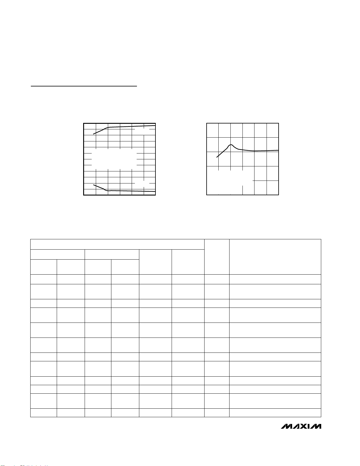
Mouse Driveability
The MAX3241E has been specifically designed to
power serial mice while operating from low-voltage
power supplies. It has been tested with leading mouse
brands from manufacturers such as Microsoft and
Logitech. The MAX3241E successfully drove all serial
mice tested and met their respective current and voltage requirements. Figure 6a shows the transmitter output voltages under increasing load current at 3.0V.
Figure 6b shows a typical mouse connection using the
MAX3241E.
High Data Rates
The MAX3222E/MAX3232E/MAX3237E/MAX3241E
maintain the RS-232 ±5.0V minimum transmitter output
voltage even at high data rates. Figure 7 shows a transmitter loopback test circuit. Figure 8 shows a loopback
test result at 120kbps, and Figure 9 shows the same test
at 250kbps. For Figure 8, all transmitters were driven
simultaneously at 120kbps into RS-232 loads in parallel
with 1000pF. For Figure 9, a single transmitter was driven at 250kbps, and all transmitters were loaded with an
RS-232 receiver in parallel with 1000pF.
Table 2. Required Minimum Capacitor
Values
0.047
C1
(µF)
0.1
0.33
C2, C3, C4
(µF)
0.47
MAX3222E/MAX3232E/MAX3241E
4.5 to 5.5
V
CC
(V)
3.0 to 5.5
Figure 6a. MAX3241E Transmitter Output Voltage vs. Load
Current per Transmitter
0.1
0.13.0 to 3.6
0.22 0.223.0 to 3.6
0.1
0.047
0.1
0.33
MAX3237E
3.15 to 3.6
4.5 to 5.5
0.22 1.03.0 to 5.5
6
5
4
VCC = 3.0V
3
2
1
0
-1
-2
V
CC
-3
-4
TRANSMITTER OUTPUT VOLTAGE (V)
-5
-6
012345678910
LOAD CURRENT PER TRANSMITTER (mA)
V
V
OUT+
OUT-
V
OUT+
V
MAX3222E-fig06a
OUT-

MAX3222E/MAX3232E/MAX3237E/MAX3241E
±15kV ESD-Protected, Down to 10nA, 3.0V to 5.5V,
Up to 1Mbps, True RS-232 Transceivers
12 ______________________________________________________________________________________
The MAX3237E maintains the RS-232 ±5.0V minimum
transmitter output voltage at data rates up to 1Mbps.
Figure 10 shows a loopback test result at 1Mbps with
MBAUD = VCC. For Figure 10, all transmitters were
loaded with an RS-232 receiver in parallel with 250pF.
Interconnection with 3V and 5V Logic
The MAX3222E/MAX3232E/MAX3237E/MAX3241E can
directly interface with various 5V logic families, including ACT and HCT CMOS. See Table 3 for more information on possible combinations of interconnections.
Figure 6b. Mouse Driver Test Circuit
V
= 3V
CC
to 5.5V
28
24
1
C2
2
14
13
12
V
CC
21
20
19
C1+
C1-
C2+
C2T1IN
T2IN
T3IN
R1OUTB
R2OUTB
R1OUT
C
BYPASS
MAX3241E
26
V
CC
T1OUT
T2OUT
T3OUT
R1IN 4
27
V+
V-
C3 C1
3
C4
9
10
11
COMPUTER SERIAL PORT
+V
+V
-V
GND
Tx
GND
5k
R2IN 5
5k
5k
5k
5k
25
R3IN
R4IN
R5IN 8
SHDN
6
7
MOUSE
22
V
CC
18
R2OUT
R3OUT
17
16
R4OUT
15
R5OUT
23
EN

MAX3222E/MAX3232E/MAX3237E/MAX3241E
±15kV ESD-Protected, Down to 10nA, 3.0V to 5.5V,
Up to 1Mbps, True RS-232 Transceivers
______________________________________________________________________________________ 13
Figure 7. Loopback Test Circuit
Figure 8. MAX3241E Loopback Test Result at 120kbps
Figure 9. MAX3241E Loopback Test Result at 250kbps
Figure 10. MAX3237E Loopback Test Result at 1000kbps
(MBAUD = V
CC
)
5
SYSTEM
POWER-SUPPLY
VOLTAGE
(V)
5
3.3
Compatible with ACT
and HCT CMOS, and
with AC, HC, or
CD4000 CMOS
COMPATIBILITY
Compatible with all
TTL and CMOS families
Compatible with all
CMOS families
3.3
VCCSUPPLY
VOLTAGE
(V)
5
3.3
Table 3. Logic-Family Compatibility with
Various Supply Voltages
V
CC
C1
C2
0.1µF
C1+
C1-
C2+
C2-
T_ IN
V
CC
MAX3222E
MAX3232E
MAX3237E
MAX3241E
V+
C3
V-
C4
T_ OUT
T1IN
T1OUT
R1OUT
VCC = 3.3V
C1–C4 = 0.1µF
2µs/div
T1IN
T1OUT
R1OUT
VCC = 3.3V, C1–C4 = 0.1µF
2µs/div
5V/div
5V/div
5V/div
5V/div
5V/div
5V/div
R_ OUT
GND
5k
R_ IN
1000pF
+5V
+5V
-5V
+5V
0
0
VCC = 3.3V
C1–C4 = 0.1µF
0
400ns/div
T_IN
T_OUT
5kΩ + 250pF
R_OUT

MAX3222E/MAX3232E/MAX3237E/MAX3241E
±15kV ESD-Protected, Down to 10nA, 3.0V to 5.5V,
Up to 1Mbps, True RS-232 Transceivers
14 ______________________________________________________________________________________
Pin Configurations
TOP VIEW
1
N.C.
C1+
C1-
C2+
C2-
T2OUT
R2IN
N.C.
C2+
C2-
R1IN
R2IN
R3IN
R4IN
R5IN
T1OUT
T2OUT
T3OUT
T3IN
T2IN
T1IN
20
2
V+
3
4
MAX3232E
5
6
V-
7
8
9
10
19
18
17
16
15
14
13
12
11
TSSOP
1
2
V-
3
4
5
MAX3241E
6
7
8
9
10
11
12
13
14
28
27
26
25
24
23
22
21
20
19
18
17
16
15
C1+
C1-
C2+
C2-
T2OUT
C1+
C1-
C2-
T2OUT
EN
1
2
V+
3
4
5
6
V-
7
8
9
1
2
V+
3
4
5
6
V-
7
8
MAX3222E
SO/DIP
MAX3232E
SSOP/SO/DIP
SHDN
18
V
17
CC
GND
16
T1OUT
15
R1IN
14
R1OUT
13
T1IN
12
T2IN
11
R2OUTR2IN
10
C1+
C1-
C2+
C2-
T2OUT
R2IN
R2OUT
1
EN
2
V+
3
4
MAX3222E
5
6
V-
7
8
9
10
SHDN
20
V
19
CC
GND
18
T1OUT
17
R1IN
16
R1OUT
15
N.C.
14
T1IN
13
T2IN
12
N.C.
11
TSSOP/SSOP
V
16
CC
GND
15
T1OUT
14
R1INC2+
13
R1OUT
12
11
T1IN
10
T2IN
9
R2OUTR2IN
C2+
GND
C2-
T1OUT
T2OUT
T3OUT
R1IN
R2IN
T4OUT
R3IN
T5OUT
SHDN
1
2
3
V-
4
5
MAX3237E
6
7
8
9
10
11
12
13
EN
14
28
27
26
25
24
23
22
21
20
19
18
17
16
15
C1+
V+
V
CC
C1-
T1IN
T2IN
T3IN
R1OUT
R2OUT
T4IN
R3OUT
T5IN
R1OUTB
MBAUD
SSOP
SSOP/SO
N.C.
V
CC
GND
T1OUT
R1IN
R1OUT
T1IN
T2IN
R2OUT
N.C.
C1+
V+
V
CC
GND
C1-
EN
SHDN
R1OUTB
R2OUTB
R1OUT
R2OUT
R3OUT
R4OUT
R5OUT

MAX3222E/MAX3232E/MAX3237E/MAX3241E
±15kV ESD-Protected, Down to 10nA, 3.0V to 5.5V,
Up to 1Mbps, True RS-232 Transceivers
______________________________________________________________________________________ 15
__________________________________________________Typical Operating Circuits
C
BYPASS
C1
0.1µF
C2
0.1µF
TTL/CMOS
INPUTS
TTL/CMOS
OUTPUTS
+3.3V
17
V
2
C1+
4
C1-
5
C2+
6
C2-
12
T1IN
T2IN
11
R1OUT13
R2OUT10
EN
1
CC
MAX3222E
GND
16
T1OUT
T2OUT
R1IN
5k
R2IN
5k
SHDN
3
V+
V-
C3*
0.1µF
7
C4
0.1µF
15
RS-232
OUTPUTS
8
14
RS-232
INPUTS
9
18
C
BYPASS
C1
0.1µF
0.1µF
TTL/CMOS
INPUTS
TTL/CMOS
OUTPUTS
C2
+3.3V
16
V
1
C1+
3
C1-
4
C2+
5
C2-
11
T1IN
T2IN
10
R1OUT12
R2OUT9
CC
MAX3232E
GND
15
T1OUT
T2OUT
R1IN
5k
R2IN
5k
2
V+
V-
C3*
0.1µF
6
C4
0.1µF
14
RS-232
OUTPUTS
7
13
RS-232
INPUTS
8
*C3 CAN BE RETURNED TO EITHER V
NOTE: PIN NUMBERS REFER TO SO/DIP PACKAGES.
OR GROUND.
CC
SEE TABLE 2 FOR CAPACITOR SELECTION.

MAX3222E/MAX3232E/MAX3237E/MAX3241E
±15kV ESD-Protected, Down to 10nA, 3.0V to 5.5V,
Up to 1Mbps, True RS-232 Transceivers
16 ______________________________________________________________________________________
_____________________________________Typical Operating Circuits (continued)
+3.3V
C1
0.1µF
C2
0.1µF
TTL/CMOS
INPUTS
TTL/CMOS
OUTPUTS
C
BYPASS
+3.3V
C
26
V
28
C1+
24
C1-
1
C2+
2
C2-
T1IN
14
T2IN
13
T3IN
12
R1OUTB
21
R2OUTB
20
R1OUT
19
R2OUT
18
R3OUT
17
R4OUT
16
R5OUT
15
CC
MAX3241E
V+
V-
T1OUT 9
T2OUT 10
T3OUT
R1IN
5k
R2IN 5
5k
R3IN
5k
R4IN
5k
R5IN 8
27
*
C3
0.1µF
3
C4
0.1µF
RS-232
OUTPUTS
11
4
6
RS-232
INPUTS
7
0.1µF
0.1µF
LOGIC
INPUTS
LOGIC
OUTPUTS
BYPASS
28
25
1
3
24
23
22
19
17
16
21
20
18
C1+
C1-
C2+
C2-
T1IN
T2IN
T3IN
T4IN
T5IN
R1OUTB
R1OUT
R2OUT
R3OUT
26
V
CC
MAX3237E
T1
T2
T3
T4
T5
R1
R2
R3
V+
V-
T1OUT 5
T2OUT 6
T3OUT
T4OUT 10
T5OUT
R1IN
5k
R2IN 9
5k
R3IN
5k
27
C3*
0.1µF
4
0.1µF
7
RS-232
OUTPUTS
12
8
RS-232
INPUTS
11
5k
EN
23
GND
25
22
SHDN
*C3 CAN BE RETURNED TO EITHER V
CC
13
OR GROUND.
EN
GND
2
MBAUD
SHDN
15
14

MAX3222E/MAX3232E/MAX3237E/MAX3241E
±15kV ESD-Protected, Down to 10nA, 3.0V to 5.5V,
Up to 1Mbps, True RS-232 Transceivers
______________________________________________________________________________________ 17
__Ordering Information (continued)
PART
MAX3222ECWN
MAX3232ECAE
MAX3232ECWE 0°C to +70°C
0°C to +70°C
0°C to +70°C
TEMP. RANGE PIN-PACKAGE
18 Wide SO
16 SSOP
16 Wide SO
MAX3232ECPE 0°C to +70°C 16 Plastic DIP
MAX3232EEUP
MAX3232EEAE -40°C to +85°C
-40°C to +85°C 20 TSSOP
16 SSOP
MAX3232EEWE
MAX3232EEPE -40°C to +85°C
-40°C to +85°C 16 Wide SO
16 Plastic DIP
MAX3241ECAI
MAX3241ECWI 0°C to +70°C
0°C to +70°C 28 SSOP
28 Wide SO
MAX3241EEAI
MAX3241EEWI -40°C to +85°C
-40°C to +85°C 28 SSOP
28 Wide SO
MAX3237ECAI
MAX3237EEAI -40°C to +85°C
-0°C to +70°C 28 SSOP
28 SSOP
MAX3232ECUP
0°C to +70°C 20 TSSOP
MAX3222ECPN 0°C to +70°C 18 Plastic DIP
MAX3222EC/D 0°C to +70°C Dice*
MAX3222EEUP -40°C to +85°C 20 TSSOP
MAX3222EEAP -40°C to +85°C 20 SSOP
MAX3222EEWN -40°C to +85°C 18 Wide SO
MAX3222EEPN -40°C to +85°C 18 Plastic DIP
*Dice are tested at TA= +25°C, DC parameters only.
___________________ Chip Information
TRANSISTOR COUNTS:
MAX3222E/MAX3232E: 1129
MAX3237E: 2110
MAX3241E: 1335

MAX3222E/MAX3232E/MAX3237E/MAX3241E
±15kV ESD-Protected, Down to 10nA, 3.0V to 5.5V,
Up to 1Mbps, True RS-232 Transceivers
18 ______________________________________________________________________________________
________________________________________________________Package Information
TSSOP.EPS

MAX3222E/MAX3232E/MAX3237E/MAX3241E
±15kV ESD-Protected, Down to 10nA, 3.0V to 5.5V,
Up to 1Mbps, True RS-232 Transceivers
______________________________________________________________________________________ 19
___________________________________________Package Information (continued)
SSOP.EPS

MAX3222E/MAX3232E/MAX3237E/MAX3241E
±15kV ESD-Protected, Down to 10nA, 3.0V to 5.5V,
Up to 1Mbps, True RS-232 Transceivers
Maxim cannot assume responsibility for use of any circuitry other than circuitry entirely embodied in a Maxim product. No circuit patent licenses are
implied. Maxim reserves the right to change the circuitry and specifications without notice at any time.
20 ____________________Maxim Integrated Products, 120 San Gabriel Drive, Sunnyvale, CA 94086 408-737-7600
© 2000 Maxim Integrated Products Printed USA is a registered trademark of Maxim Integrated Products.
NOTES
 Loading...