

Page 1
现货库存、技术资料、百科信息、热点资讯,精彩尽在鼎好!
For free samples & the latest literature: http://www.maxim-ic.com, or phone 1-800-998-8800.
For small orders, phone 1-800-835-8769.
_______________General Description
The MAX3222/MAX3232/MAX3237/MAX3241 transceivers have a proprietary low-dropout transmitter output stage enabling true RS-232 performance from a
3.0V to 5.5V supply with a dual charge pump. The
devices require only four small 0.1µF external chargepump capacitors. The MAX3222, MAX3232, and
MAX3241 are guaranteed to run at data rates of
120kbps while maintaining RS-232 output levels. The
MAX3237 is guaranteed to run at data rates of 250kbps
in the normal operating mode and 1Mbps in the
MegaBaud™ operating mode, while maintaining RS-232
output levels.
The MAX3222/MAX3232 have 2 receivers and 2
drivers. The MAX3222 features a 1µA shutdown mode
that reduces power consumption and extends battery
life in portable systems. Its receivers remain active in
shutdown mode, allowing external devices such as
modems to be monitored using only 1µA supply current. The MAX3222 and MAX3232 are pin, package,
and functionally compatible with the industry-standard
MAX242 and MAX232, respectively.
The MAX3241 is a complete serial port (3 drivers/
5 receivers) designed for notebook and subnotebook
computers. The MAX3237 (5 drivers/3 receivers) is ideal
for fast modem applications. Both these devices feature
a shutdown mode in which all receivers can remain
active while using only 1µA supply current. Receivers R1
(MAX3237/MAX3241) and R2 (MAX3241) have extra outputs in addition to their standard outputs. These extra
outputs are always active, allowing external devices
such as a modem to be monitored without forward biasing the protection diodes in circuitry that may have V
CC
completely removed.
The MAX3222, MAX3237, and MAX3241 are available
in space-saving TSSOP and SSOP packages.
________________________Applications
Notebook, Subnotebook, and Palmtop Computers
High-Speed Modems
Battery-Powered Equipment
Hand-Held Equipment
Peripherals
Printers
____________________________Features
♦ Low Supply Current:
300µA (MAX3222/MAX3232/MAX3241)
500µA (MAX3237)
♦ Guaranteed Data Rate:
120kbps (MAX3222/MAX3232/MAX3241)
250kbps (MAX3237—Normal Operation)
1Mbps (MAX3237—MegaBaud Operation)
♦ 1µA Low-Power Shutdown with Receivers Active
(MAX3222/MAX3237/MAX3241)
♦ Flow-Through Pinout (MAX3237)
♦ Meets EIA/TIA-232 Specifications Down to 3.0V
♦ Guaranteed Mouse Driveability (MAX3241)
♦ Pin Compatible with Industry-Standard MAX232
(MAX3232)
Pin Compatible with Industry-Standard MAX242
(MAX3222)
♦ Guaranteed Slew Rate:
6V/µs (MAX3222/MAX3232/MAX3237/MAX3241)
24V/µs (MAX3237—MegaBaud Operation)
MAX3222/MAX3232/MAX3237/MAX3241*
3.0V to 5.5V, Low-Power, up to 1Mbps, True RS-232
Transceivers Using Four 0.1µF External Capacitors
________________________________________________________________
Maxim Integrated Products
1
18
17
16
15
14
13
12
11
1
2
3
4
5
6
7
8
SHDN
V
CC
GND
T1OUT
C1-
V+
C1+
EN
TOP VIEW
R1IN
R1OUT
T1IN
T2IN
T2OUT
V-
C2-
C2+
10
9
R2OUTR2IN
DIP/SO
MAX3222
_________________Pin Configurations
______________Ordering Information
19-0273; Rev 5; 3/99
PART TEMP. RANGE PIN-PACKAGE
MegaBaud is a trademark of Maxim Integrated Products.
*Covered by U.S. Patent numbers 4,636,930; 4,679,134; 4,777,577; 4,797,899; 4,809,152; 4,897,774; 4,999,761; and other patents pending.
Typical Operating Circuits appear at end of data sheet.
Pin Configurations continued at end of data sheet.
Ordering Information continued at end of data sheet.
MAX3222CUP
0°C to +70°C 20 TSSOP
MAX3222CAP 0°C to +70°C 20 SSOP
MAX3222CWN 0°C to +70°C 18 SO
MAX3222CPN 0°C to +70°C 18 Plastic DIP
Page 2
VCC= 5.0V
MAX3222/MAX3232/MAX3237/MAX3241
3.0V to 5.5V, Low-Power, up to 1Mbps, True RS-232
Transceivers Using Four 0.1µF External Capacitors
2 _______________________________________________________________________________________
ABSOLUTE MAXIMUM RATINGS
ELECTRICAL CHARACTERISTICS
(VCC= +3.0V to +5.5V, C1–C4 = 0.1µF (Note 2), TA= T
MIN
to T
MAX
, unless otherwise noted. Typical values are at TA= +25°C.)
Stresses beyond those listed under “Absolute Maximum Ratings” may cause permanent damage to the device. These are stress ratings only, and functional
operation of the device at these or any other conditions beyond those indicated in the operational sections of the specifications is not implied. Exposure to
absolute maximum rating conditions for extended periods may affect device reliability.
Note 1: V+ and V- can have a maximum magnitude of 7V, but their absolute difference cannot exceed 13V.
V
CC
...........................................................................-0.3V to +6V
V+ (Note 1)...............................................................-0.3V to +7V
V- (Note 1)................................................................+0.3V to -7V
V+ + V- (Note 1)...................................................................+13V
Input Voltages
T_IN,
SHDN, EN ...................................................-0.3V to +6V
MBAUD...................................................-0.3V to (V
CC
+ 0.3V)
R_IN.................................................................................±25V
Output Voltages
T_OUT...........................................................................±13.2V
R_OUT....................................................-0.3V to (V
CC
+ 0.3V)
Short-Circuit Duration
T_OUT....................................................................Continuous
Continuous Power Dissipation (T
A
= +70°C)
16-Pin Plastic DIP (derate 10.53mW/°C above +70°C)...842mW
16-Pin Narrow SO (derate 8.70mW/°C above +70°C) ....696mW
16-Pin Wide SO (derate 9.52mW/°C above +70°C)........762mW
16-Pin TSSOP (derate 6.7mW/°C above +70°C).............533mW
18-Pin Plastic DIP (derate 11.11mW/°C above +70°C) ..889mW
18-Pin SO (derate 9.52mW/°C above +70°C)..............762mW
20-Pin SSOP (derate 8.00mW/°C above +70°C) .........640mW
20-Pin TSSOP (derate 7.0mW/°C above +70°C).............559mW
28-Pin SO (derate 12.50mW/°C above +70°C).....................1W
28-Pin SSOP (derate 9.52mW/°C above +70°C) .........762mW
28-Pin TSSOP (derate 8.7mW/°C above +70°C).............696mW
Operating Temperature Ranges
MAX32_ _C_ _.....................................................0°C to +70°C
MAX32_ _E_ _ .................................................-40°C to +85°C
Storage Temperature Range.............................-65°C to +150°C
Lead Temperature (soldering, 10sec).............................+300°C
I
OUT
= -1.0mA
I
OUT
= 1.6mA
Receivers disabled
T_IN, EN, SHDN, MBAUD
T_IN, EN, SHDN, MBAUD
CONDITIONS
V
0.8 1.5
Input Threshold Low
0.6 1.2
V-25 25Input Voltage Range
0.5 2.0
VCCPower-Supply Current
VVCC- 0.6 VCC- 0.1Output Voltage High
V0.4Output Voltage Low
µA±0.05 ±10Output Leakage Current
µA±0.01 ±1.0Input Leakage Current
V0.8
Input Logic Threshold Low
(Note 3)
UNITS
MIN TYP MAX
PARAMETER
TA= +25°C
TA= +25°C
V
1.8 2.4
Input Threshold High
1.5 2.4
VCC= 3.3V
VCC= 5.0V
2.0
V
2.4
Input Logic Threshold High
(Note 3)
No load, VCC= 3.3V or 5.0V,
TA= +25°C
mA
0.3 1.0
MAX3222/MAX3232/
MAX3241
MAX3237
SHDN = GND, TA= +25°C µA1.0 10Shutdown Supply Current
VCC= 3.3V
VCC= 5.0V
VCC= 3.3V
VCC= 5.0V
DC CHARACTERISTICS
LOGIC INPUTS AND RECEIVER OUTPUTS
RECEIVER INPUTS
Page 3
MAX3222/MAX3232/MAX3237/MAX3241
3.0V to 5.5V, Low-Power, up to 1Mbps, True RS-232
Transceivers Using Four 0.1µF External Capacitors
_______________________________________________________________________________________ 3
TIMING CHARACTERISTICS—MAX3222/MAX3232/MAX3241
(VCC= +3.0V to +5.5V, C1–C4 = 0.1µF (Note 2), TA= T
MIN
to T
MAX
, unless otherwise noted. Typical values are at TA= +25°C.)
ELECTRICAL CHARACTERISTICS (continued)
(VCC= +3.0V to +5.5V, C1–C4 = 0.1µF (Note 2), TA= T
MIN
to T
MAX
, unless otherwise noted. Typical values are at TA= +25°C.)
T1IN = T2IN = GND, T3IN = VCC,
T3OUT loaded with 3kΩ to GND,
T1OUT and T2OUT loaded with 2.5mA each
CONDITIONS
V±5.0Transmitter Output Voltage
V0.3Input Hysteresis
UNITS
MIN TYP MAX
PARAMETER
All transmitter outputs loaded with 3kΩ to ground V±5.0 ±5.4Output Voltage Swing
mA±35 ±60Output Short-Circuit Current
VCC= V+ = V- = 0V, T
OUT
= ±2V Ω300 10MOutput Resistance
V
OUT
= ±12V, VCC= 0V or 3V to 5.5V, transmitters
disabled
µA±25Output Leakage Current
t
PHL
RL= 3kΩ, CL= 1000pF, one transmitter switching
t
PLH
| t
PHL
- t
PLH
|
| t
PHL
- t
PLH
|
Normal operation
Normal operation
CONDITIONS
0.3
µs
0.3
Receiver Propagation Delay
kbps120 235Maximum Data Rate
ns300Receiver Skew
ns300Transmitter Skew
ns200Receiver Output Disable Time
ns200Receiver Output Enable Time
UNITS
MIN TYP MAX
PARAMETER
630
VCC= 3.3V, RL= 3Ω to 7kΩ,
+3V to -3V or -3V to +3V,
TA= +25°C
V/µs
430
Transition-Region Slew Rate
R_IN to R_OUT, CL= 150pF
CL= 150pF to
1000pF
CL= 150pF to
2500pF
TA= +25°C kΩ357Input Resistance
MOUSE DRIVEABILITY (MAX3241)
TRANSMITTER OUTPUTS
Page 4
MAX3222/MAX3232/MAX3237/MAX3241
3.0V to 5.5V, Low-Power, up to 1Mbps, True RS-232
Transceivers Using Four 0.1µF External Capacitors
4 _______________________________________________________________________________________
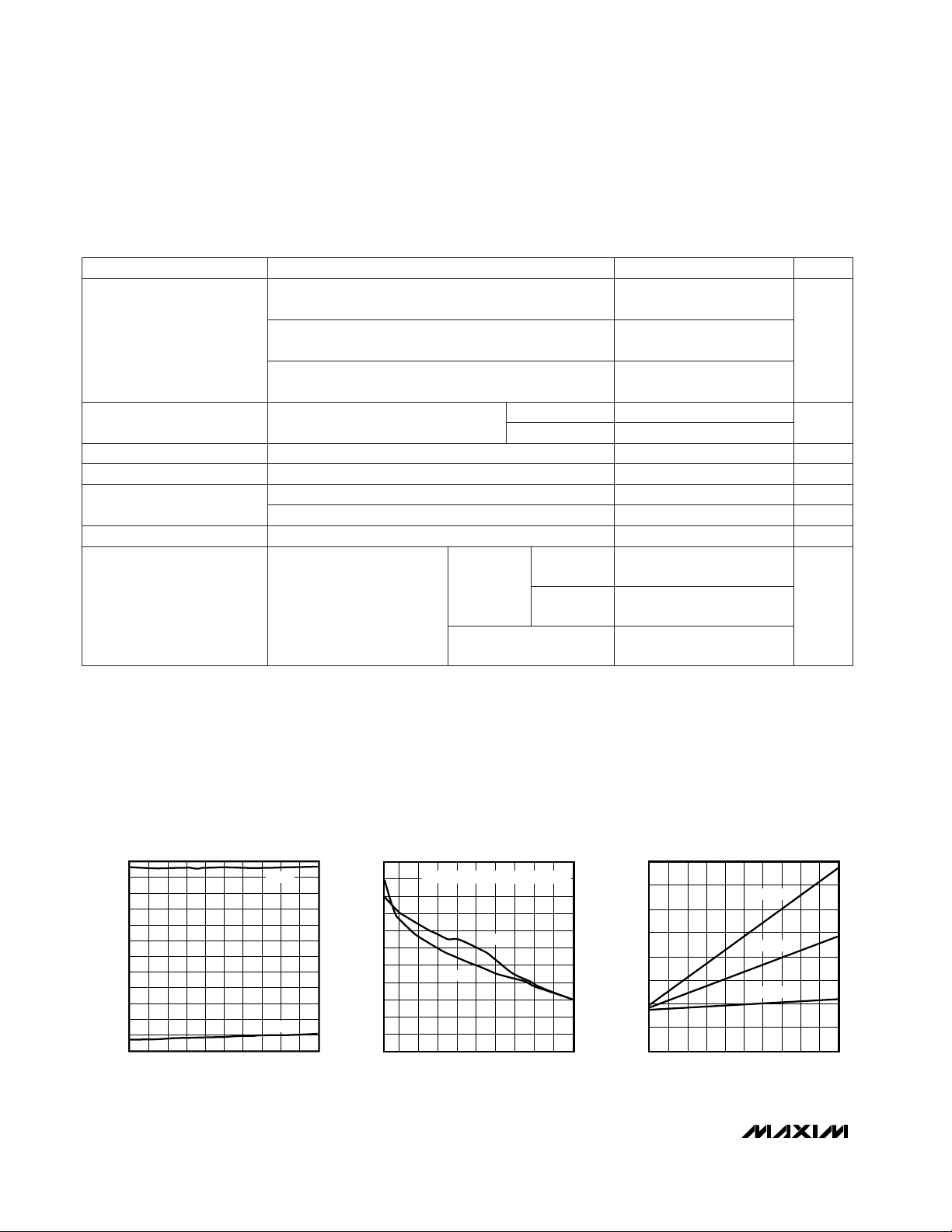
__________________________________________Typical Operating Characteristics
(VCC= +3.3V, 235kbps data rate, 0.1µF capacitors, all transmitters loaded with 3kΩ, TA= +25°C, unless otherwise noted.)
-6
-5
-4
-3
-2
-1
0
1
2
3
4
5
6
0
MAX3222/MAX3232
TRANSMITTER OUTPUT VOLTAGE
vs. LOAD CAPACITANCE
MAX3222-01
LOAD CAPACITANCE (pF)
TRANSMITTER OUTPUT VOLTAGE (V)
2000 30001000 4000 5000
V
OUT
+
V
OUT
-
0
2
4
6
8
10
12
14
16
18
20
22
150
MAX3222/MAX3232
SLEW RATE
vs. LOAD CAPACITANCE
MAX3222-02
LOAD CAPACITANCE (pF)
SLEW RATE (V/µs)
2000 30001000 4000 5000
FOR DATA RATES UP TO 235kbps
+SLEW
-SLEW
0
5
10
15
20
25
30
35
40
0
MAX3222/MAX3232
SUPPLY CURRENT vs. LOAD CAPACITANCE
WHEN TRANSMITTING DATA
MAX3222-03
LOAD CAPACITANCE (pF)
SUPPLY CURRENT (mA)
2000 30001000 4000 5000
235kbps
120kbps
20kbps
RL= 3kΩ, CL= 1000pF, one transmitter switching,
MBAUD = GND
Normal operation
CONDITIONS
Normal operation ns200Receiver Output Disable Time
| t
PHL
- t
PLH
|, MBAUD = GND
ns100
0.15
250
µs
0.15
Receiver Propagation Delay
ns200Receiver Output Enable Time
UNITS
MIN TYP MAX
PARAMETER
TIMING CHARACTERISTICS—MAX3237
(VCC= +3.0V to +5.5V, C1–C4 = 0.1µF (Note 2), TA= T
MIN
to T
MAX
, unless otherwise noted. Typical values are at TA= +25°C.)
VCC= 3.0V to 4.5V, RL= 3kΩ, CL= 250pF,
one transmitter switching, MBAUD = V
CC
1000
VCC= 4.5V to 5.5V, RL= 3kΩ, CL= 1000pF,
one transmitter switching, MBAUD = V
CC
kbps
1000
Maximum Data Rate
R_IN to R_OUT, CL= 150pF
| t
PHL
- t
PLH
|, MBAUD = V
CC
ns25
Transmitter Skew
| t
PHL
- t
PLH
|
ns50Receiver Skew
630
V/µs
430
t
PHL
t
PLH
CL= 150pF to 2500pF,
MBAUD = GND
CL= 150pF
to 1000pF
MBAUD =
GND
VCC= 3.3V, RL= 3Ω to 7kΩ,
+3V to -3V or -3V to +3V,
TA= +25°C
Transition-Region Slew Rate
MBAUD =
V
CC
24 150
Note 2: MAX3222/MAX3232/MAX3241: C1–C4 = 0.1µF tested at 3.3V ±10%; C1 = 0.047µF, C2–C4 = 0.33µF tested at 5.0V ±10%.
MAX3237: C1–C4 = 0.1µF tested at 3.3V ±5%; C1–C4 = 0.22µF tested at 3.3V ±10%; C1 = 0.047µF, C2–C4 = 0.33µF tested
at 5.0V ±10%.
Note 3: Transmitter input hysteresis is typically 250mV.
Page 5
MAX3222/MAX3232/MAX3237/MAX3241
3.0V to 5.5V, Low-Power, up to 1Mbps, True RS-232
Transceivers Using Four 0.1µF External Capacitors
_______________________________________________________________________________________
5
-7.5
-5.0
-2.5
0
2.5
5.0
7.5
0
MAX3241
TRANSMITTER OUTPUT VOLTAGE
vs. LOAD CAPACITANCE
MAX3222-04
LOAD CAPACITANCE (pF)
TRANSMITTER OUTPUT VOLTAGE (V)
2000 30001000 4000 5000
V
OUT
+
1 TRANSMITTER AT 235kbps
2 TRANSMITTERS AT 30kbps
V
OUT
-
ALL OUTPUTS LOADED WITH 3kΩ +CL
0.1µF CHARGE-PUMP CAPACITORS
FOR ALL DATA RATES UP TO 235kbps
4
6
8
10
12
14
16
18
20
22
24
0
MAX3241
SLEW RATE
vs. LOAD CAPACITANCE
MAX3222-05
LOAD CAPACITANCE (pF)
SLEW RATE (V/µs)
2000 30001000 4000 5000
+SLEW
-SLEW
0
5
10
15
20
25
30
35
45
40
0
MAX3241
SUPPLY CURRENT vs. LOAD
CAPACITANCE WHEN TRANSMITTING DATA
MAX3222-06
LOAD CAPACITANCE (pF)
SUPPLY CURRENT (mA)
2000 30001000 4000 5000
235kbps
120kbps
20kbps
-7.5
-5.0
-2.5
0
2.5
5.0
7.5
0
MAX3237
TRANSMITTER OUTPUT VOLTAGE
vs. LOAD CAPACITANCE (MBAUD = GND)
MAX3222-07
LOAD CAPACITANCE (pF)
TRANSMITTER OUTPUT VOLTAGE (V)
2000 30001000 4000 5000
1 TRANSMITTER AT 240kbps
4 TRANSMITTERS AT 15kbps
3kΩ + C
L
LOADS
V
CC
= 3.3V
0
10
20
30
50
40
60
70
0
MAX3237
SLEW RATE vs. LOAD CAPACITANCE
(MBAUD = V
CC
)
MAX3222-10
LOAD CAPACITANCE (pF)
SLEW RATE (V/µs)
500 1000 1500 2000
-SLEW, 1Mbps
+SLEW, 1Mbps
1 TRANSMITTER AT FULL DATA RATE
4 TRANSMITTERS AT 1/16 DATA RATE
3kΩ + C
L
LOAD EACH OUTPUT
V
CC
= 3.3V
-SLEW, 2Mbps
+SLEW, 2Mbps
-7.5
-5.0
-2.5
0
2.5
5.0
7.5
0
MAX3237
TRANSMITTER OUTPUT VOLTAGE
vs. LOAD CAPACITANCE (MBAUD = V
CC
)
MAX3222-08
LOAD CAPACITANCE (pF)
TRANSMITTER OUTPUT VOLTAGE (V)
500 1000 1500 2000
1 TRANSMITTER AT FULL DATA RATE
4 TRANSMITTERS AT 1/16 DATA RATE
3kΩ + C
L
LOAD, EACH OUTPUT
V
CC
= 3.3V
2Mbps
1.5Mbps
1Mbps
2Mbps
1Mbps
1.5Mbps
0
10
20
30
40
50
60
0
MAX3237
SUPPLY CURRENT vs.
LOAD CAPACITANCE (MBAUD = GND)
MAX3222-11
LOAD CAPACITANCE (pF)
SUPPLY CURRENT (mA)
2000 30001000 4000 5000
240kbps
120kbps
20kbps
1 TRANSMITTER AT FULL DATA RATE
4 TRANSMITTERS AT 1/16 DATA RATE
3kΩ + C
L
LOADS
V
CC
= 3.3V
0
2
4
6
8
10
12
0
MAX3237
SLEW RATE vs. LOAD CAPACITANCE
(MBAUD = GND)
MAX3222-09
LOAD CAPACITANCE (pF)
SLEW RATE (V/µs)
2000 30001000 4000 5000
+SLEW
-SLEW
1 TRANSMITTER AT 240kbps
4 TRANSMITTERS AT 15kbps
3kΩ + C
L
LOADS
V
CC
= 3.3V
0
10
30
20
40
50
60
70
0
MAX3237
SKEW vs. LOAD CAPACITANCE
(t
PLH
- t
PHL
)
MAX3222-12
LOAD CAPACITANCE (pF)
1000 1500500 2000 2500
MAX
MIN
AVERAGE; 10 PARTS
SKEW (ns)
1 TRANSMITTER AT 512kbps
4 TRANSMITTERS AT 32kbps
3kΩ + C
L
LOADS
V
CC
= 3.3V
MBAUD = V
CC
_____________________________Typical Operating Characteristics (continued)
(VCC= +3.3V, 235kbps data rate, 0.1µF capacitors, all transmitters loaded with 3kΩ, TA= +25°C, unless otherwise noted.)
Page 6

MAX3222/MAX3232/MAX3237/MAX3241
3.0V to 5.5V, Low-Power, up to 1Mbps, True RS-232
Transceivers Using Four 0.1µF External Capacitors
6 _______________________________________________________________________________________
—
FUNCTION
—
MAX3222
Noninverting Complementary Receiver Outputs.
Always active.
DIP/SO SSOP
— 11, 14
1 1 Receiver Enable. Active low.
2 2
Positive Terminal of Voltage-Doubler Charge-Pump
Capacitor
6 6
Negative Terminal of Inverting Charge-Pump
Capacitor
5 5
Positive Terminal of Inverting Charge-Pump
Capacitor
4 4
Negative Terminal of Voltage-Doubler Charge-Pump
Capacitor
3 3 +5.5V Generated by the Charge Pump
11, 12 12, 13 TTL/CMOS Transmitter Inputs
10, 13 10, 15 TTL/CMOS Receiver Outputs
9, 14 9, 16 RS-232 Receiver Inputs
8, 15 8, 17 RS-232 Transmitter Outputs
7 7 -5.5V Generated by the Charge Pump
18 20 Shutdown Control. Active low.
17 19 +3.0V to +5.5V Supply Voltage
16 18 Ground
No Connection
MAX3237MAX3232
— 16
— 13
1 28
5 3
4 1
3 25
2 27
10, 11
17, 19, 22,
23, 24
9, 12 18, 20, 21
8, 13 8, 9, 11
7, 14
5, 6, 7,
10, 12
6 4
— 14
16 26
15 2
— —
NAME
EN
C1+
C2-
C2+
C1-
V+
T_IN
R_OUT
R_IN
T_OUT
V-
SHDN
V
CC
GND
R_OUTB
N.C.
MAX3241
20, 21
23
28
2
1
24
27
12, 13, 14
15–19
4–8
9, 10, 11
3
22
26
25
—
PIN
— —
MegaBaud Control Input. Connect to GND for normal
operation; connect to VCCfor 1Mbps transmission rates.
— 15 MBAUD—
______________________________________________________________Pin Description
Page 7

MAX3222/MAX3232/MAX3237/MAX3241
3.0V to 5.5V, Low-Power, up to 1Mbps, True RS-232
Transceivers Using Four 0.1µF External Capacitors
_______________________________________________________________________________________ 7
_______________Detailed Description
Dual Charge-Pump Voltage Converter
The MAX3222/MAX3232/MAX3237/MAX3241’s internal
power supply consists of a regulated dual charge pump
that provides output voltages of +5.5V (doubling charge
pump) and -5.5V (inverting charge pump), regardless of
the input voltage (VCC) over the 3.0V to 5.5V range. The
charge pumps operate in a discontinuous mode; if the
output voltages are less than 5.5V, the charge pumps
are enabled, and if the output voltages exceed 5.5V, the
charge pumps are disabled. Each charge pump
requires a flying capacitor (C1, C2) and a reservoir
capacitor (C3, C4) to generate the V+ and V- supplies.
RS-232 Transmitters
The transmitters are inverting level translators that convert CMOS-logic levels to 5.0V EIA/TIA-232 levels.
The MAX3222/MAX3232/MAX3241 transmitters guarantee a 120kbps data rate with worst-case loads of 3kΩ in
parallel with 1000pF, providing compatibility with PC-toPC communication software (such as LapLink™).
Typically, these three devices can operate at data rates
of 235kbps. Transmitters can be paralleled to drive multiple receivers or mice.
The MAX3222/MAX3237/MAX3241’s output stage is
turned off (high impedance) when the device is in shutdown mode. When the power is off, the MAX3222/
MAX3232/MAX3237/MAX3241 permit the outputs to be
driven up to ±12V.
The transmitter inputs do not have pull-up resistors.
Connect unused inputs to GND or V
CC
.
MAX3237 MegaBaud Operation
In normal operating mode (MBAUD = GND), the
MAX3237 transmitters guarantee a 250kbps data rate
with worst-case loads of 3kΩ in parallel with 1000pF.
This provides compatibility with PC-to-PC communication software, such as Laplink™.
For higher speed serial communications, the MAX3237
features MegaBaud operation. In MegaBaud operating
mode (MBAUD = VCC), the MAX3237 transmitters guarantee a 1Mbps data rate with worst-case loads of 3kΩ in
parallel with 250pF for 3.0V < V
CC
< 4.5V. For 5V ±10%
operation, the MAX3237 transmitters guarantee a 1Mbps
data rate into worst-case loads of 3kΩ in parallel with
1000pF.
MAX3222
MAX3232
MAX3237
MAX3241
5k
R_ IN
R_ OUT
EN
*
C2-
C2+
C1-
C1+
V-
V+
V
CC
C4
C3
C1
C2
0.1µF
V
CC
SHDN*
T_ OUT
T_ IN
GND
V
CC
0V
7k
150pF
MAX3222
MAX3232
MAX3237
MAX3241
5k
R_ IN
R_ OUT
EN
*
C2-
C2+
C1-
C1+
V-
V+
V
CC
C4
C3
C1
C2
0.1µF
V
CC
SHDN*
T_ OUT
T_ IN
GND
V
CC
0V
3k
2500pF
MINIMUM SLEW-RATE TEST CIRCUIT MAXIMUM SLEW-RATE TEST CIRCUIT
* MAX3222/MAX3241 ONLY
Figure 1. Slew-Rate Test Circuits
LapLink is a trademark of Traveling Software.
Page 8
MAX3222/MAX3232/MAX3237/MAX3241
3.0V to 5.5V, Low-Power, up to 1Mbps, True RS-232
Transceivers Using Four 0.1µF External Capacitors
8 _______________________________________________________________________________________
RS-232 Receivers
The receivers convert RS-232 signals to CMOS-logic output levels. The MAX3222/MAX3237/MAX3241 receivers
have inverting three-state outputs. In shutdown, the
receivers can be active or inactive (Table 1).
The complementary outputs on the MAX3237 (R1OUTB)
and the MAX3241 (R1OUTB, R2OUTB) are always active,
regardless of the state of EN or SHDN. This allows for
Ring Indicator applications without forward biasing other
devices connected to the receiver outputs. This is ideal
for systems where VCCis set to 0V in shutdown to
accommodate peripherals, such as UARTs (Figure 2).
MAX3222/MAX3237/MAX3241
Shutdown Mode
Supply current falls to less than 1µA in shutdown mode
(SHDN = low). When shut down, the device’s charge
pumps are turned off, V+ is pulled down to VCC, V- is
pulled to ground, and the transmitter outputs are disabled (high impedance). The time required to exit shutdown is typically 100µs, as shown in Figure 3. Connect
SHDN to VCCif the shutdown mode is not used. SHDN
has no effect on R_OUT or R_OUTB.
MAX3222/MAX3237/MAX3241
Enable Control
The inverting receiver outputs (R_OUT) are put into a
high-impedance state when EN is high. The complementary outputs R1OUTB and R2OUTB are always active,
regardless of the state of EN and SHDN (Table 1). EN
has no effect on T_OUT.
__________Applications Information
Capacitor Selection
The capacitor type used for C1–C4 is not critical for
proper operation; polarized or nonpolarized capacitors
can be used. The charge pump requires 0.1µF capacitors for 3.3V operation. For other supply voltages, refer to
Table 2 for required capacitor values. Do not use values
lower than those listed in Table 2. Increasing the capacitor values (e.g., by a factor of 2) reduces ripple on the
transmitter outputs and slightly reduces power consumption. C2, C3, and C4 can be increased without changing
C1’s value. However, do not increase C1 without also
increasing the values of C2, C3, and C4, to maintain the
proper ratios (C1 to the other capacitors).
When using the minimum required capacitor values,
make sure the capacitor value does not degrade excessively with temperature. If in doubt, use capacitors with a
higher nominal value. The capacitor’s equivalent series
resistance (ESR), which usually rises at low temperatures, influences the amount of ripple on V+ and V-.
MAX3237
MAX3241
T1OUT
R1OUTB
Tx
5k
UART
V
CC
T1IN
LOGIC
TRANSITION
DETECTOR
R1IN
R1OUT
EN = V
CC
SHDN = GND
V
CC
TO
µP
Rx
PREVIOUS
RS-232
Tx
UART
PROTECTION
DIODE
PROTECTION
DIODE
SHDN = GND
V
CC
V
CC
GND
Rx
5k
a) OLDER RS-232: POWERED-DOWN UART DRAWS CURRENT FROM
ACTIVE RECEIVER OUTPUT IN SHUTDOWN.
b) NEW MAX3237/MAX3241: EN SHUTS DOWN RECEIVER OUTPUTS (EXCEPT FOR
B OUTPUTS), SO NO CURRENT FLOWS TO UART IN SHUTDOWN. B OUTPUTS
INDICATE RECEIVER ACTIVITY DURING SHUTDOWN WITH EN HIGH.
GND
Figure 2. Detection of RS-232 Activity when the UART and
Interface are Shut Down; Comparison of MAX3237/MAX3241
(b) with Previous Transceivers (a).
Page 9

MAX3222/MAX3232/MAX3237/MAX3241
3.0V to 5.5V, Low-Power, up to 1Mbps, True RS-232
Transceivers Using Four 0.1µF External Capacitors
_______________________________________________________________________________________ 9
Power-Supply Decoupling
In most circumstances, a 0.1µF bypass capacitor is
adequate. In applications that are sensitive to powersupply noise, decouple VCCto ground with a capacitor
of the same value as charge-pump capacitor C1. Connect
bypass capacitors as close to the IC as possible.
Operation Down to 2.7V
Transmitter outputs will meet EIA/TIA-562 levels of
±3.7V with supply voltages as low as 2.7V.
Transmitter Outputs when
Exiting Shutdown
Figure 3 shows two transmitter outputs when exiting
shutdown mode. As they become active, the two transmitter outputs are shown going to opposite RS-232 levels (one transmitter input is high, the other is low).
Each transmitter is loaded with 3kΩ in parallel with
2500pF. The transmitter outputs display no ringing or
undesirable transients as they come out of shutdown.
Note that the transmitters are enabled only when the
magnitude of V- exceeds approximately 3V.
Mouse Driveability
The MAX3241 has been specifically designed to power
serial mice while operating from low-voltage power supplies. It has been tested with leading mouse brands from
manufacturers such as Microsoft and Logitech. The
MAX3241 successfully drove all serial mice tested and
met their respective current and voltage requirements.
Figure 4a shows the transmitter output voltages under
increasing load current at 3.0V. Figure 4b shows a typical
mouse connection using the MAX3241.
Table 1. MAX3222/MAX3237/MAX3241
Shutdown and Enable Control Truth Table
Table 2. Required Minimum Capacitor Values
5V/div
V
CC
= 3.3V
C1–C4 = 0.1µF
2V/div
T2
50µs/div
T1
Figure 3. Transmitter Outputs when Exiting Shutdown or
Powering Up
V
CC
(V)
C1
(µF)
4.5 to 5.5 0.047
3.0 to 5.5 0.1
C2, C3, C4
(µF)
MAX3222/MAX3232/MAX3241
0.33
0.47
1 Active
0
1
Active1
SSHHDDNN
High-Z10
High-Z00
T_OUT
EENN
High-Z
Active
High-Z
Active
R_OUT
R_OUTB
(MAX3237/
MAX3241)
Active
Active
Active
Active
3.0 to 3.6 0.22
3.15 to 3.6 0.1
MAX3237
0.22
0.1
4.5 to 5.5 0.047
3.0 to 5.5 0.22
0.33
1.0
3.0 to 3.6 0.1 0.1
Page 10
MAX3222/MAX3232/MAX3237/MAX3241
3.0V to 5.5V, Low-Power, up to 1Mbps, True RS-232
Transceivers Using Four 0.1µF External Capacitors
10 ______________________________________________________________________________________
MAX3241
EN
23
R5OUT
15
R4OUT
16
R3OUT
17
R2OUT
18
R1OUT
19
R2OUTB
20
R1OUTB
21
5k
5k
5k
5k
5k
R5IN 8
R4IN
7
6
R2IN 5
R1IN 4
SHDN
22
GND
25
T3IN
12
T2IN
13
T1IN
14
C2-
2
C2+
1
C1-
24
C1+
28
T3OUT
11
+V
COMPUTER SERIAL PORT
MOUSE
+V
-V
GND
Tx
T2OUT
10
T1OUT
9
V-
3
V+
27
V
CC
V
CC
C4
C3 C
1
C
2
0.1µF
V
CC
= 3V
to 5.5V
26
R3IN
Figure 4b. Mouse Driver Test Circuit
-6
-5
-4
-3
-2
-1
0
1
2
3
4
5
6
01234567
MAX3222-04
LOAD CURRENT PER TRANSMITTER (mA)
TRANSMITTER OUTPUT VOLTAGE (V)
V
OUT
+
VCC = 3.0V
V
OUT
-
V
OUT
+
V
CC
V
OUT
-
T1
T2
T3
Figure 4a. MAX3241 Transmitter Output Voltage vs. Load Current per Transmitter
Page 11

MAX3222/MAX3232/MAX3237/MAX3241
3.0V to 5.5V, Low-Power, up to 1Mbps, True RS-232
Transceivers Using Four 0.1µF External Capacitors
______________________________________________________________________________________ 11
High Data Rates
The MAX3222/MAX3232/MAX3241 maintain the RS-232
±5.0V minimum transmitter output voltage even at high
data rates. Figure 5 shows a transmitter loopback test
circuit. Figure 6 shows a loopback test result at
120kbps, and Figure 7 shows the same test at 235kbps.
For Figure 6, all transmitters were driven simultaneously
at 120kbps into RS-232 loads in parallel with 1000pF.
For Figure 7, a single transmitter was driven at 235kbps,
and all transmitters were loaded with an RS-232 receiver
in parallel with 1000pF.
The MAX3237 maintains the RS-232 ±5.0V minimum
transmitter output voltage at data rates up to 1Mbps.
Figure 8 shows a loopback test result at 1Mbps with
MBAUD = VCC. For Figure 8, all transmitters were
loaded with an RS-232 receiver in parallel with 250pF.
MAX3222
MAX3232
MAX3237
MAX3241
5k
R_ IN
R_ OUT
EN
*
C2-
C2+
C1-
C1+
V-
V+
V
CC
C4
C3
C1
C2
0.1µF
V
CC
SHDN*
T_ OUT
T_ IN
GND
V
CC
0V
1000pF
* MAX3222/MAX3241 ONLY
Figure 5. Loopback Test Circuit
Figure 6. MAX3241 Loopback Test Result at 120kbps
T1IN
R1OUT
V
CC
= 3.3V
T1OUT
5V/div
5V/div
2µs/div
5V/div
Figure 7. MAX3241 Loopback Test Result at 235kbps
+5V
0V
+5V
0V
-5V
+5V
0V
T_IN
T_OUT = R_IN
5k + 250pF
R_OUT
150pF
200ns/div
VCC = 3.3V
Figure 8. MAX3237 Loopback Test Result at 1000kbps
(MBAUD = V
CC
)
T1IN
T1OUT
R1OUT
5µs/div
= 3.3V
V
CC
5V/div
5V/div
5V/div
Page 12
MAX3222/MAX3232/MAX3237/MAX3241
3.0V to 5.5V, Low-Power, up to 1Mbps, True RS-232
Transceivers Using Four 0.1µF External Capacitors
12 ______________________________________________________________________________________
__________________________________________________Typical Operating Circuits
MAX3222
R2OUT10
1
R1OUT13
R2IN
9
18
GND
16
RS-232
OUTPUTS
TTL/CMOS
INPUTS
T2IN
11
T1IN
12
C2-
6
C2+
5
C1-
4
C1+
2
R1IN
14
T2OUT
8
T1OUT
15
V-
7
V+
3
V
CC
17
C1
0.1µF
C2
0.1µF
0.1µF
+3.3V
RS-232
INPUTS
TTL/CMOS
OUTPUTS
5k
5k
EN
SHDN
C3*
0.1µF
C4
0.1µF
PIN NUMBERS REFER TO DIP/SO PACKAGES.
* C3 CAN BE RETURNED TO EITHER V
CC
OR GROUND.
MAX3232
R2OUT9
R1OUT12
R2IN
8
GND
15
RS-232
OUTPUTS
TTL/CMOS
INPUTS
T2IN
10
T1IN
11
C2-
5
C2+
4
C1-
3
C1+
1
R1IN
13
T2OUT
7
T1OUT
14
V-
6
V+
2
V
CC
C4
0.1µF
16
0.1µF
0.1µF
0.1µF
+3.3V
RS-232
INPUTS
TTL/CMOS
OUTPUTS
C3*
0.1µF
5k
5k
* C3 CAN BE RETURNED TO EITHER V
CC
OR GROUND.
SEE TABLE 2 FOR CAPACITOR SELECTION
Interconnection with 3V and 5V Logic
The MAX3222/MAX3232/MAX3237/MAX3241 can
directly interface with various 5V logic families, including ACT and HCT CMOS. See Table 3 for more information on possible combinations of interconnections.
Table 3. Logic-Family Compatibility
with Various Supply Voltages
Compatible with ACT and
HCT CMOS, and with TTL.
Incompatible with AC, HC,
and CD4000 CMOS.
3.35
SYSTEM
POWERSUPPLY
VOLTAGE
(V)
Compatible with all TTL
and CMOS-logic families.
55
Compatible with all CMOS
families.
3.33.3
COMPATIBILITY
MAX32_ _
V
CC
SUPPLY
VOLTAGE
(V)
Page 13

MAX3222/MAX3232/MAX3237/MAX3241
3.0V to 5.5V, Low-Power, up to 1Mbps, True RS-232
Transceivers Using Four 0.1µF External Capacitors
______________________________________________________________________________________ 13
_____________________________________Typical Operating Circuits (continued)
MAX3241
EN
23
R5OUT
15
R4OUT
16
R3OUT
17
R2OUT
18
R1OUT
19
R2OUTB
20
R1OUTB
21
TTL/CMOS
OUTPUTS
5k
5k
5k
5k
5k
R5IN 8
* C3 CAN BE RETURNED TO EITHER V
CC
OR GROUND.
R4IN
7
R3IN
6
R2IN 5
R1IN
4
RS-232
INPUTS
SHDN
22
GND
25
RS-232
OUTPUTS
TTL/CMOS
INPUTS
T3IN
12
T2IN
13
T1IN
14
C2-
2
C2+
1
C1-
24
C1+
28
T3OUT
11
T2OUT 10
T1OUT 9
V-
3
V+
27
V
CC
C4
0.1µF
C3
*
0.1µF
0.1µF
0.1µF
0.1µF
+3.3V
26
0.1µF
0.1µF
0.1µF
LOGIC
INPUTS
LOGIC
OUTPUTS
26
V
28
C1+
25
C1-
1
C2+
3
C2T1IN
24
T2IN
23
T3IN
22
T4IN
19
T5IN
17
R1OUTB
16
R1OUT
21
R2OUT
20
R3OUT
18
CC
MAX3237
T1
T2
T3
T4
T5
R1
R2
R3
V+
V-
T1OUT 5
T2OUT 6
T3OUT
T4OUT 10
T5OUT
R1IN
5k
R2IN 9
5k
R3IN
5k
0.1µF
27
4
0.1µF
7
RS-232
OUTPUTS
12
8
RS-232
INPUTS
11
15
2
MBAUD
SHDN
OR GROUND.
CC
14
EN
13
GND
* C3 CAN BE RETURNED TO EITHER V
Page 14

MAX3222/MAX3232/MAX3237/MAX3241
3.0V to 5.5V, Low-Power, up to 1Mbps, True RS-232
Transceivers Using Four 0.1µF External Capacitors
14 ______________________________________________________________________________________
_____________________________________________Pin Configurations (continued)
16
15
14
13
12
11
10
9
1
2
3
4
5
6
7
8
V
CC
GND
T1OUT
R1INC2+
C1-
V+
C1+
MAX3232
R1OUT
T1IN
T2IN
R2OUTR2IN
T2OUT
V-
C2-
DIP/SO/TSSOP
TOP VIEW
20
19
18
17
16
15
14
13
1
2
3
8
12
11
10
4
5
6
7
SHDN
V
CC
GND
T1OUT
C1-
V+
C1+
EN
R1IN
R1OUT
T1IN
T2IN
T2OUT
V-
C2-
C2+
9
R2IN
R2OUT
SSOP/TSSOP
N.C.
N.C.
MAX3222
28
27
26
25
24
23
22
21
20
19
18
17
16
15
1
2
3
4
5
6
7
8
9
10
11
12
13
14
C1+
V+
V
CC
C1T1IN
T2IN
MBAUD
T3IN
R1OUT
R2OUT
T4IN
R3OUT
T5IN
R1OUTB
SHDN
EN
T5OUT
R3IN
T4OUT
R2IN
R1IN
T3OUT
T2OUT
T1OUT
V-
C2-
GND
C2+
SSOP
MAX3237
28
27
26
25
24
23
22
21
20
19
18
17
16
15
1
2
3
4
5
6
7
8
9
10
11
12
13
14
C1+
V+
V
CC
GND
C1-
EN
R5OUT
SHDN
R1OUTB
R2OUTB
R1OUT
R2OUT
R3OUT
R4OUT
T1IN
T2IN
T3IN
T3OUT
T2OUT
T1OUT
R5IN
R4IN
R3IN
R2IN
R1IN
V-
C2-
C2+
SO/SSOP/TSSOP
MAX3241
Page 15

MAX3222/MAX3232/MAX3237/MAX3241
3.0V to 5.5V, Low-Power, up to 1Mbps, True RS-232
Transceivers Using Four 0.1µF External Capacitors
______________________________________________________________________________________ 15
______3V-Powered EIA/TIA-232 and EIA/TIA-562 Transceivers from Maxim
Ordering Information (continued)
* Dice are tested at TA= +25°C, DC parameters only.
0.1µF capacitors, 1 complementary receiver, MegaBaud
operation
232250/100035/33.0 to 5.5MAX3237
0.1µF capacitors, AutoShutdown,
complementary receiver,
drives mice
23212013/53.0 to 5.5MAX3243
0.1µF capacitors232120N/A2/23.0 to 5.5MAX3232
0.1µF capacitors, AutoShutdown23212022/23.0 to 5.5MAX3223
0.1µF capacitors23212022/23.0 to 5.5MAX3222
232
562
232
562
232
EIA/
TIA-232
OR 562
2.7 to 3.6
AutoShutdown, complementary
receiver, drives mice, transient
detection
23553/5MAX3212
0.1µF capacitors23022/23.0 to 3.6MAX563
Operates directly from batteries
without a voltage regulator
12022/21.8 to 4.25MAX218
No. OF
RECEIVERS
ACTIVE IN
SHUTDOWN
POWER-
SUPPLY
VOLTAGE
(V)
Wide supply range23053/52.7 to 5.25MAX562
Drives mice12053/53.0 to 3.6MAX212
FEATURES
GUAR-
ANTEED
DATA
RATE
(kbps)
No. OF
TRANSMITTERS/
RECEIVERS
PART
0.1µF capacitors, 2 complementary receivers, drives mice
23212053/53.0 to 5.5MAX3241
PART
MAX3222EUP
MAX3222EAP
MAX3222EWN -40°C to +85°C
-40°C to +85°C
-40°C to +85°C
TEMP. RANGE PIN-PACKAGE
20 TSSOP
20 SSOP
18 SO
MAX3222EPN
MAX3232CUE
MAX3232CSE 0°C to +70°C
0°C to +70°C
-40°C to +85°C 18 Plastic DIP
16 TSSOP
16 Narrow SO
MAX3232CWE
MAX3232EUE
MAX3232ESE -40°C to +85°C
-40°C to +85°C
0°C to +70°C 16 Wide SO
16 TSSOP
16 Narrow SO
MAX3222C/D 0°C to +70°C Dice*
MAX3232CPE 0°C to +70°C 16 Plastic DIP
PART TEMP. RANGE PIN-PACKAGE
MAX3232EWE
MAX3237CAI
MAX3237EAI -40°C to +85°C
0°C to +70°C
-40°C to +85°C 16 Wide SO
28 SSOP
28 SSOP
MAX3241CUI
0°C to +70°C 28 TSSOP
MAX3241CAI
MAX3241EUI
MAX3241EAI -40°C to +85°C
-40°C to +85°C
0°C to +70°C 28 SSOP
28 TSSOP
28 SSOP
MAX3241EWI -40°C to +85°C 28 SO
MAX3241CWI 0°C to +70°C 28 SO
MAX3232EPE -40°C to +85°C 16 Plastic DIP
Page 16

MAX3222/MAX3232/MAX3237/MAX3241
3.0V to 5.5V, Low-Power, up to 1Mbps, True RS-232
Transceivers Using Four 0.1µF External Capacitors
Maxim cannot assume responsibility for use of any circuitry other than circuitry entirely embodied in a Maxim product. No circuit patent licenses are
implied. Maxim reserves the right to change the circuitry and specifications without notice at any time.
16
____________________Maxim Integrated Products, 120 San Gabriel Drive, Sunnyvale, CA 94086 408-737-7600
© 1999 Maxim Integrated Products Printed USA is a registered trademark of Maxim Integrated Products.
___________________Chip Topography
___________________Chip Information
________________________________________________________Package Information
T1INT2IN
0.127"
(3.225mm)
0.087"
(2.209mm)
R2OUTR2INT2OUT
R1OUT
R1IN
T1OUT
V
CC
V+ C1+
SHDN
EN
C1-
C2+
C2-
V-
GND
MAX3222
TRANSISTOR COUNT: 339
SUBSTRATE CONNECTED TO GND
MAX3222 339
MAX3232 339
MAX3237 1212
MAX3241 894
TRANSISTOR COUNTPART
TSSOP.EPS
 Loading...