

_______________General Description
The MAX3320 combines a microprocessor (µP) supervisory circuit with an RS-232 transceiver. The power-on
reset performs a single function: it asserts a reset signal
whenever the VCCsupply voltage declines below a preset threshold, staying asserted for at least 100ms after
VCCrises above the reset threshold. The MAX3320 has
an active-low RESET output, which is guaranteed to be in
the correct state for VCCdown to 1V. The reset comparator is designed to ignore fast transients on VCC. Reset
thresholds suitable for operation with a variety of supply
voltages are available.
The MAX3320 transceivers have a proprietary lowdropout transmitter output stage, enabling true RS-232
performance with a dual charge pump powered from a
+3V to +5.5V supply. The device requires only four
small 0.1µF external charge-pump capacitors, and is
guaranteed to run at data rates of up to 250kbps. It
comes in the space-saving 20-pin SSOP package.
________________________Applications
Palmtop Computers
Portable/Battery-Powered Equipment
Hand-Held Equipment
Peripherals
Printers
____________________________Features
♦ Precise Monitoring of 5V and 3.3V Power-
Supply Voltages:
— 100ms (min) Power-On
RESET Pulse Width
— Power-Supply Transient Immunity
— Guaranteed RESET Valid to VCC= 1V
♦ 4µA Supply Current Achieved with
AutoShutdown Plus
♦ Receivers Always Active
♦ Power-On Reset Always Active
♦ 4µA Low-Power Shutdown
♦ 250kbps Guaranteed Data Rate
MAX3320A/B/L/T
3V to 5.5V, up to 250kbps True RS-232 T ransceiver
with 4µA AutoShutdown Plus and Power-On Reset
________________________________________________________________
Maxim Integrated Products
1
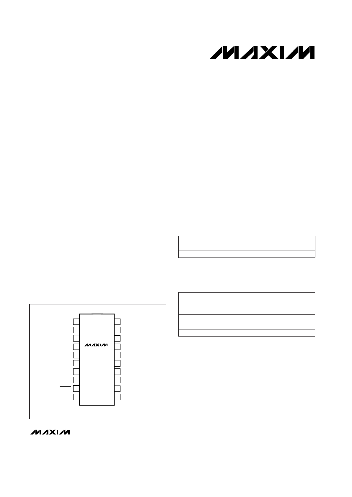
20
19
18
17
16
15
14
13
1
2
3
4
5
6
7
8
C1+
V
CC
C1GNDV-
C2-
C2+
V+
TOP VIEW
T1OUT
T2OUT
R1IN
R2INR2OUT
R1OUT
T2IN
T1IN
12
11
9
10
FORCEON
FORCEOFFRESET
INVALID
MAXxxx
SSOP
MAX3320
__________________Pin Configuration
19-1253; Rev 0; 8/97
PART*
MAX3320_CAP
MAX3320_EAP -40°C to +85°C
0°C to +70°C
TEMP. RANGE PIN-PACKAGE
20 SSOP
20 SSOP
______________Ordering Information
*
This part offers a choice of reset threshold voltage. From the
table below, select the suffix corresponding to the desired
threshold and insert it into the blank to complete the part
number.
AutoShutdown Plus is a trademark of Maxim Integrated Products.
SUFFIX
A
B
RESET THRESHOLD
(V)
4.25
2.85
L 4.63
T 3.08
Typical Operating Circuit appears at end of data sheet.
For free samples & the latest literature: http://www.maxim-ic.com, or phone 1-800-998-8800.
For small orders, phone 408-737-7600 ext. 3468.
MAX3320A/B/L/T
3V to 5.5V, up to 250kbps True RS-232 T ransceiver
with 4µA AutoShutdown Plus and Power-On Reset
2 _______________________________________________________________________________________
ABSOLUTE MAXIMUM RATINGS
ELECTRICAL CHARACTERISTICS
(VCC= 3V to 5.5V, C1–C4 = 0.1µF (tested at 3.3V ±10%), C1 = 0.047µF, C2–C4 = 0.33µF (tested at 5V ±10%), TA= T
MIN
to T
MAX
,
unless otherwise noted. Typical values are at T
A
= +25°C.)
Stresses beyond those listed under “Absolute Maximum Ratings” may cause permanent damage to the device. These are stress ratings only, and functional
operation of the device at these or any other conditions beyond those indicated in the operational sections of the specifications is not implied. Exposure to
absolute maximum rating conditions for extended periods may affect device reliability.
VCC.............................................................................-0.3V to 6V
V+ (Note 1) .................................................................-0.3V to 7V
V- (Note 1)...................................................................0.3V to -7V
V+ +
|V-|
(Note 1)...................................................................13V
Input Voltages
T_IN, FORCEOFF, FORCEON................................-0.3V to 6V
R_IN.................................................................................±25V
Output Voltages
T_OUT ..........................................................................±13.2V
R_OUT, INVALID, RESET.......................-0.3V to (V
CC
+ 0.3V)
Short-Circuit Duration
T_OUT....................................................................Continuous
Continuous Power Dissipation (TA= +70°C)
SSOP (derate 8.00mW/°C above +70°C)....................640mW
Operating Temperature Ranges
MAX3320_CAP...................................................0°C to +70°C
MAX3320_EAP................................................-40°C to +85°C
Storage Temperature Range.............................-65°C to +160°C
Lead Temperature (soldering, 10sec).............................+300°C
V-0.3 0.3Figure 3
Receiver Input Threshold to
INVALID Output Low
-2.7Figure 3, negative threshold
V
2.7Figure 3, positive threshold
Receiver Input Threshold to
INVALID Output High
kΩ
3 5 7TA= +25°CInput Resistance
V0.3Input Hysteresis
1.8 2.4VCC= 5V
V
1.5 2.4VCC= 3.3V
Input Threshold High
0.8 1.5VCC= 5V
V
0.6 1.2VCC= 3.3V
Input Threshold Low
V-25 25Input Voltage Range
µA4.0 10
FORCEOFF = GND, TA= +25°C
Shutdown Supply Current
mA0.45 1.0No load, VCC= 3.3V or 5V, TA= +25°CPower-Supply Current
V
VCC- V
CC -
0.6 0.1
I
OUT
= -1mAOutput Voltage High
V0.4I
OUT
= 1.6mAOutput Voltage Low
mV250
T_IN, FORCEON, FORCEOFF
Input Hysteresis
µA±0.01 ±1.0
T_IN, FORCEON, FORCEOFF
Input Leakage Current
µA4.0 10
All R_IN unconnected, FORCEON = GND,
FORCEOFF = V
CC
, all T_IN = VCCor GND, TA= +25°C
AutoShutdown Plus
Supply Current
V0.8
T_IN, FORCEON, FORCEOFF
Input Logic Threshold Low
V
2.0
Input Logic Threshold High
UNITSMIN TYP MAXCONDITIONSPARAMETER
T_IN, FORCEON,
FORCEOFF
2.4
V0.4I
OUT
= 1.6mA
INVALID Output Voltage Low
Note 1: V+ and V- can have a magnitude of +7V (max), but their absolute difference cannot exceed +13V.
VCC= 3.3V
VCC= 5V
DC CHARACTERISTICS
LOGIC INPUTS AND RECEIVER OUTPUTS
RECEIVER INPUTS
INVALID OUTPUT
MAX3320A/B/L/T
3V to 5.5V, up to 250kbps True RS-232 T ransceiver
with 4µA AutoShutdown Plus and Power-On Reset
_______________________________________________________________________________________ 3
sec15 30 60Figure 3
Receiver or Transmitter Edge
to Shutdown
µs25Figure 5
Receiver or Transmitter Edge
to Transmitters Enabled
90 µsFigure 3
Receiver Positive or Negative
Threshold to INVALID Low
µs0.1Figure 3
Receiver Positive or Negative
Threshold to INVALID High
UNITSMIN TYP MAXCONDITIONSPARAMETER
ELECTRICAL CHARACTERISTICS (continued)
(VCC= 3V to 5.5V, C1–C4 = 0.1µF (tested at 3.3V ±10%), C1 = 0.047µF, C2–C4 = 0.33µF (tested at 5V ±10%), TA= T
MIN
to T
MAX
,
unless otherwise noted. Typical values are at T
A
= +25°C.)
V±5.0 ±5.4
All transmitter outputs loaded with 3kΩ to ground
Output Voltage Swing
Ω
300 10MVCC= V+ = V- = GND, V
T_OUT
= ±2VOutput Resistance
mA±35 ±60T_OUT = GND, T_IN = VCCor GNDOutput Short-Circuit Current
µA±25V
T_OUT
= ±12V, VCC= 0 to 5.5V, transmitters disabledOutput Leakage Current
V
1.0 5.5MAX3320_C
RESET Operating Voltage
Range
1.2 5.5MAX3320_E
V
4.00 4.25 4.50MAX3320A
RESET Threshold
2.70 2.85 3.00MAX3320B
4.50 4.63 4.75MAX3320L
3.00 3.08 3.15MAX3320T
V
0.3I
SINK
= 1.2mA, VCC= reset threshold, MAX3320B/T
RESET Output Voltage
0.4I
SINK
= 3.2mA, VCC= reset threshold, MAX3320A/L
0.3I
SINK
= 50µA, VCC> 1V, MAX3320_C
0.4I
SINK
= 100µA, VCC> 1.2V, MAX3320_E
VVCC- 0.6I
OUT
= -1mA
INVALID Output Voltage High
AUTOSHUTDOWN PLUS (FORCEON = GND, FORCEOFF = VCC)
TRANSMITTER OUTPUTS
RESET OUTPUT
MAX3320A/B/L/T
3V to 5.5V, up to 250kbps True RS-232 T ransceiver
with 4µA AutoShutdown Plus and Power-On Reset
4 _______________________________________________________________________________________
-7.5
V
T_OUT-
V
T_OUT+
-2.5
-5.0
2.5
0
5.0
7.5
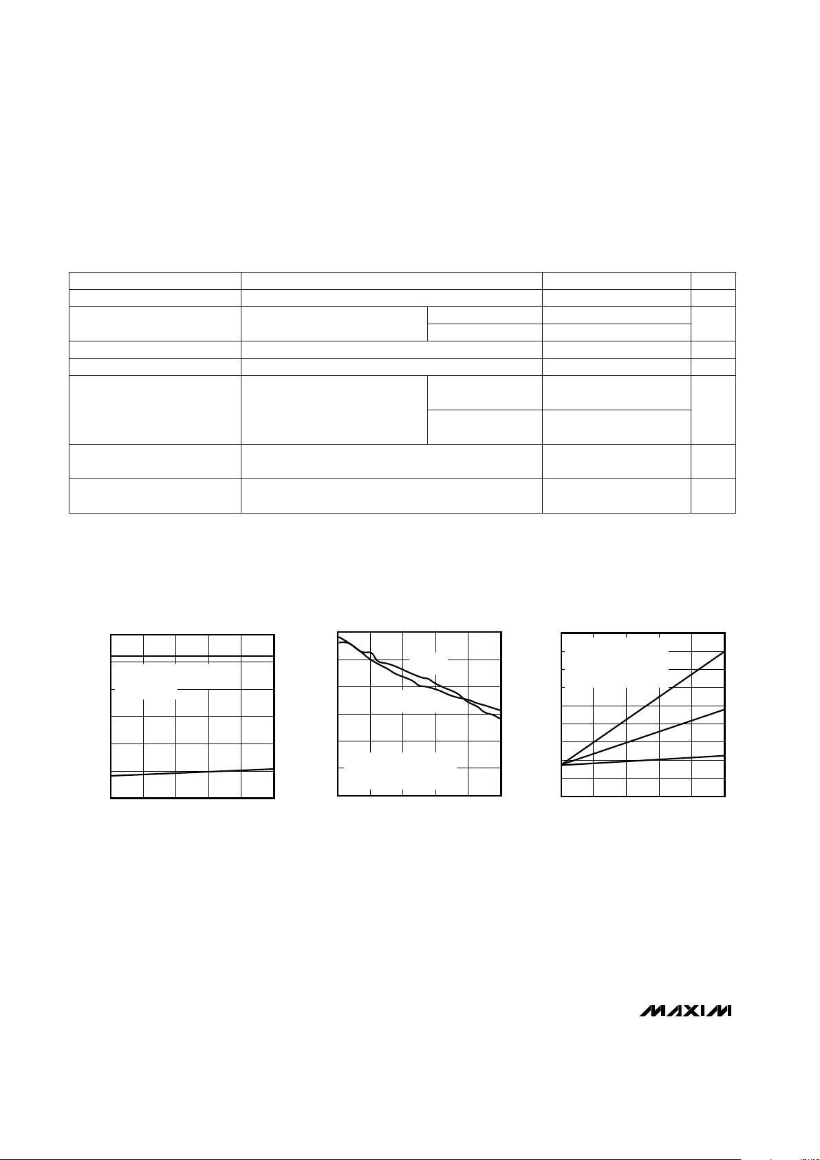
0 20001000 3000 4000 5000
TRANSMITTER OUTPUT VOLTAGE
vs. LOAD CAPACITANCE
MAX3320 TOC01
LOAD CAPACITANCE (pF)
OUTPUT VOLTAGE (V)
ONE TRANSMITTER AT 250kbps
ONE TRANSMITTER AT 15.6kbps
LOAD = 3kΩ + C
L
0
2
8
6
4
10
12
0 20001000 3000 4000 5000
SLEW RATE
vs. LOAD CAPACITANCE
MAX3320 TOC02
LOAD CAPACITANCE (pF)
SLEW RATE (V/us)
ONE TRANSMITTER AT 250kbps
ONE TRANSMITTER AT 15.6kbps
LOAD = 3kΩ + C
L
NEGATIVE
SLEW
POSITIVE
SLEW
0
250kbps
120kbps
20kbps
10
5
30
20
25
15
40
35
45
0 20001000 3000 4000 5000
SUPPLY CURRENT
vs. LOAD CAPACITANCE WHEN
TRANSMITTING DATA
MAX3320 TOC03
LOAD CAPACITANCE (pF)
SUPPLY CURRENT (mA)
ONE TRANSMITTER AT
FULL DATA RATE INDICATED
ONE TRANSMITTER AT
1/16 DATA RATE INDICATED
TIMING CHARACTERISTICS
(VCC= 3V to 5.5V, C1–C4 = 0.1µF, C1–C4 = 0.1µF (for 3.3V ±10%), C1 = 0.047µF, C2–C4 = 0.33µF (tested at 5V ±10%),
T
A
= T
MIN
to T
MAX
, unless otherwise noted. Typical values are at TA= +25°C.)
kbps250
RL= 3kΩ, CL= 1000pF, one transmitter switching
Maximum Data Rate
ns100
|
t
PHL
- t
PLH
|
Transmitter Skew
0.3
µs
0.3
R_IN to R_OUT, CL= 150pFReceiver Propagation Delay
UNITSMIN TYP MAXCONDITIONSPARAMETER
t
PLH
t
PHL
ns200
|
t
PHL
- t
PLH
|
Receiver Skew
CL= 150pF to
1000pf
V/µs
6 30
VCC= 3.3V, RL= 3kΩ to 7kΩ,
measured from +3V to -3V or -3V to
+3V, T
A
= +25°C
Transition-Region Slew Rate
ms100 280VCC= reset threshold
RESET Active Timeout Period
µs40100mV overdrive from reset threshold
VCCto RESET Delay
CL= 150pF to
2500pf
4 30
__________________________________________Typical Operating Characteristics
(VCC= 3.3V, 250kbps data rate, C1–C4 = 0.1µF, all transmitters loaded with 3kΩ. Typical values are at TA= +25°C, unless
otherwise noted.)

MAX3320A/B/L/T
3V to 5.5V, up to 250kbps True RS-232 T ransceiver
with 4µA AutoShutdown Plus and Power-On Reset
_______________________________________________________________________________________ 5
______________________________________________________________Pin Description
300
0
10 100 1000
MAXIMUM TRANSIENT DURATION
vs. RESET COMPARATOR OVERDRIVE
50
MAX3320toc05
RESET COMPARATOR OVERDRIVE (mV)
MAXIMUM TRANSIENT DURATION (µs)
100
200
150
250
NOT IN
SHUTDOWN
MODE
SHUTDOWN MODE
C
BYPASS
= 0.1µF
0.960
0.970
1.010
1.000
0.990
0.980
1.030
1.020
1.040
-40 0-20 20 40 8060
NORMALIZED POWER-UP RESET
DELAY vs. TEMPERATURE
MAX3320 TOC06
TEMPERATURE (°C)
POWER-UP RESET DELAY
____________________________Typical Operating Characteristics (continued)
(VCC= 3.3V, 250kbps data rate, C1–C4 = 0.1µF, all transmitters loaded with 3kΩ. Typical values are at TA= +25°C, unless
otherwise noted.)
20 C1+ Positive terminal of voltage-doubler charge-pump capacitor
19 V
CC
+3V to +5.5V Supply Voltage
18 C1- Negative terminal of voltage-doubler charge-pump capacitor
NAME FUNCTION
1 V+ 5.5V generated by the charge pump
2 C2+ Positive terminal of inverting charge-pump capacitor
PIN
3 C2- Negative terminal of inverting charge-pump capacitor
4 V- -5.5V generated by the charge pump
10
RESET
RESET Output. RESET remains low while VCCis below the reset threshold, and for 280ms (max)
after V
CC
rises above the reset threshold.
9
INVALID
Output of the Valid Signal Detector. Asserts when no valid RS-232 levels are present on any of
the receiver inputs for 90µs.
7, 8 R_OUT TTL/CMOS Receiver Outputs (R1OUT and R2OUT)
5, 6 T_IN TTL/CMOS Transmitter Inputs (T1IN and T2IN)
17 GND Ground
15, 16 T_OUT RS-232 Transmitter Outputs (T2OUT and T1OUT)
13, 14 R_IN RS-232 Receiver Inputs (R2IN and R1IN)
12 FORCEON
Force-On Input. Drive FORCEON high to override AutoShutdown Plus, keeping transmitters on
(FORCEOFF must be high) (Table 1).
11
FORCEOFF
Force-Off Input. Drive FORCEOFF low to shut down transmitters and on-board power supply.
This overrides AutoShutdown Plus and FORCEON (Table 1).

MAX3320A/B/L/T
6 _______________________________________________________________________________________
______________ Detailed Description
Dual Charge-Pump Voltage Converter
The MAX3320’s internal power supply consists of a regulated dual charge pump that provides output voltages
of +5.5V (doubling charge pump) and -5.5V (inverting
charge pump) while VCCremains in the 3V to 5.5V
range. The charge pumps operate in discontinuous
mode; they are enabled if the output voltages are less
than 5.5V, and disabled if output voltages exceed 5.5V.
Each charge pump requires a flying capacitor (C1, C2)
and a reservoir capacitor (C3, C4) to generate the V+
and V- supplies.
RS-232 Transmitters
The transmitters are inverting level translators that convert CMOS-logic levels to 5V EIA/TIA-232 levels. The
MAX3320 transmitters guarantee a 250kbps data rate
with worst-case loads of 3kΩ in parallel with 1000pF,
providing compatibility with PC-to-PC communication
software (such as LapLink™). Transmitters can be paralleled to drive multiple receivers. Figure 1 shows a
complete system connection.
When FORCEOFF is driven to ground, the transmitter’s
outputs become high impedance. When the
AutoShutdown Plus circuitry senses that all receiver
and transmitter inputs are inactive for more than 30sec,
the transmitters turn off and the outputs go into a highimpedance state, but the receivers remain active.
When the power is off or the MAX3320 is shut down,
outputs may be driven up to ±12V.
The transmitter inputs do not have pull-up resistors.
Connect unused inputs to GND or VCC.
Laplink is a trademark of Traveling Software.
RS-232 Receivers
The receivers convert RS-232 signals to CMOS-logic output levels. All receivers have inverting outputs and are
active in shutdown FORCEOFF (Table 1).
AutoShutdown Plus Mode
Maxim’s AutoShutdown Plus feature, which operates
when FORCEOFF is high and FORCEON is low, achieves
a 4µA supply current. When the MAX3320 senses no
valid signal levels on all receiver and transmitter inputs for
30sec, the on-board power supply and drivers shut off,
MAX3320
I/O
CHIP
WITH
UART
CPU
RS-232
POWER-
MANAGEMENT
UNIT OR
KEYBOARD
CONTROLLER
FORCEOFF
FORCEON
INVALID
T1
T2
R1
R2
Figure 1. Interface Under Control of PMU
Table 1. MAX3320 Output Control Truth Table
FORCEOFF
0 High-Z
T_OUT
Active
R_OUT
1 Active Active
Normal operation
(forced on)
X1
1 Active Active
Normal operation
(AutoShutdown Plus)
<30sec*0
1 High-Z Active
Shutdown
(AutoShutdown Plus)
>30sec*0
FORCEON
Shutdown
(forced off)
XX
OPERATION
STATUS
AUTOSHUTDOWN
PLUS*
X = Don’t Care
*
Time since last receiver or transmitter input activity
3V to 5.5V, up to 250kbps True RS-232 T ransceiver
with 4µA AutoShutdown Plus and Power-On Reset

MAX3320A/B/L/T
3V to 5.5V, up to 250kbps True RS-232 T ransceiver
with 4µA AutoShutdown Plus and Power-On Reset
_______________________________________________________________________________________ 7
reducing supply current to 4µA. This occurs if the RS-232
cable is disconnected or the connected peripheral transmitters turn off. The system turns on again when a valid
transition occurs at any RS-232 receiver or transmitter
input. As a result, the system saves power without
changes to the existing BIOS or operating system. The
INVALID output is high when the receivers are active.
Since INVALID indicates the receiver inputs’ condition, it
can be used in any mode (Figure 2).
Tables 1 and 2 and Figure 2 summarize the MAX3320’
s
operating modes. FORCEON and FORCEOFF override
the automatic circuitry and force the transceiver into its
normal operating state or into its low-power standby
state. When neither control is asserted, the IC enters
AutoShutdown Plus mode and selects between these
states automatically, based on the last receiver or
transmitter input edge received.
When shut down, the device’s charge pumps turn off,
V+ decays to VCC, V- decays to ground, and the transmitter outputs turn off (high impedance). The time
required to exit shutdown is typically 25µs (Figure 3a).
Software-Controlled Shutdown
If direct software control is desired, use INVALID to indicate DTR or Ring Indicator signal. Connect FORCEOFF
and FORCEON together to bypass the AutoShutdown
Plus feature so the line acts like a SHDN input.
Power-On Reset
In addition to issuing a reset to the microprocessor (µP)
during power-up, power-down, and brownout conditions, the MAX3320 is relatively immune to shortduration, negative-going VCCtransitions (glitches).
Typically, a VCCtransient that goes 100mV below the
reset threshold and lasts 20µs or less does not cause a
reset pulse (see
Typical Operating Characteristics
).
Additional bypass capacitance mounted as close as
possible to the VCCpin provides additional transient
immunity.
Table 2. INVALID Truth Table
MAX3320
+0.3V
-0.3V
INVALID
R_IN
INVALID ASSERTED IF BOTH RECEIVER INPUTS ARE BETWEEN +0.3V AND -0.3V FOR
AT LEAST 90µs.
90µs
TIMER
R
Figure 2a. INVALID Functional Diagram, INVALID Low
+2.7V
-2.7V
R_IN
INVALID DEASSERTED IF EITHER RECEIVER INPUT HAS BEEN BETWEEN +2.7V
AND -2.7V FOR LESS THAN 90µs.
INVALID
90µs
TIMER
R
Figure 2b. INVALID Functional Diagram, INVALID High
AUTOSHDN
R_IN
T_IN
R
S
30sec
TIMER
EDGE
DETECT
EDGE
DETECT
FORCEOFF
FORCEON
Figure 2c. AutoShutdown Plus Logic
POWERDOWN*
AUTOSHDN
FORCEOFF
FORCEON
* POWERDOWN IS ONLY AN INTERNAL SIGNAL.
IT CONTROLS THE OPERATIONAL STATUS OF
THE TRANSMITTERS AND THE POWER SUPPLIES.
Figure 2d. Power-Down Logic
Yes
RS-232 SIGNAL PRESENT AT
RECEIVER INPUT
No L
H
INVALID
OUTPUT

MAX3320A/B/L/T
3V to 5.5V, up to 250kbps True RS-232 T ransceiver
with 4µA AutoShutdown Plus and Power-On Reset
8 _______________________________________________________________________________________
__________Applications Information
Ensuring a Valid Reset Output
Down to V
CC
= 0V
When VCCfalls below 1V, RESET no longer sinks current: it becomes an open circuit. Therefore, highimpedance CMOS logic inputs connected to RESET
can drift to undefined voltages. This presents no problem in most applications, since most µPs and other circuitry is inoperative with V
CC
below 1V. However, in
applications where RESET must be valid down to 0V,
add a pull-down resistor to ground, holding RESET low
(Figure 4). R1’s value is not critical; 100kΩ is large
enough not to load RESET, and small enough to pull it
to ground.
Capacitor Selection
The capacitor type used for C1–C4 is not critical for
proper operation; use either polarized or nonpolarized
capacitors. The charge pump requires 0.1µF capacitors for 3.3V operation. For other supply voltages, refer
to Table 3 for required capacitor values. Do not use values smaller than those listed in Table 3. Increasing the
capacitor values (e.g., by a factor of 2) reduces ripple
on the transmitter outputs and slightly reduces power
consumption. C2, C3, and C4 can be increased without
changing C1's value. However, do not increase C1
without also increasing the values of C2, C3, C4,
and C
BYPASS
, to maintain the proper ratios (C1 to
the other capacitors).
RECEIVER INPUT LEVELS
-2.7V
-0.3V
2.7V
0.3V
0V
INDETERMINATE
INVALID HIGH
INVALID LOW
INVALID HIGH
INDETERMINATE
Figure 3b. Receiver Positive/Negative Thresholds for INVALID
Figure 3a. AutoShutdown Plus and INVALID Timing Diagram
V
CC
0
V+
V-
V
CC
0
INVALID
OUTPUT
* ALL RECEIVER/TRANSMITTER INPUTS INACTIVE
** ANY ONE RECEIVER/TRANSMITTER INPUT BECOMES ACTIVE FORCEON = GND, FORCEOFF = V
CC
TRANSMITTER
INPUTS
VOLTAGE
RECEIVER
INPUTS
VOLTAGE
TRANSMITTER
OUTPUTS
VOLTAGE
t
AUTOSHDN
INVALID
REGION
* **
t
WU
t
WU
I
NVL
t
AUTOSHDN

MAX3320A/B/L/T
3V to 5.5V, up to 250kbps True RS-232 T ransceiver
with 4µA AutoShutdown Plus and Power-On Reset
_______________________________________________________________________________________ 9
When using the minimum required capacitor values,
make sure the capacitor value does not degrade
excessively with temperatures outside the 0°C to +70°C
range. If in doubt, use capacitors with a larger nominal
value. The capacitor's equivalent series resistance
(ESR), which usually rises at low temperatures, influences the amount of ripple on V+ and V-.
Transmitter Outputs
when Exiting Shutdown
Figure 5 shows two transmitter outputs when exiting
shutdown mode. As they become active, the two transmitter outputs go to opposite RS-232 levels (one transmitter input is high; the other is low). Each transmitter is
loaded with 3kΩ in parallel with 2500pF. The transmitter
outputs display no ringing or undesirable transients as
they exit shutdown. Note that the transmitters are
enabled only when the magnitude of V- exceeds
approximately 3V.
High Data Rates
The MAX3320 maintains the RS-232 ±5V minimum
transmitter output voltage even at high data rates.
Figure 6 shows a transmitter loop-back test circuit.
Figure 7 shows a loop-back test result at 120kbps, and
Figure 8 shows the same test at 250kbps. For Figure 7,
both transmitters were driven simultaneously at
120kbps into RS-232 loads in parallel with 1000pF. For
Figure 8, a single transmitter was driven at 250kbps,
and both transmitters were loaded with an RS-232
receiver in parallel with 1000pF.
Interconnection with 3V and 5V Logic
The MAX3320 can directly interface with various 5V
logic families, including ACT and HCT CMOS. See
Table 4 for more information on possible combinations
of interconnections.
VCC = 3.3V
C1 - C4 = 0.1µF
5µs/div
2V/div
2V/div
T2OUT
T1OUT
FORCEON =
FORCEOFF
Figure 5. Transmitter Outputs when Exiting Shutdown or
Powering Up
MAX3320
5k
R_ IN
R_ OUT
C2-
C2+
C1-
C1+
V-
V+
V
CC
C4
C3*
C1
C2
V
CC
FORCEOFF
T_ OUT
T_ IN
GND
V
CC
*C3 CAN BE RETURNED TO
V
CC
OR GND.
FORCEON
1000pF
Figure 6. Loop-Back Test Circuit
MAX3320
GND
100k
V
CC
V
CC
RESET
Figure 4. Ensuring RESET Valid to VCC= 0V
0.1 0.473 to 5.5
0.047 0.334.5 to 5.5
C1
(µF)
0.1
C2, C3, C4, C
BYPASS
(µF)
0.1
V
CC
(V)
3 to 3.6
Table 3. Required Minimum
Capacitance Values

MAX3320A/B/L/T
3V to 5.5V, up to 250kbps True RS-232 T ransceiver
with 4µA AutoShutdown Plus and Power-On Reset
10 ______________________________________________________________________________________
___________________Chip Information
TRANSISTOR COUNT: 1577
3.3
SYSTEM
POWER-SUPPLY
VOLTAGE
(V)
5
Compatible with all
TTL and CMOS
families
Compatible with all
CMOS families
COMPATIBILITY
3.3
VCCSUPPLY
VOLTAGE
(V)
5
5
Compatible with ACT
and HCT CMOS, and
with AC, HC, or
CD4000 CMOS
3.3
Table 4. Logic-Family Compatibility
with Various Supply Voltages
T1OUT
R1IN
R1OUT
T1IN
5V
0V
-5V
0V
5V
5V
0V
2µs/div
V
CC
= 3.3V
C1 - C4 = 0.1µF
C
LOAD
= 1000pF
Figure 7. Loop-Back Test Result at 120kbps
T1OUT
R1IN
R1OUT
T1IN
5V
0V
-5V
0V
5V
5V
0V
2µs/div
V
CC
= 3.3V
C1 - C4 = 0.1µF
C
LOAD
= 1000pF
Figure 8. Loop-Back Test Result at 250kbps

MAX3320A/B/L/T
3V to 5.5V, up to 250kbps True RS-232 T ransceiver
with 4µA AutoShutdown Plus and Power-On Reset
______________________________________________________________________________________ 11
T1
T2
T1IN
C2-
C2+
C1-
C1+ V+
V-
T1OUT
T2OUT
T2IN
FORCEON
R1
R1OUT
R2OUT
C1
0.1µF
AUTOSHUTDOWN
PLUS
R2
GND
R2IN
5k
5k
R1IN
V
CC
V
CC
V
CC
*C3 MAY BE RETURNED TO EITHER VCC OR GND.
RS-232
INPUTS
RS-232
OUTPUTS
C2
0.1µF
MAX3320
C3*
0.1µF
C4
0.1µF
0.1µF
+3.3V
µP
SYSTEM
FORCEOFF
RESETRESET
INPUT
INVALID
___________________________________________________Typical Operating Circuit

MAX3320A/B/L/T
3V to 5.5V, up to 250kbps True RS-232 T ransceiver
with 4µA AutoShutdown Plus and Power-On Reset
________________________________________________________Package Information
SSOP.EPS
Maxim cannot assume responsibility for use of any circuitry other than circuitry entirely embodied in a Maxim product. No circuit patent licenses are
implied. Maxim reserves the right to change the circuitry and specifications without notice at any time.
12
____________________Maxim Integrated Products, 120 San Gabriel Drive, Sunnyvale, CA 94086 408-737-7600
© 1997 Maxim Integrated Products Printed USA is a registered trademark of Maxim Integrated Products.
 Loading...