General Description
The MAX3209E is a complete, dual DTE RS-232 serial
port (6 transmitters, 10 receivers) for motherboards and
desktop PCs that ensures compliance with the stringent
ESD requirements of the European Community. The
device minimizes board space and power consumption
by eliminating the need for a negative power supply; it
integrates two serial ports and a charge pump into a single 38-pin TSSOP package.
The MAX3209E features a 50µA low-power standby
mode for compliance with system power-management
requirements. During standby, while the device operates from the single +3V to +5.5V logic supply, one
receiver on each port remains active, allowing automatic
system wake-up when peripheral communications
resume.
All transmitter outputs and receiver inputs are protected
to ±15kV using IEC 1000-4-2 Air-Gap Discharge, ±8kV
using IEC 1000-4-2 Contact Discharge, and ±15kV
using the Human Body Model, making the device ideal
for use in harsh environments or mission-critical equipment. As a result of its robust charge-pump structure,
the MAX3209E guarantees mouse driveability and true
RS-232 operation at data rates up to 460kbps, ensuring
compatibility with PC-to-PC communication software
(such as LapLink™).
________________________Applications
Desktop PCs
Motherboards
Instruments
Equipment Requiring IEC 1000-4-2 Compliance
Telecommunications
Network Servers
Features
♦ Two Complete Serial Ports in a Single 38-Pin
TSSOP Package
♦ Requires Only +12V Supply and Logic
Supply (+3V to +5.5V)
♦ No Negative Supply Required
♦ One Receiver Active per Port in Standby
for System Wake-Up
♦ 460kbps Data Rate; LapLink Compatible
♦ Enhanced ESD Protection
±15kV—Human Body Model
±8kV—IEC 1000-4-2, Contact Discharge
±15kV—IEC 1000-4-2, Air-Gap Discharge
♦ Low 50µA Standby Current
♦ Operates with Either +3V or +5V Logic
♦ Guaranteed Mouse Driveability
♦ Small 0.1µF Capacitors
♦ Flow-Through Pinout
MAX3209E
±15kV ESD-Protected, 12V, Dual RS-232 Serial Port
with Low-Power Standby for Motherboards/Desktops
________________________________________________________________
Maxim Integrated Products
1
19-1471; Rev 1; 9/99
PART
MAX3209ECUU
MAX3209EEUU -40°C to +85°C
0°C to +70°C
TEMP. RANGE PIN-PACKAGE
38 TSSOP
38 TSSOP
Ordering Information
For free samples & the latest literature: http://www.maxim-ic.com, or phone 1-800-998-8800.
For small orders, phone 1-800-835-8769.
Typical Operating Circuit appears at end of data sheet.
LapLink is a trademark of Traveling Software.
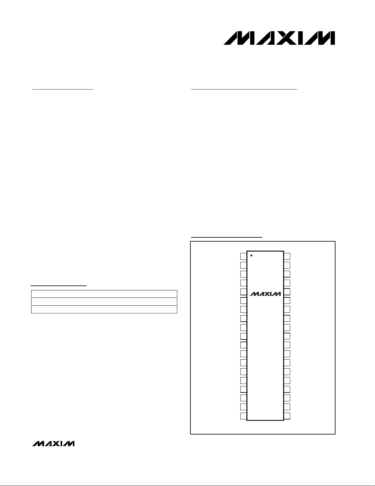
Pin Configuration
TOP VIEW
R3OUT
R2OUT
R1OUT
T3IN
T2IN
T1IN
V
STBY
V
C1+
T4IN
T5IN
T6IN
R6OUT
R7OUT
2 R4INR4OUT
3
4
5
MAX3209E
6
7
8
9
10
DD
11
12
13
14
15
16
TSSOP
381 R5INR5OUT
37
36
R3IN
35
R2IN
34
R1IN
33
T3OUT
T2OUT
32
T1OUT
31
V-
30
C1-
29
GND
28
T4OUT
27
T5OUT
26
T6OUT
25
24
R6IN
R7IN
23
2217 R8INR8OUT
2118 R9INR9OUT
2019 R10INR10OUT

MAX3209E
±15kV ESD-Protected, 12V, Dual RS-232 Serial Port
with Low-Power Standby for Motherboards/Desktops
2 _______________________________________________________________________________________
ABSOLUTE MAXIMUM RATINGS
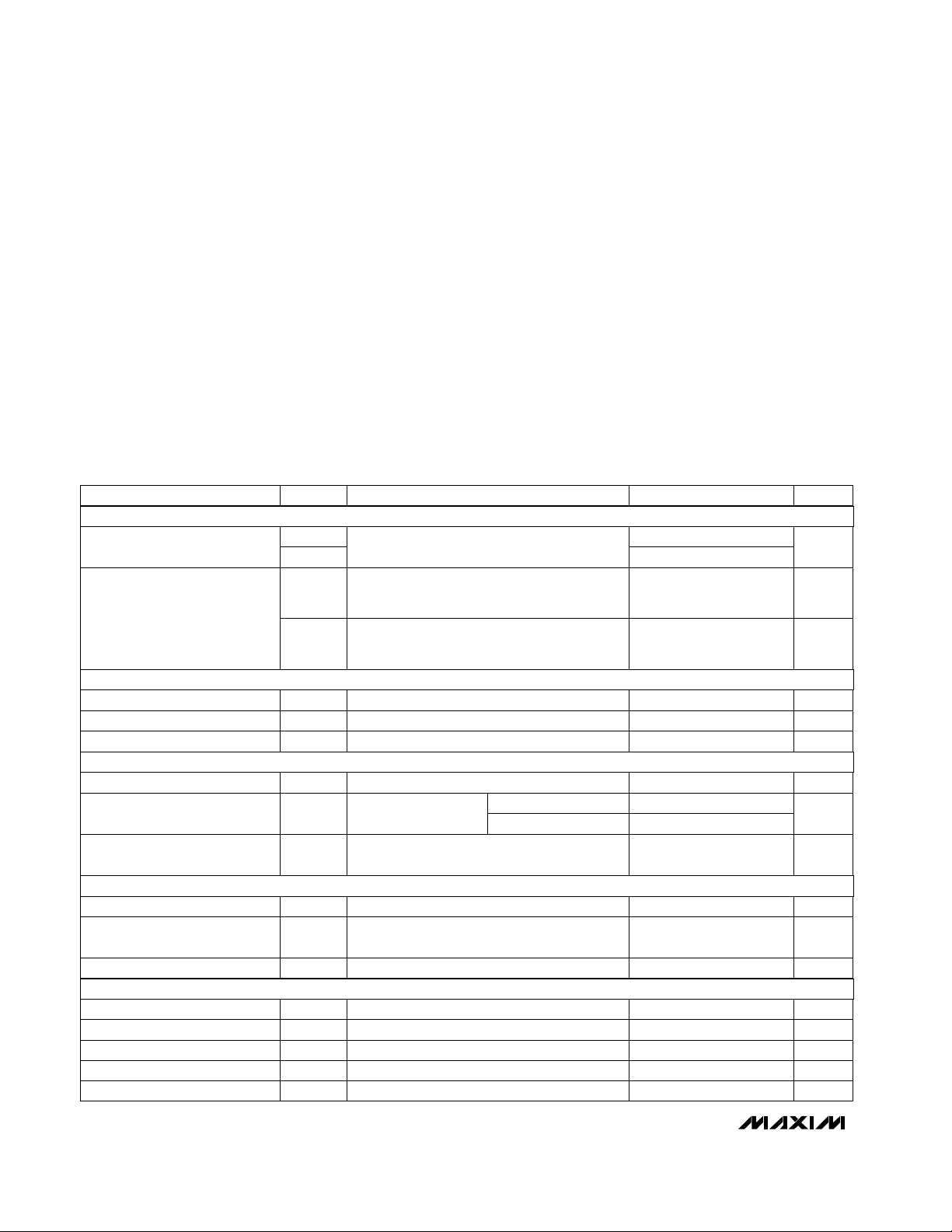
ELECTRICAL CHARACTERISTICS
(VDD= +10.8V to +13.2V, V
STBY
= +3V to +5.5V, C1 = C2 = 0.1µF, TA= T
MIN
to T
MAX
, unless otherwise noted. Typical values are at
T
A
= +25°C, VDD= +12V, V
STBY
= +3.3V.)
Stresses beyond those listed under “Absolute Maximum Ratings” may cause permanent damage to the device. These are stress ratings only, and functional
operation of the device at these or any other conditions beyond those indicated in the operational sections of the specifications is not implied. Exposure to
absolute maximum rating conditions for extended periods may affect device reliability.
VDD.........................................................................-0.3V to +15V
V
STBY
....................................................................... -0.3V to +7V
V- ........................................................................... +0.3V to -15V
Input Voltages
T_IN ......................................................................-0.3V to +7V
R_IN .................................................................................±30V
Output Voltages
T_OUT..............................................................................±15V
R_OUT.................................................-0.3V to (V
STBY
+ 0.3V)
Short-Circuit Duration
T_OUT (one at a time)............................................Continuous
R_OUT (one at a time)............................................Continuous
Continuous Power Dissipation (T
A
= +70°C)
TSSOP (derate 11.8mW/°C above +70°C) ..................941mW
Operating Temperature Ranges
MAX3209EC_ _ ...................................................0°C to +70°C
MAX3209EE_ _ ................................................-40°C to +85°C
Storage Temperature Range ............................-65°C to +150°C
Lead Temperature (soldering, 10sec) ............................+300°C
TA= +25°C
VDD= V
STBY
= 0, V
OUT
= ±2V
V
T_OUT
= 0
Transmitter input at GND
T_IN
All transmitter outputs loaded with 3kΩ to GND
T_IN
VDD= +12V, no load, all transmitter inputs at
V
STBY
, all receiver inputs at V
STBY
or uncon-
nected
R_OUT
CONDITIONS
V2.4RS-232 Input Threshold High
V0.4RS-232 Input Threshold Low
V-25 25Receiver Input Voltage Range
Ω300Transmitter Output Resistance
mA±10 ±60
RS-232 Output Short-Circuit
Current
VOutput Voltage Swing ±5.0
V
V
STBY
- 0.3
V
OHR
Output Voltage High
10.8 13.2V
DD
µA25Input Pull-Up Current
V2V
IHT
Input Logic Threshold High
V0.8V
ILT
Input Logic Threshold Low
3 5.5STBY
0.5 1I
DD
mA
Supply Current
UNITSMIN TYP MAXSYMBOLPARAMETER
V
STBY
= 3.3V V0.2 1RS-232 Input Hysteresis
TA= +25°C kΩ357RS-232 Input Resistance
TA= +25°C
Operating Voltage Range V
VDD= 0, V
STBY
= +3.3V, no load, all transmit-
ter inputs at V
STBY
, all receiver inputs at V
STBY
or unconnected
50 100I
STBY
µA
R_OUT; I
SINK
= 1.6mA V0.4V
OLR
Output Voltage Low
VDD= 0, V
STBY
= 5V µA0.05 ±5
Receiver Output Leakage
Current
V
STBY
- 0.6
I
SOURCE
= 40µA
I
SOURCE
= 1mA
RS-232 RECEIVER INPUTS
RS-232 TRANSMITTER OUTPUTS
TRANSMITTER LOGIC INPUTS
DC CHARACTERISTICS
RECEIVER LOGIC OUTPUTS

MAX3209E
±15kV ESD-Protected, 12V, Dual RS-232 Serial Port
with Low-Power Standby for Motherboards/Desktops
_______________________________________________________________________________________ 3
ELECTRICAL CHARACTERISTICS (continued)
(VDD= +10.8V to +13.2V, V
STBY
= +3V to +5.5V, C1 = C2 = 0.1µF, TA= T
MIN
to T
MAX
, unless otherwise noted. Typical values are at
T
A
= +25°C, VDD= +12V, V
STBY
= +3.3V.)
CL= 1000pF
IEC 1000-4-2 (Contact Discharge)
1
Human Body Model
t
PHLT
µs
SR
Transmitter Output Propagation
Delay, High to Low
V/µsTransmitter Output Slew Rate
IEC 1000-4-2 (Air-Gap Discharge)
CL= 150pF 0.4 1
CONDITIONS
t
PHLR
µs
RL= 3kΩ to 7kΩ, CL= 50pF to 1000pF,
two transmitters switching
Receiver Output Propagation
Delay, High to Low
460DR kbpsGuaranteed Data Rate
±8
±15
61230
RL= 3kΩ to 7kΩ, V
STBY
= 3.3V,
CL= 50pF to 1000pF, TA= +25°C,
measured from +3V to -3V or -3V to +3V
kV
±15
ESD Protection
UNITSMIN TYP MAXSYMBOLPARAMETER
CL= 1000pF 1t
PLHT
µs
Transmitter Output Propagation
Delay, Low to High
T1IN = T2IN = GND, T3IN = V
CC,
T3OUT loaded with 3kΩ to GND, T1OUT and
T2OUT loaded with 2.5mA each
+6 -5 VMouse Driveability
CL= 150pF 0.4 1t
PLHR
µs
Receiver Output Propagation
Delay, Low to High
ESD CHARACTERISTICS
TRANSMITTER TIMING CHARACTERISTICS (Figure 1)
RECEIVER TIMING CHARACTERISTICS
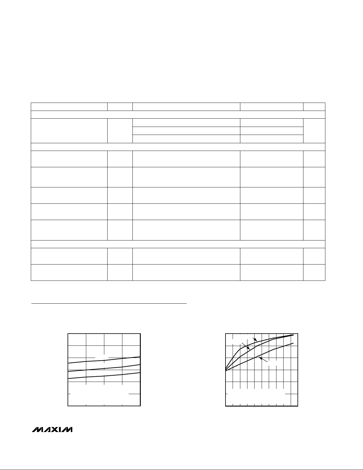
Typical Operating Characteristics
(V
STBY
= +5V, VDD= +12V, C1 = C2 = 0.1µF, TA = +25°C, unless otherwise noted.)
0
15
10
5
20
25
30
0 20001000 3000 4000 5000
SUPPLY CURRENT
vs. LOAD CAPACITANCE
MAX3209E-02
LOAD CAPACITANCE (pF)
SUPPLY CURRENT (mA)
120kbps
240kbps
460kbps
2 TRANSMITTERS AT DATA RATE
4 TRANSMITTERS AT 1/16 DATA RATE
3kΩ + C
L
5
15
10
25
20
30
35
10.8 12.011.4 12.6 13.2
SUPPLY CURRENT vs. SUPPLY VOLTAGE
MAX3209E-01
SUPPLY VOLTAGE (V)
SUPPLY CURRENT (mA)
460kbps
240kbps
120kbps
C1 = C2 = 0.1µF
2 TRANSMITTERS AT DATA RATE
4 TRANSMITTERS AT 1/16 DATA RATE
ALL TRANSMITTERS AT 3kΩ + 1000pF
 Loading...