

For pricing, delivery, and ordering information, please contact Maxim Direct at 1-888-629-4642,
or visit Maxim's website at www.maxim-ic.com.
General Description
The MAX3202E/MAX3203E/MAX3204E/MAX3206E are
low-capacitance ±15kV ESD-protection diode arrays
designed to protect sensitive electronics attached to
communication lines. Each channel consists of a pair of
diodes that steer ESD current pulses to V
CC
or GND.
The MAX3202E/MAX3203E/MAX3204E/MAX3206E protect against ESD pulses up to ±15kV Human Body
Model, ±8kV Contact Discharge, and ±15kV Air-Gap
Discharge, as specified in IEC 61000-4-2. These
devices have a 5pF capacitance per channel, making
them ideal for use on high-speed data I/O interfaces.
The MAX3202E is a two-channel device intended for USB
and USB 2.0 applications. The MAX3203E is a triple-ESD
structure intended for USB On-the-Go (OTG) and video
applications. The MAX3204E is a quad-ESD structure
designed for Ethernet and FireWire
®
applications, and
the MAX3206E is a six-channel device designed for
cell phone connectors and SVGA video connections.
All devices are available in tiny 4-bump (1.05mm x
1.05mm) WLP, 6-bump (1.05mm x 1.57mm) WLP,
9-bump (1.52mm x 1.52mm) WLP, 6-pin (3mm x 3mm)
TDFN, and 12-pin (4mm x 4mm) TQFN packages and
are specified for -40°C to +85°C operation.
Applications
USB Video
USB 2.0 Cell Phones
Ethernet SVGA Video Connections
FireWire
Features
♦ High-Speed Data Line ESD Protection
±15kV—Human Body Model
±8kV—IEC 61000-4-2, Contact Discharge
±15kV—IEC 61000-4-2, Air-Gap Discharge
♦ Tiny WLP Package Available
♦ Low 5pF Input Capacitance
♦ Low 1nA (max) Leakage Current
♦ Low 1nA Supply Current
♦ +0.9V to +5.5V Supply Voltage Range
♦ 2-, 3-, 4-, or 6-Channel Devices Available
MAX3202E/MAX3203E/MAX3204E/MAX3206E
Low-Capacitance, 2/3/4/6-Channel, ±15kV ESD
Protection Arrays for High-Speed Data Interfaces
________________________________________________________________
Maxim Integrated Products
1
Ordering Information
19-2739; Rev 5; 6/11
*
EP = Exposed pad.
Note: All devices operate over -40°C to +85°C temperature
range.
+
Denotes a lead(Pb)-free/RoHS-compliant package.
PART PIN-PACKAGE TOP MARK
MAX3202EEWS+T
4 WLP +AA
MAX3202EETT+T
6 TDFN-EP* +ADQ
MAX3203EEEWT+T
6 WLP +BG
MAX3203EETT+T 6 TDFN-EP* +ADO
MAX3204EEWT+T 6 WLP +AL
MAX3204EETT+T 6 TDFN-EP* + ADP
MAX3206EEWL+T 9 WLP +AQ
MAX3206EETC+ 12 TQFN-EP* +AACA
Selector Guide
Pin Configurations appear at end of data sheet.
FireWire is a registered trademark of Apple Computer, Inc.
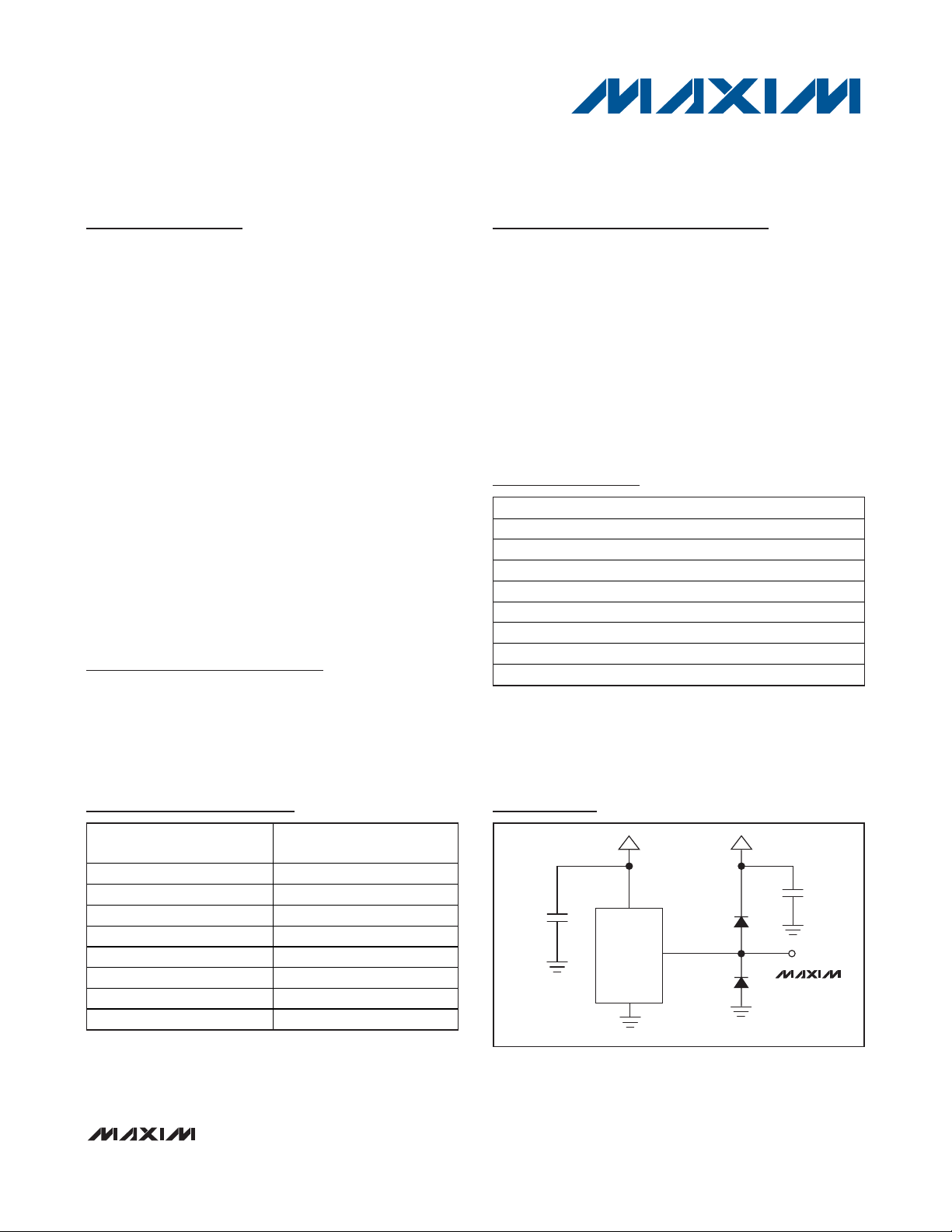
Typical Operating Circuit
PART
MAX3202EEWS+T
MAX3202EETT-T 2
MAX3203EEWT+T 3
MAX3203EETT-T 3
MAX3204EEBT-T 4
MAX3204EETT-T 4
MAX3206EEBL-T 6
MAX3206EETC 6
ESD-PROTECTED
I/O PORTS
2
0.1µF
V
PROTECTED
CIRCUIT
CC
V
CC
0.1µF
I/0_I/0
MAX3202E
MAX3204E
MAX3206E
MAX3208E
MAX3202E/MAX3203E/MAX3204E/MAX3206E
Low-Capacitance, 2/3/4/6-Channel, ±15kV ESD
Protection Arrays for High-Speed Data Interfaces
2 _______________________________________________________________________________________
ABSOLUTE MAXIMUM RATINGS
ELECTRICAL CHARACTERISTICS
(VCC= +5V ±5%, TA= T
MIN
to T
MAX
, unless otherwise noted. Typical values are at VCC= +5V and TA= +25°C.) (Note 2)
Stresses beyond those listed under “Absolute Maximum Ratings” may cause permanent damage to the device. These are stress ratings only, and functional
operation of the device at these or any other conditions beyond those indicated in the operational sections of the specifications is not implied. Exposure to
absolute maximum rating conditions for extended periods may affect device reliability.
Note 2: Limits over temperature are guaranteed by design, not production tested.
Note 3: Idealized clamp voltages (L1 = L2 = L3 = 0) (Figure 1 ); see the
Applications Information
section for more information.
Note 4: Guaranteed by design. Not production tested.
V
CC
to GND...........................................................-0.3V to +7.0V
I/O_ to GND................................................-0.3V to (V
CC
+ 0.3V)
Continuous Power Dissipation (T
A
= +70°C)
2 × 2 WLP (derate 11.5mW/°C above +70°C)...............920mW
3 × 2 WLP (derate 12.3mW/°C above +70°C)...............984mW
3 × 3 WLP (derate 14.1mW/°C above +70°C).............1128mW
6-Pin TDFN (derate 24.4mW/°C above +70°C) ..........1951mW
12-Pin TQFN (derate 16.9mW/°C above +70°C) ........1349mW
Operating Temperature Range ...........................-40°C to +85°C
Storage Temperature Range .............................-65°C to +150°C
Junction Temperature .....................................................+150°C
Lead Temperature (soldering, 10s) .................................+300°C
Soldering Temperature (reflow) .......................................+260°C
Note 1: Package thermal resistances were obtained using the method described in JEDEC specification JESD51-7, using a four-
layer board. For detailed information on package thermal considerations, refer to www.maxim-ic.com/thermal-tutorial
.
PACKAGE THERMAL CHARACTERISTICS (Note 1)
4 WLP
Junction-to-Ambient Thermal Resistance (θ
JA
)...............87°C/W
6 WLP
Junction-to-Ambient Thermal Resistance (θ
JA
)...............84°C/W
9 WLP
Junction-to-Ambient Thermal Resistance (θ
JA
)...............71°C/W
6 TDFN
Junction-to-Ambient Thermal Resistance (θ
JA
)....................42°C/W
Junction-to-Case Thermal Resistance (θ
JC
)...........................9°C/W
12 TQFN
Junction-to-Ambient Thermal Resistance (θ
JA
)....................41°C/W
Junction-to-Case Thermal Resistance (θ
JC
)...........................6°C/W
PARAMETER SYMBOL CONDITIONS MIN TYP MAX UNITS
Supply Voltage V
Supply Current I
Diode Forward Voltage V
Channel Clamp Voltage
(Note 3)
Channel Leakage Current TA = 0°C to +50°C (Note 4) -1 +1 nA
Channel Input Capacitance VCC = 5V, bias of VCC/2 5 7 pF
ESD PROTECTION
Human Body Model ±15 kV
IEC 61000-4-2
Contact Discharge
IEC 61000-4-2
Air-Gap Discharge
CC
CC
IF = 10mA 0.65 0.95 V
F
TA = +25°C, ±15kV
Human Body Model,
I
= 10A
F
TA = +25°C, ±8kV
V
Contact Discharge
C
(IEC 61000-4-2), I
TA = +25°C, ±15kV
Air-Gap Discharge
(IEC 61000-4-2), I
= 24A
F
= 45A
F
0.9 5.5 V
Positive transients V
Negative transients -25
Positive transients V
Negative transients -60
Positive transients V
Negative transients -100
1 100 nA
+ 25
CC
+ 60
CC
+ 100
CC
±8 kV
±15 kV
V
MAX3202E/MAX3203E/MAX3204E/MAX3206E
Low-Capacitance, 2/3/4/6-Channel, ±15kV ESD
Protection Arrays for High-Speed Data Interfaces
_______________________________________________________________________________________
3
Typical Operating Characteristics
(VCC= +5V, TA = +25°C, unless otherwise noted.)
Pin/Bump Description
PIN/BUMP
MAX3202E MAX3203E MAX3204E MAX3206E
WLP
TDFN-
EP
WLP
TDFN-
EP
WLP
TDFN-
EP
WLP
TQFN -
EP
NAME FUNCTION
A1, B2 3, 6
A1,
A2, B3
1, 2, 4
A1, A2,
B2, B3
1, 2, 4,
5
A1, A3,
B1, B3,
C1, C3
1, 2, 3,
7, 8, 9
I/O_ ESD-Protected Channel
A2 4 B1 3 B1 3 A2 5 GND Ground
B1 1 A3 6 A3 6 C2 11 V
CC
Power-Supply Input. Bypass VCC to
GND with a 0.1µF ceramic capacitor.
— 2, 5 — 5 — — —
4, 6,
10, 12
N.C.
No Connection. Not internally
connected.
— — — — — — — — EP
Exposed Pad. Connect to GND. Only
for TDFN and TQFN packages.
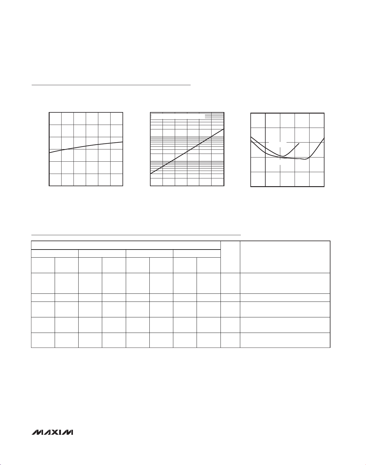
CLAMP VOLTAGE vs. DC CURRENT
1.50
1.30
1.10
0.90
0.70
CLAMP VOLTAGE (V)
0.50
0.30
30 70 9050 110 130 150
DC CURRENT (mA)
1000
MAX3202E toc01
LEAKAGE CURRENT (pA)
LEAKAGE CURRENT vs. TEMPERATURE
LEAKAGE CURRENT PER CHANNEL
100
10
1
25 35
55
45
TEMPERATURE (°C)
65
75 85
INPUT CAPACITANCE vs. INPUT VOLTAGE
12
MAX3202E toc02
10
8
6
INPUT CAPACITANCE (pF)
4
2
021345
VCC = 3.3V
VCC = 5.0V
INPUT VOLTAGE (V)
MAX3202E toc03
Detailed Description
The MAX3202E/MAX3203E/MAX3204E/MAX3206E are
diode arrays designed to protect sensitive electronics
against damage resulting from ESD conditions or transient voltages. The low input capacitance makes these
devices ideal for high-speed data lines. The
MAX3202E, MAX3203E, MAX3204E, and MAX3206E
protect two, three, four, and six channels, respectively.
The MAX3202E/MAX3203E/MAX3204E/MAX3206E are
designed to work in conjunction with a device’s intrinsic
ESD protection. The MAX3202E/MAX3203E/MAX3204E/
MAX3206E limit the excursion of the ESD event to
below ±25V peak voltage when subjected to the
Human Body Model waveform. When subjected to the
IEC 61000-4-2 waveform, the peak voltage is limited to
±60V when subjected to Contact Discharge and ±100V
when subjected to Air-Gap Discharge. The device that
is being protected by the MAX3202E/MAX3203E/
MAX3204E/MAX3206E must be able to withstand these
peak voltages plus any additional voltage generated by
the parasitic board.
Applications Information
Design Considerations
Maximum protection against ESD damage results from
proper board layout (see the
Layout Recommendations
section and Figure 2). A good layout reduces the parasitic series inductance on the ground line, supply line,
and protected signal lines.
The MAX3202E/MAX3203E/MAX3204E/MAX3206E ESD
diodes clamp the voltage on the protected lines during
an ESD event and shunt the current to GND or VCC. In
an ideal circuit, the clamping voltage, VC, is defined as
the forward voltage drop, VF, of the protection diode
plus any supply voltage present on the cathode.
For positive ESD pulses:
VC= VCC+ V
F
For negative ESD pulses:
VC= -V
F
In reality, the effect of the parasitic series inductance
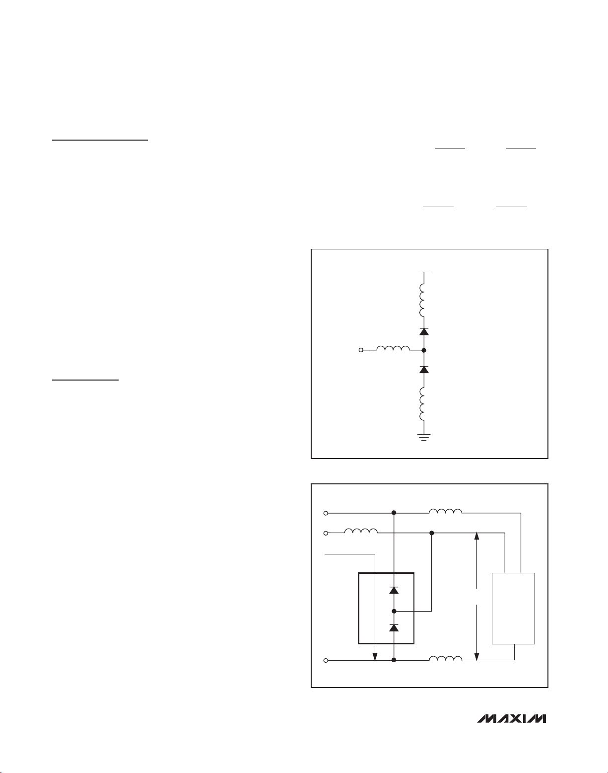
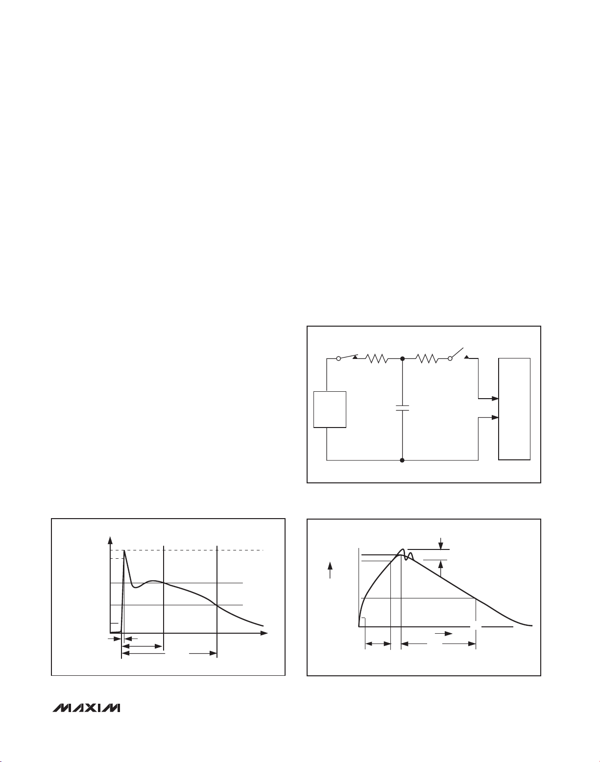
on the lines must also be considered (Figure 1).
For positive ESD pulses:
For negative ESD pulses:
where I
ESD
is the ESD current pulse.
MAX3202E/MAX3203E/MAX3204E/MAX3206E
Low-Capacitance, 2/3/4/6-Channel, ±15kV ESD
Protection Arrays for High-Speed Data Interfaces
4 _______________________________________________________________________________________
Figure 1. Parasitic Series Inductance
Figure 2. Layout Considerations
VV V Lx
=+ +
CCC
FD
1
()
VV Lx
⎛
=− +
C
⎜
FD
()
⎝
⎛
⎜
2
⎝
dI
()
⎞
⎞
⎟
⎠
⎟
⎠
⎛
+
⎜
⎝
⎛
+
L
⎜
⎝
Lx
x
d
⎛
⎜
⎝
13
ESD
12
dt
dI
() (
ESD
dt
POSITIVE SUPPLY RAIL
L2
L1
PROTECTED
LINE
D1
I/O_
D2
D1
D2
L3
GROUND RAIL
I/O_
L2
V
C
PROTECTED
V
CC
L1
PROTECTED LINE
NEGATIVE ESD
CURRENT
PULSE
PATH TO
GROUND
()
dI
ESD
dt
II
)
ESD
dt
CIRCUIT
⎞
⎟
⎠
⎞
⎞
⎟
⎟
⎠
⎠
GND
L3
MAX3202E/MAX3203E/MAX3204E/MAX3206E
Low-Capacitance, 2/3/4/6-Channel, ±15kV ESD
Protection Arrays for High-Speed Data Interfaces
_______________________________________________________________________________________ 5
During an ESD event, the current pulse rises from zero
to peak value in nanoseconds (Figure 3). For example,
in a 15kV IEC-61000 Air-Gap Discharge ESD event,
the pulse current rises to approximately 45A in 1ns
(di/dt = 45 x 10
9
). An inductance of only 10nH adds an
additional 450V to the clamp voltage. An inductance of
10nH represents approximately 0.5in of board trace.
Regardless of the device’s specified diode clamp voltage, a poor layout with parasitic inductance significantly
increases the effective clamp voltage at the protected
signal line.
A low-ESR 0.1µF capacitor must be used between V
CC
and GND. This bypass capacitor absorbs the charge
transferred by an +8kV IEC-61000 Contact Discharge
ESD event.
Ideally, the supply rail (VCC) would absorb the charge
caused by a positive ESD strike without changing its
regulated value. In reality, all power supplies have an
effective output impedance on their positive rails. If a
power supply’s effective output impedance is 1Ω, then
by using V = I × R, the clamping voltage of VCincreases by the equation VC= I
ESD
x R
OUT
. An +8kV IEC
61000-4-2 ESD event generates a current spike of 24A,
so the clamping voltage increases by VC= 24A × 1Ω,
or VC= 24V. Again, a poor layout without proper
bypassing increases the clamping voltage. A ceramic
chip capacitor mounted as close to the MAX3202E/
MAX3203E/MAX3204E/MAX3206E VCCpin is the best
choice for this application. A bypass capacitor should
also be placed as close to the protected device as
possible.
±15kV ESD Protection
ESD protection can be tested in various ways; the
MAX3202E/MAX3203E/MAX3204E/MAX3206E are
characterized for protection to the following limits:
• ±15kV using the Human Body Model
• ±8kV using the Contact Discharge method specified in IEC 61000-4-2
• ±15kV using the IEC 61000-4-2 Air-Gap Discharge
method
ESD Test Conditions
ESD performance depends on a number of conditions.
Contact Maxim for a reliability report that documents
test setup, methodology, and results.
Human Body Model
Figure 4 shows the Human Body Model, and Figure 5
shows the current waveform it generates when discharged into a low impedance. This model consists of
a 100pF capacitor charged to the ESD voltage of interest, which is then discharged into the device through a
1.5kΩ resistor.
Figure 4. Human Body ESD Test Model
Figure 5. Human Body Model Current Waveform
Figure 3. IEC 61000-4-2 ESD Generator Current Waveform
R
D
1.5kΩ
DISCHARGE
RESISTANCE
STORAGE
CAPACITOR
DEVICE
UNDER
TEST
HIGH-
VOLTAGE
DC
SOURCE
R
C
1MΩ
CHARGE-CURRENT-
LIMIT RESISTOR
C
s
100pF
I
100%
90%
PEAK
I
10%
tR = 0.7ns to 1ns
30ns
60ns
t
IP 100%
90%
AMPERES
36.8%
10%
0
0
t
RL
TIME
t
DL
CURRENT WAVEFORM
PEAK-TO-PEAK RINGING
I
r
(NOT DRAWN TO SCALE)
MAX3202E/MAX3203E/MAX3204E/MAX3206E
IEC 61000-4-2
The IEC 61000-4-2 standard covers ESD testing and
performance of finished equipment. The MAX3202E/
MAX3203E/MAX3204E/MAX3206E help users design
equipment that meets Level 4 of IEC 61000-4-2.
The main difference between tests done using the
Human Body Model and IEC 61000-4-2 is higher peak
current in IEC 61000-4-2. Because series resistance is
lower in the IEC 61000-4-2 ESD test model (Figure 6)
the ESD-withstand voltage measured to this standard is
generally lower than that measured using the Human
Body Model. Figure 3 shows the current waveform for
the ±8kV IEC 61000-4-2 Level 4 ESD Contact
Discharge test.
The Air-Gap Discharge test involves approaching the
device with a charged probe. The Contact Discharge
method connects the probe to the device before the
probe is energized.
Layout Recommendations
Proper circuit-board layout is critical to suppress ESDinduced line transients. The MAX3202E/MAX3203E/
MAX3204E/MAX3206E clamp to 100V; however, with
improper layout, the voltage spike at the device is
much higher. A lead inductance of 10nH with a 45A
current spike at a dv/dt of 1ns results in an ADDITION-
AL 450V spike on the protected line. It is essential that
the layout of the PC board follows these guidelines:
1) Minimize trace length between the connector or
input terminal, I/O_, and the protected signal line.
2) Use separate planes for power and ground to reduce
parasitic inductance and to reduce the impedance to
the power rails for shunted ESD current.
3) Ensure short ESD transient return paths to GND
and VCC.
4) Minimize conductive power and ground loops.
5) Do not place critical signals near the edge of the
PC board.
6) Bypass VCCto GND with a low-ESR ceramic capacitor as close to VCCas possible.
7) Bypass the supply of the protected device to GND
with a low-ESR ceramic capacitor as close to the
supply pin as possible.
Low-Capacitance, 2/3/4/6-Channel, ±15kV ESD
Protection Arrays for High-Speed Data Interfaces
6 _______________________________________________________________________________________
Figure 6. IEC 61000-4-2 ESD Test Model
R
C
50Ω to 100Ω
CHARGE-CURRENT-
LIMIT RESISTOR
HIGH-
VOLTAGE
DC
SOURCE
150pF
C
s
R
D
330Ω
DISCHARGE
RESISTANCE
STORAGE
CAPACITOR
DEVICE
UNDER
TEST
MAX3202E/MAX3203E/MAX3204E/MAX3206E
Low-Capacitance, 2/3/4/6-Channel, ±15kV ESD
Protection Arrays for High-Speed Data Interfaces
_______________________________________________________________________________________ 7
Table 1. Reliability Test Data
TEST CONDITIONS DURATION FAILURES PER SAMPLE SIZE
Temperature Cycle
-35°C to +85°C,
-40°C to +100°C
150 cycles,
900 cycles
0/10,
0/200
Operating Life TA = +70°C 240hr 0/10
Moisture Resistance -20°C to +60°C, 90% RH 240hr 0/10
Low-Temperature Storage -20°C 240hr 0/10
Low-Temperature Operational -10°C 24hr 0/10
Solderability 8hr steam age — 0/15
ESD
— 0/5
High-Temperature Operating Life TJ = +150°C 168hr 0/45
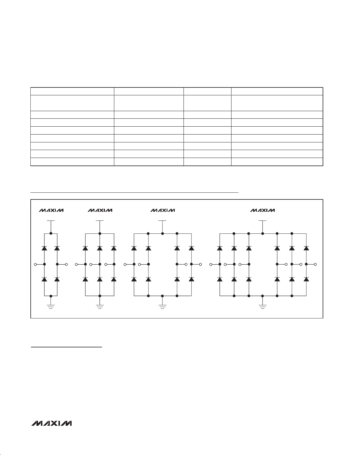
Functional Diagrams
Chip Information
PROCESS: BiCMOS
±2000V, Human Body Model
MAX3202E
V
CC
MAX3203E
V
CC
MAX3204E
V
MAX3206E
CC
V
CC
I/O4
GND
I/O3
I/O1
I/O2
I/O3
I/O1 I/O2
GND
I/O2
I/O1 I/O3
GND
I/O1
I/O2
GND
I/O4
I/O5
I/O6

MAX3202E/MAX3203E/MAX3204E/MAX3206E
Low-Capacitance, 2/3/4/6-Channel, ±15kV ESD
Protection Arrays for High-Speed Data Interfaces
8 _______________________________________________________________________________________
Pin Configurations
PACKAGE TYPE PACKAGE CODE OUTLINE NO.
LAND
PATTERN NO.
4 WLP W41A1+2
21-0455
Refer to Application Note 1891
6 WLP W61C1+2
21-0463
Refer to Application Note 1891
9 WLP W91B1+5
21-0067
Refer to Application Note 1891
6 TDFN-EP T633+2
21-0137
90-0058
12 TQFN-EP T1244+4
21-0139
90-0068
Package Information
For the latest package outline information and land patterns (footprints), go to www.maxim-ic.com/packages. Note that a "+", "#", or
"-" in the package code indicates RoHS status only. Package drawings may show a different suffix character, but the drawing pertains to the package regardless of RoHS status.
TOP VIEW
(BUMPS ON BOTTOM)
GND
I/O2I/O3 V
A2 A3A1
MAX3204E
CC
I/O3
I/O2
A1
B1
A2 A3
MAX3206E
I/O4
I/O5
B3
I/O1
MAX3202E
I/O2I/O3 V
GND
A2A1
CC
A2 A3A1
MAX3203E
V
CC
B1 B2
I/O2
WLP
MAX3202E
+
1
V
CC
2N.C.
EP
3
TDFN
EP = EXPOSED PADDLE. CONNECT TO GND.
6
I/02
5
N.C.
4I/01
GND
B1 B3
GND I/O1
WLP
MAX3203E
B1 B2 B3
I/O4GND I/O1
WLP
MAX3204E
++
6
I/01
1
2I/02
EP EP
3
V
CC
5
N.C.
4GND
I/03
TDFN
I/01
1
2I/02
3
6
5
4GND
TDFN
V
I/04
I/03
C1 C2 C3
I/O1
V
CC
WLP
N.C.11V
CC
12
+
I/01
1
CC
2I/02
3
MAX3206E
EP
45
N.C.
GND6N.C.
TQFN
N.C.
10
9
8
7I/03
I/O6
I/06
I/05
I/04

MAX3202E/MAX3203E/MAX3204E/MAX3206E
Low-Capacitance, 2/3/4/6-Channel, ±15kV ESD
Protection Arrays for High-Speed Data Interfaces
Maxim cannot assume responsibility for use of any circuitry other than circuitry entirely embodied in a Maxim product. No circuit patent licenses are
implied. Maxim reserves the right to change the circuitry and specifications without notice at any time.
Maxim Integrated Products, 120 San Gabriel Drive, Sunnyvale, CA 94086 408-737-7600 _____________________
9
© 2011 Maxim Integrated Products Maxim is a registered trademark of Maxim Integrated Products, Inc.
Revision History
REVISION
NUMBER
3 12/07 Added 3202EEWS+T TDFN and TQFN packages, updated Package Information
4 12/09
5 6/11 Updated to show available packages a s WLP, not UCSP 1, 2, 3, 6, 8
REVISION
DATE
DESCRIPTION
Corrected part numbers and pin pac kages in the Ordering Information table,
Absolute Maximum Ratings, Selector Guide, Pin Description, and Pin
Configurations.
CHANGED
1, 2, 3, 4, 6, 8,
PAGES
12–15
1–3, 8–15
 Loading...