

Page 1
General Description
The MAX3190/MAX3190E single RS-232 transmitters in
a SOT23-6 package are for space- and cost-constrained applications requiring minimal RS-232 communications. These devices consume only 200µA of
supply current from ±7.5V to ±12V supplies. The
MAX3190/MAX3190E transmitter outputs are RS-232
compatible when powered from ±6V to ±7.5V supplies.
They feature a shutdown input that reduces current
consumption to only 1µA and forces the transmitter output into a high-impedance state. RS-232-compliant data
transmission is guaranteed up to 460kbps.
The MAX3190/MAX3190E are EIA/TIA-232 transmitters
that convert CMOS/TTL logic levels to RS-232-compliant
signals. The MAX3190E transmitter output is protected
to ±15kV per the Human Body Model, ±8kV per IEC
1000-4-2 Contact Discharge, and ±15kV per IEC 10004-2 Air-Gap Discharge, providing protection against
harsh environments. The MAX3190/ MAX3190E transmitters have a standard inverting output.
Applications
Set-Top Boxes
Telecommunications
Diagnostic Ports
Networking Equipment
Digital Cameras
Hand-Held Equipment
Features
♦ Small 6-Pin SOT23 Package
♦ ESD-Protected RS-232 Output (MAX3190E)
±15kV per Human Body Model
±8kV per IEC 1000-4-2 Contact Discharge
±15kV per IEC 1000-4-2 Air-Gap Discharge
♦ 200µA Operating Supply Current
♦ Shutdown Reduces Supply Current to 0.4µA
♦ RS-232-Compliant Operation from ±7.5V to ±12V
Supplies
♦ RS-232-Compatible Operations from ±6V to ±7.5V
Supplies
♦ 460kbps Guaranteed Data Rate
♦ Three-State RS-232 Transmitter Output
♦ No External Components
MAX3190/MAX3190E
±15kV ESD-Protected, 460kbps,
RS-232 Transmitters in SOT23-6
________________________________________________________________ Maxim Integrated Products 1
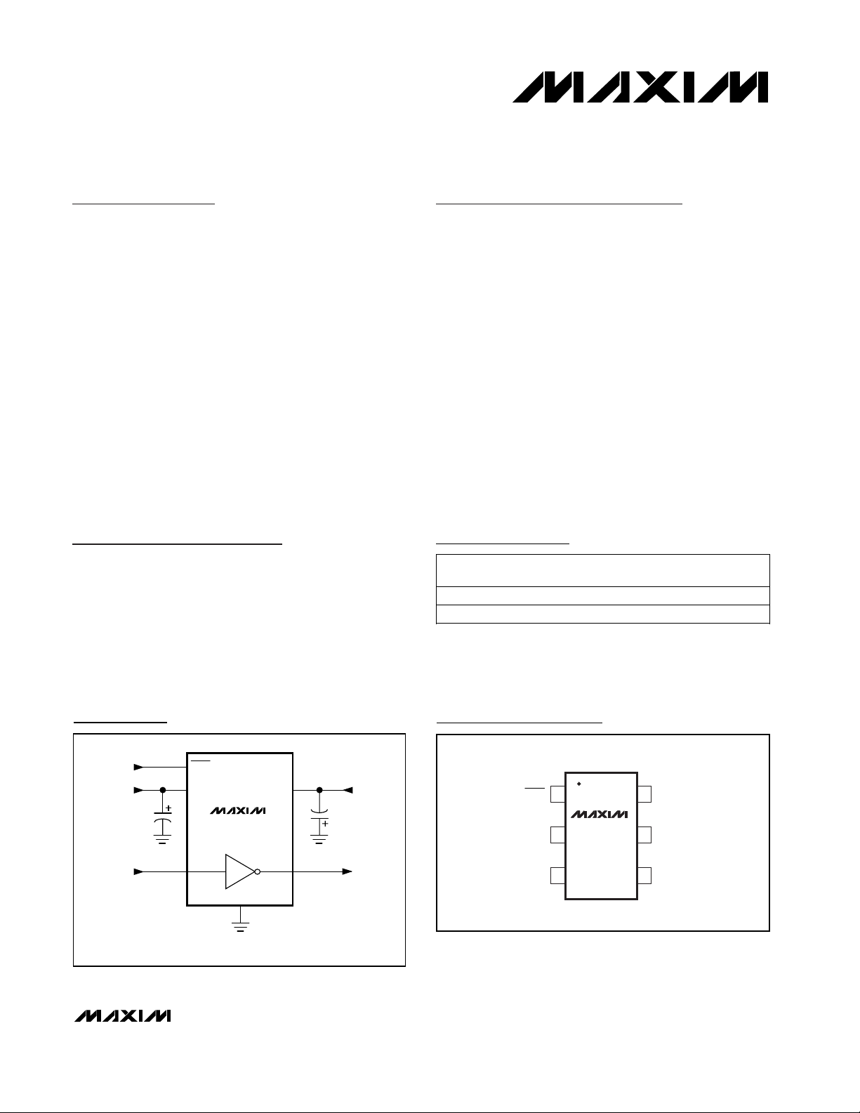
Typical Operating Circuit
19-1931; Rev 1; 3/03
Pin Configuration
Ordering Information
ABQS
AAIA
TOP
MARK
6 SOT23-6
6 SOT23-6
PINPACKAGE
TEMP RANGE
-40°C to +85°C
-40°C to +85°C
MAX3190EEUT-T
MAX3190EUT-T
PART
For pricing, delivery, and ordering information, please contact Maxim/Dallas Direct! at
1-888-629-4642, or visit Maxim’s website at www.maxim-ic.com.
+5V
C
BYPASS1
0.1µF
CAPACITORS MAY BE
POLARIZED OR UNPOLARIZED.
1
SHDN
6
V
CC
TIN
3
MAX3190
MAX3190E
GND
2
V
TOUT
TOP VIEW
5
EE
4
C
BYPASS2
0.1µF
-10V+10V
16V
SHDN
GND
2
34
CC
MAX3190
MAX3190E
SOT23-6
5 V
EE
TOUTTIN
Page 2
MAX3190/MAX3190E
±15kV ESD-Protected, 460kbps,
RS-232 Transmitters in SOT23-6
2 _______________________________________________________________________________________
ABSOLUTE MAXIMUM RATINGS
ELECTRICAL CHARACTERISTICS
(V
CC
= +7.5V to +12V, VEE= -7.5V to -12V, TA= T
MIN
to T
MAX
, unless otherwise noted. Typical values are at V
CC
= +10V,
V
EE
= -10V, and TA= +25°C.) (Note 2)
Stresses beyond those listed under “Absolute Maximum Ratings” may cause permanent damage to the device. These are stress ratings only, and functional
operation of the device at these or any other conditions beyond those indicated in the operational sections of the specifications is not implied. Exposure to
absolute maximum rating conditions for extended periods may affect device reliability.
Note 1: VCCand VEEcan have maximum magnitudes of 13.2V, but their absolute difference cannot exceed 22V.
V
CC
to GND (Note 1)...........................................-0.3V to +13.2V
V
EE
to GND (Note 1)............................................+0.3V to -13.2V
V
CC
to VEE(Note 1) .............................................................+22V
TIN, SHDN to GND ...................................................-0.3V to +7V
TOUT to GND (SHDN = GND)..........................................±13.2V
Output Short-Circuit to GND Duration........................Continuous
Continuous Power Dissipation (T
A
= +70°C)
6-Pin SOT23 (derate 8.7mW/°C above +70°C)..........691mW
Operating Temperature Range ...........................-40°C to +85°C
Junction Temperature......................................................+150°C
Storage Temperature Range .............................-65°C to +150°C
Lead Temperature (soldering, 10s) .................................+300°C
PARAMETER SYMBOL CONDITIONS MIN TYP MAX UNITS
DC CHARACTERISTICS
Positive Supply Voltage V
Negative Supply Voltage V
Positive Supply Current I
Negative Supply Current I
Shutdown Supply Current V
CC
EE
CC
EE
V
SHDN
V
SHDN
SHDN
INPUT LOGIC (TIN, SHDN)
Input Logic Threshold Low V
Input Logic Threshold High V
IL
IH
Input Leakage ±0.01 ±1 µA
TIN Input Hysteresis 100 mV
TRANSMITTER OUTPUT
Output Voltage Swing V
Output Resistance R
TOUT
TOUTVCC
VCC = 7.5V, VEE = -7.5V, RL = 3kΩ ±5 V
VCC = 6V, VEE = -6V, RL = 3kΩ ±3.7 V
Outp ut S hor t- C i r cui t C ur r ent ±35 +60 mA
V
Output Leakage Current I
TOUT
V
TOUT
EE
TIMING CHARACTERISTICS
R
= 3kΩ,
Maximum Data Rate
Transmitter Skew t
Transition-Region Slew Rate
Transmitter Enable Time t
TS
EN
L
= 1000pF
C
L
|t
PHL
= 3kΩ to 7kΩ,
R
L
= 300pF to 1000pF, measured from -3V
C
L
to +3V or +3V to -3V,
V
CC
= +5V 250 µA
= +5V -125 µA
= 0 ±0.4 ±10 µA
= VEE = 0, V
= ±2V 300 Ω
TOUT
= ±12V; VCC = 0 or VCC = +10V,
= -10V; SHDN = GND
- t
|, Figure 1 100 ns
PLH
= +10V, VEE = -10V, TA = +25°C
7.5 12 V
-12 -7.5 V
0.8 V
2.4 V
±100 µA
460 kbps
6 30 V/µs
2µs
Page 3
MAX3190/MAX3190E
±15kV ESD-Protected, 460kbps,
RS-232 Transmitters in SOT23-6
_______________________________________________________________________________________ 3
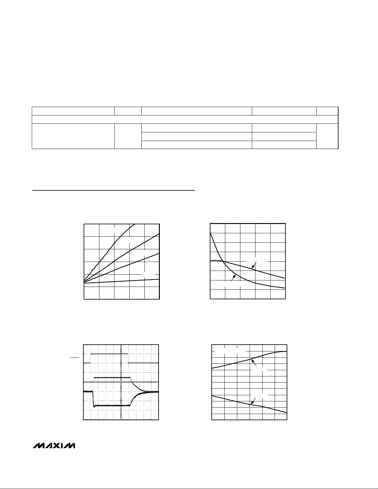
Typical Operating Characteristics
(VCC= +10V, VEE= -10V, RL= 3kΩ, TA= +25°C, unless otherwise noted.)
ELECTRICAL CHARACTERISTICS (continued)
(V
CC
= +7.5V to +12V, VEE= -7.5V to -12V, TA= T
MIN
to T
MAX
, unless otherwise noted. Typical values are at V
CC
= +10V,
V
EE
= -10V, and TA= +25°C.) (Note 2)
Note 2: All devices are 100% tested at T
A
= +25°C. All limits over temperature are guaranteed by design.
PARAMETER SYMBOL CONDITIONS MIN TYP MAX UNITS
ESD PROTECTION (MAX3190E)
Human Body Model ±15
IEC 1000-4-2 Contact Discharge ±8TOUT
IEC 1000-4-2 Air-Gap Discharge ±15
SUPPLY CURRENT
vs. OUTPUT CAPACITANCE
6
5
4
3
2
SUPPLY CURRENT (mA)
1
0
0 500 1000 1500 2000 2500
460kbps
250kbps
125kbps
OUTPUT CAPACITANCE (pF)
20kbps
MAX3190/90E toc01
SLEW RATE (V/µs)
SLEW RATE vs. OUTPUT CAPACITANCE
40
35
30
25
20
15
10
FALLING EDGE
5
0
0 800400 1200 1600 2000
RISING EDGE
CAPACITANCE (pF)
MAX3190/90E toc02
kV
TRANSMITTER OUTPUT
SHUTDOWN WAVEFORM
SHDN
TOUT 0
1.0µs/div
MAX3190/90E toc03
5V
0
+10V
-10V
TRANSMITTER OUTPUT VOLTAGE
vs. SUPPLY VOLTAGE
12
VEE = -VCC, 460kbps
10
8
6
4
2
0
-2
TOUT VOLTAGE (V)
-4
-6
-8
-10
-12
6897 101112
SUPPLY VOLTAGE (V)
POSITIVE
NEGATIVE
MAX3190/90E toc04
Page 4

Detailed Description
The MAX3190/MAX3190E are EIA/TIA-232 transmitters
that convert CMOS/TTL logic levels to RS-232 signals.
They operate on ±7.5V to ±12V supplies and feature
enhanced electrostatic discharge protection (see ESD
Protection). The MAX3190/MAX3190E guarantee a
460kbps data rate with worst-case loads of 3kΩ in parallel with 1000pF. The MAX3190/MAX3190E invert the
TOUT signal relative to TIN (standard RS-232). The
transmitter input does not have a pullup resistor and
should be connected to GND if unused.
Shutdown
The MAX3190/MAX3190E feature a shutdown input.
Drive SHDN low to reduce the supply current to 1µA
(max). Shutdown also forces TOUT into a high-impedance state, allowing the signal line to be safely controlled by other transmitters. Drive SHDN high for
normal operation.
ESD Protection
As with all Maxim devices, ESD protection structures are
incorporated on all pins to protect against ESD encountered during handling and assembly. The MAX3190E’s
transmitter output has extra protection against static
electricity. Maxim has developed state-of-the-art structures enabling this pin to withstand ESD up to ±15kV
without damage or latch-up. The MAX3190E’s transmitter output is characterized for protection to the following
limits:
• ±15kV using the Human Body Model
• ±8kV using the Contact Discharge method specified
in IEC 1000-4-2
• ±15kV using the Air-Gap Discharge method specified
in IEC 1000-4-2
Human Body Model
Figure 2 shows the Human Body Model, and Figure 3
shows the current waveform it generates when discharged into a low impedance. This model consists of
a 100pF capacitor charged to the ESD voltage of interest,
and then discharged into the test device through a
1.5kΩ resistor.
IEC 1000-4-2
The IEC 1000-4-2 standard covers ESD testing and
performance of finished equipment; it does not specifically refer to ICs. The MAX3190E enables the design of
equipment that meets the highest level (Level 4) of IEC
1000-4-2 without the need for additional ESD-protection
components. The major difference between tests done
using the Human Body Model and IEC 1000-4-2 is
higher peak current in IEC 1000-4-2. Because series
resistance is lower in the IEC 1000-4-2 model, the ESD
withstand voltage measured to this standard is generally lower than that measured using the Human Body.
Figure 4 shows the IEC 1000-4-2 model, and Figure 5
MAX3190/MAX3190E
±15kV ESD-Protected, 460kbps,
RS-232 Transmitters in SOT23-6
4 _______________________________________________________________________________________
Pin Description
Figure 1. Transmitter Propagation-Delay Timing
NAME
FUNCTION
1
SHDN
Active-Low Shutdown. Pull low to
reduce the supply current and to force
TOUT into a high-impedance state.
2 GND Ground
PIN
3 TIN TTL/CMOS Transmitter Input
4 TOUT RS-232 Transmitter Output
6 V
CC
Positive Supply Voltage
5 V
EE
Negative Supply Voltage
Figure 2. Human Body ESD Test Model
+10V
TOUT
-10V
t
PLH
t
V
IH
TIN
V
IL
PHL
50%50%
50%50%
R
C
1MΩ
CHARGE-CURRENT
LIMIT RESISTOR
HIGH-
VOLTAGE
DC
SOURCE
100pF
C
s
R
D
1500Ω
DISCHARGE
RESISTANCE
STORAGE
CAPACITOR
DEVICE
UNDER
TEST
Page 5

shows the current waveform for the ±8kV IEC 1000-4-2
Level 4 ESD Contact Discharge test. The Air-Gap test
involves approaching the device with a charged probe.
The Contact Discharge method connects the probe to
the device before the probe is energized.
Power-Supply Decoupling
In most circumstances, 0.1µF bypass capacitors are
adequate for power-supply decoupling. Connect the
bypass capacitors as close to the IC as possible.
Applications Information
Power-Supply Sources
The MAX3190/MAX3190E require ±7.5V to ±12V dual
supplies. For applications where these supply voltages
are not present, a DC-DC converter must be added.
Due to the MAX3190/MAX3190E’s low current consumption, a charge pump can provide the proper supply
voltages and requires a minimal amount of board
space and cost.
When using another RS-232 device containing an internal
unregulated charge pump (Tables 1 and 2), the
MAX3190/MAX3190E may be powered from the internal
charge pump (Figure 6). This eliminates the need for
additional external DC-DC converters to generate the
required ±7.5V to ±12V dual supplies. The MAX3190/
MAX3190E are specifically designed to be used with
Maxim’s RS-232 products listed in Tables 1 and 2.
Competitive RS-232 devices’ charge pumps typically
do not have the capability to power these devices.
The MAX3190/MAX3190E can be operated from ±6V to
±7.5V supplies. In this condition, the devices are guaranteed to be RS-232-compatible (TOUT ≥ +3.7V).
For applications that have ±4.5V to ±6V supplies available, please refer to the MAX3188/MAX3189 or
MAX3188E/MAX3189E data sheet.
MAX3190/MAX3190E
±15kV ESD-Protected, 460kbps,
RS-232 Transmitters in SOT23-6
_______________________________________________________________________________________ 5
Figure 3. Human Body Model Current Waveform
Figure 4. IEC 1000-4-2 ESD Test Model
Figure 5. IEC 1000-4-2 Generator Current Waveform
PEAK-TO-PEAK RINGING
I
r
(NOT DRAWN TO SCALE)
AMPERES
IP 100%
90%
36.8%
10%
0
0
t
RI
TIME
t
DL
CURRENT WAVEFORM
HIGH-
VOLTAGE
DC
SOURCE
R
C
50MΩ TO 100MΩ
CHARGE-CURRENT
LIMIT RESISTOR
C
150pF
s
R
D
330Ω
DISCHARGE
RESISTANCE
STORAGE
CAPACITOR
I
100%
90%
PEAK
I
DEVICE
UNDER
TEST
10%
tR = 0.7ns TO 1ns
30ns
60ns
t
Page 6

MAX3190/MAX3190E
±15kV ESD-Protected, 460kbps,
RS-232 Transmitters in SOT23-6
6 _______________________________________________________________________________________
Figure 6. Powering the MAX3190/MAX3190E
+5V SUPPLY
C
BYPASS
0.1µF
V
CC
C3
0.1µF
C1+
C1
C2
* FOR MAXIM PART NUMBER,
SEE TABLES 1 AND 2.
C1-
C2+
C2-
MAX_ _ _ _*
V+
V-
C4
0.1µF
V
CC
V
EE
MAX3190
MAX3190E
TIN
SHDN
TOUT
GNDGND
+5V
Page 7

MAX3188E/MAX3189E
±15kV ESD-Protected, 460kbps,
RS-232 Transmitters in SOT23-6
_______________________________________________________________________________________ 7
Chip Information
TRANSISTOR COUNT: 75
PROCESS: CMOS
Table 2. ±15kV ESD-Protected RS-232
Devices with Internal Unregulated Charge
Pumps of ±10V (typical)
Table 1. RS-232 Devices with Internal
Unregulated Charge Pumps of ±10V
(typical)
PART NUMBER NO. OF TX/RX
MAX200 5/0 120
MAX201 2/2 120
MAX202 2/2 64
MAX203 2/2 120
MAX204 4/0 120
MAX205 5/5 120
MAX206 4/3 120
MAX207 5/3 120
MAX208 4/4 120
MAX209 3/5 120
MAX211 4/5 120
MAX213 4/5 120
MAX220 2/2 120
MAX221 1/1 250
MAX222 2/2 200
MAX223 4/5 120
MAX225 5/5 120
MAX230 5/0 120
MAX231 2/2 120
MAX232 2/2 120
MAX232A 2/2 200
MAX233A 2/2 200
MAX233 2/2 120
MAX234 4/0 120
MAX235 5/5 120
MAX236 4/3 120
MAX237 5/3 120
MAX238 4/4 120
MAX239 3/5 120
MAX240 5/5 120
MAX241 4/5 120
MAX242 2/2 200
MAX243 2/2 200
MAX244 8/10 120
MAX248 8/8 120
MAX249 6/10 120
DATA RATE
(kbps)
PART NUMBER NO. OF TX/RX
MAX202E 2/2 64
MAX203E 2/2 120
MAX205E 5/5 120
MAX206E 4/3 120
MAX207E 5/3 120
MAX208E 4/4 120
MAX211E 4/5 120
MAX213E 4/5 120
MAX221E 1/1 250
MAX241E 4/5 120
DATA RATE
(kbps)
Page 8

MAX3188E/MAX3189E
±15kV ESD-Protected, 460kbps,
RS-232 Transmitters in SOT23-6
Maxim cannot assume responsibility for use of any circuitry other than circuitry entirely embodied in a Maxim product. No circuit patent licenses are
implied. Maxim reserves the right to change the circuitry and specifications without notice at any time.
8 _____________________Maxim Integrated Products, 120 San Gabriel Drive, Sunnyvale, CA 94086 408-737-7600
© 2003 Maxim Integrated Products Printed USA is a registered trademark of Maxim Integrated Products.
Package Information
(The package drawing(s) in this data sheet may not reflect the most current specifications. For the latest package outline information,
go to www.maxim-ic.com/packages
.)
6LSOT.EPS
 Loading...