

For free samples and the latest literature, visit www.maxim-ic.com or phone 1-800-998-8800.
For small orders, phone 1-800-835-8769.
General Description
The MAX3188/MAX3189 single RS-232 transmitters in a
SOT23-6 package are for space- and cost-constrained
applications requiring minimal RS-232 communications.
These devices consume only 150µA of supply current
from ±4.5V to ±6V supplies. RS-232 data transmission
is guaranteed up to 250kbps with the MAX3188 and up
to 1Mbps with the MAX3189.
The MAX3188/MAX3189 transmitters are inverting level
translators that convert CMOS-logic levels to 5V
EIA/TIA-232 levels. They feature a shutdown input that
reduces current consumption to only 1µA and forces
the transmitter output into a high-impedance state. The
MAX3188/MAX3189 transmitters have a standard
inverting output.
Applications
Diagnostic Ports
Telecommunications
Networking Equipment
Set-Top Boxes
Digital Cameras
Hand-Held Equipment
Features
♦ Small 6-Pin SOT23 Package
♦ 150µA Supply Current
♦ Shutdown Reduces Supply Current to 1µA
♦ Guaranteed Data Rate
1Mbps (MAX3189)
250kbps (MAX3188)
♦ Three-State RS-232 Transmitter Output
♦ No External Components Required
MAX3188/MAX3189
1Mbps, 1µA RS-232 Transmitters in SOT23-6
________________________________________________________________ Maxim Integrated Products 1
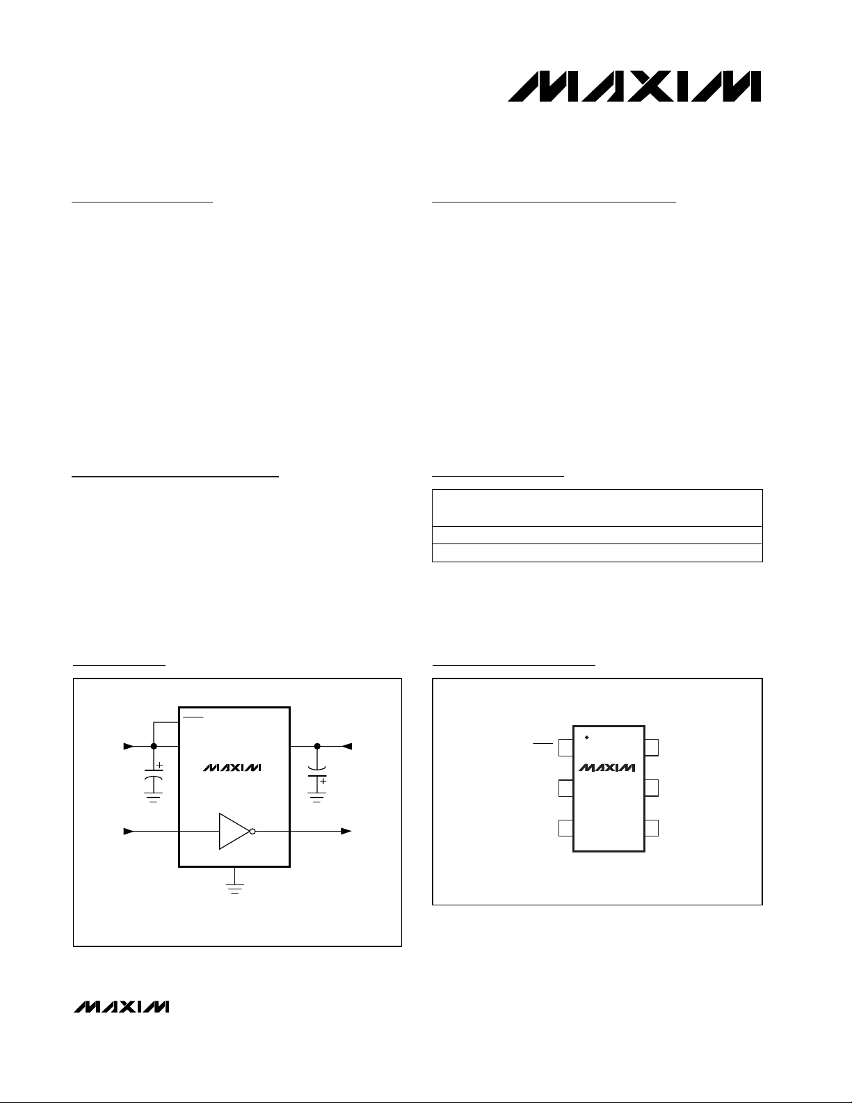
Typical Operating Circuit
19-1628; Rev 0; 2/00
PART
MAX3188EUT-T
MAX3189EUT-T
-40°C to +85°C
-40°C to +85°C
TEMP. RANGE PIN-PACKAGE
6 SOT23-6
6 SOT23-6
Pin Configuration
Ordering Information
TOP
MARK
AAHJ
AAHK
1
SHDN
6
V
CC
C
BYPASS1
0.1µF
TIN
3
CAPACITORS MAY BE
POLARIZED OR UNPOLARIZED.
MAX3188
MAX3189
GND
2
V
TOUT
TOP VIEW
5
EE
4
C
BYPASS2
0.1µF
-5.4V+5.4V
SHDN
GND
16V
MAX3188
2
MAX3189
34
SOT23-6
5 V
CC
EE
TOUTTIN
MAX3188/MAX3189
1Mbps, 1µA RS-232 Transmitters in SOT23-6
2 _______________________________________________________________________________________
ABSOLUTE MAXIMUM RATINGS
ELECTRICAL CHARACTERISTICS
(V
CC
= +4.5V to +6V, VEE= -4.5V to -6V, TA= T
MIN
to T
MAX
, unless otherwise noted. Typical values are at VCC= +5.4V, VEE= -5.4V,
and T
A
= +25°C.) (Note 2)
Stresses beyond those listed under “Absolute Maximum Ratings” may cause permanent damage to the device. These are stress ratings only, and functional
operation of the device at these or any other conditions beyond those indicated in the operational sections of the specifications is not implied. Exposure to
absolute maximum rating conditions for extended periods may affect device reliability.
Note 1: VCCand VEEcan have maximum magnitudes of 7V, but their absolute difference cannot exceed 13V.
Note 2: All devices are 100% tested at T
A
= +25°C. All limits over temperature are guaranteed by design.
V
CC
to GND (Note 1)................................................-0.3V to +7V
V
EE
to GND (Note 1) ................................................+0.3V to –7V
V
CC
to VEE(Note 1) .............................................................+13V
TIN, SHDN to GND ...................................................-0.3V to +7V
TOUT to GND (SHDN = GND)..........................................±13.2V
TOUT to GND (SHDN = V
CC
) ................................................±7V
Output Short-Circuit Duration.....................................Continuous
Continuous Power Dissipation (T
A
= +70°C)
6-Pin SOT23 (derate 8.7mW/°C above +70°C)..........691mW
Operating Temperature Range ...........................-40°C to +85°C
Junction Temperature......................................................+150°C
Storage Temperature Range .............................-65°C to +160°C
Lead Temperature (soldering, 10s) .................................+300°C
MAX3188EUT
MAX3189EUT
MAX3188EUT
MAX3189EUT
MAX3188EUT
RL= 3kΩ to 7kΩ,
C
L
= 150pF to 1000pF,
measured from -3V
to +3V or +3V to -3V,
V
CC
= 5.4V, VEE=
-5.4V, T
A
= +25°C
|t
PHL
- t
PLH
|, Figure 1
RL= 3kΩ,
CL= 1000pF
VCC= VEE= 0, V
TOUT
= ±2V
VCC= 5.4V, VEE= -5.4V, RL= 3kΩ
V
SHDN
= 5V
V
SHDN
= 5V
V
SHDN
= 0
VCC= 4.5V, VEE= -4.5V, RL= 3kΩ
CONDITIONS
24 150
V/µs
630
Transition-Region Slew Rate
25
MAX3189EUT
ns
100
t
TS
Transmitter Skew
1
Mbps
0.25
Maximum Data Rate
µA
±25
I
TOUT
Output Leakage Current
mA
±35 ±60
Output Short-Circuit Current
Ω
300
R
TOUT
Output Resistance
±5
V
±3.7
V
TOUT
Output Voltage Swing
V
-6 -4.5
V
EE
Negative Supply Voltage
V
4.5 6
V
CC
Positive Supply Voltage
mV
100
TIN Input Hysteresis
µA
±0.01 ±1
Input Leakage
V
2.0
V
IH
Input Logic Threshold High
V
0.8
V
IL
Input Logic Threshold Low
µA
110 170
I
CC
Positive Supply Current
µA
45 34
I
EE
Negative Supply Current
µA
0.2 1
Shutdown Supply Current
UNITSMIN TYP MAXSYMBOLPARAMETER
µs
2
t
EN
Transmitter Enable Time
V
OUT
= ±12V; VCC= VEE= 0 or VCC= +5.4V,
V
EE
= -5.4V; SHDN = 0
DC CHARACTERISTICS
INPUT LOGIC (TIN, SHDN)
TRANSMITTER OUTPUTS
TIMING CHARACTERISTICS
MAX3188/MAX3189
1Mbps, 1µA RS-232 Transmitters in SOT23-6
_______________________________________________________________________________________ 3
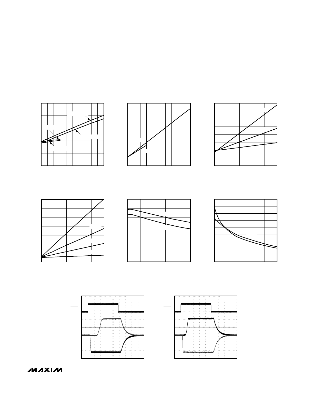
Typical Operating Characteristics
(VCC= +5.4V, VEE= -5.4V, RL= 3kΩ, TA= +25°C, unless otherwise noted.)
SUPPLY CURRENT vs. DATA RATE
= 150pF)
(C
2.5
2.0
ICC (MAX3188)
1.5
1.0
SUPPLY CURRENT (mA)
0.5
0
0 0.40.30.1 0.2 0.5 0.6 0.7 0.8 0.9 1.0
L
ICC (MAX3189)
IEE (MAX3189)
IEE (MAX3188)
DATA RATE (Mbps)
MAX3189
SUPPLY CURRENT
vs. OUTPUT CAPACITANCE
14
12
10
8
6
SUPPLY CURRENT (mA)
4
2
0
0 1000500 1500 2000 2500
OUTPUT CAPACITANCE (pF)
1Mbps
MAX3188/9 toc01
MAX3188/9 toc04
500kbps
240kbps
40kbps
SUPPLY CURRENT vs. DATA RATE
= 1000pF)
(C
7
6
5
4
3
MAX3189
2
SUPPLY CURRENT (mA)
1
0
0 0.40.30.1 0.2 0.5 0.6 0.7 0.8 0.9 1.0
L
MAX3188
DATA RATE (Mbps)
MAX3188
SLEW RATE vs. OUTPUT CAPACITANCE
14
12
10
8
6
SLEW RATE (V/µs)
4
2
0
0 1000500 1500 2000 2500
OUTPUT CAPACITANCE (pF)
-SLEW
+SLEW
4.0
3.5
MAX3188/9 toc02
3.0
2.5
2.0
1.5
SUPPLY CURRENT (mA)
1.0
0.5
MAX3188/9 toc05
SLEW RATE (V/µs)
MAX3188
SUPPLY CURRENT
vs. OUTPUT CAPACITANCE
250kbps
120kbps
40kbps
0
0 500 1000 1500 2000 2500
OUTPUT CAPACITANCE (pF)
MAX3189
SLEW RATE vs. OUTPUT CAPACITANCE
90
80
70
60
50
40
30
20
10
0
0 1000500 1500 2000 2500
OUTPUT CAPACITANCE (pF)
-SLEW
+SLEW
MAX3188/9 toc03
MAX3188/9 toc06
MAX3188
TRANSMITTER OUTPUT
SHUTDOWN WAVEFORM
SHDN
TOUT 0
1µs/div
MAX3188/9 toc07
CL = 150pF
+2V
0
+5V
-5V
SHDN
TOUT 0
MAX3189
TRANSMITTER OUTPUT
SHUTDOWN WAVEFORM
1µs/div
MAX3188/9 toc08
CL = 150pF
+2V
0
+5V
-5V

Detailed Description
The transmitter is an inverting level translator that
converts CMOS-logic levels to 5V EIA/TIA-232 levels.
The MAX3188 guarantees a 250kbps data rate, and the
MAX3189 guarantees a 1Mbps data rate with worst-case
loads of 3kΩ in parallel with 1000pF. The transmitter
input does not have a pull-up resistor and should be
connected to GND if unused.
Shutdown
The MAX3188/MAX3189 feature a shutdown input.
Drive SHDN low to reduce the supply current to 1µA
(max). Shutdown also forces TOUT into a highimpedance state that allows the signal line to be safely
controlled by other transmitters. Drive SHDN high for
normal operation.
Power-Supply Decoupling
In most circumstances, 0.1µF bypass capacitors are
adequate for power-supply decoupling. Connect the
bypass capacitors as close to the IC as possible.
Applications Information
Power-Supply Sources
The MAX3188/MAX3189 require ±4.5V to ±6V dual
supplies. For applications where these supply voltages
are not present, a DC-DC converter must be added.
Due to the devices’ low current consumption, a charge
pump can provide the proper supply voltages and
requires a minimal amount of board space and cost.
When using another RS-232 device containing an internal
regulated charge pump (Table 1), the MAX3188/
MAX3189 may be powered from the internal charge
pump (Figure 2). This eliminates the need for additional
external DC-DC converters to generate the required
±4.5V to ±6V dual supplies.
MAX3188/MAX3189
1Mbps, 1µA RS-232 Transmitters in SOT23-6
4 _______________________________________________________________________________________
Pin Description
Negative Supply VoltageV
EE
5
Positive Supply VoltageV
CC
6
RS-232 Transmitter OutputTOUT4
TTL/CMOS Transmitter InputTIN3
PIN
GroundGND2
Active-Low Shutdown. Pull low to reduce the supply current and to force TOUT into a high-impedance state.
SHDN
1
FUNCTIONNAME
Figure 1. Transmitter Propagation-Delay Timing
+5V
TOUT
-5V
t
PLH
t
V
IH
TIN
V
IL
PHL
50%50%
50%50%

MAX3188/MAX3189
1Mbps, 1µA RS-232 Transmitters in SOT23-6
_______________________________________________________________________________________ 5
PART NO. OF Tx/Rx AutoShutdown™
DATA RATE
(bps)
MAX3224 2/2 250k
MAX3223E 2/2
✓
250k
MAX3223 2/2
✓
120k
MAX3222E 2/2 250k
MAX3224E 2/2 250k
MAX3225 2/2 1M
MAX3225E 2/2 1M
MAX3226 1/1 250k
MAX3221E
MAX3221 1/1
✓
120k
1/1
✓
250k
MAX3222 2/2 120k
MAX3226E 1/1 250k
MAX3227 1/1 1M
MAX3227E 1/1 1M
MAX3232 2/2 120k
MAX3232E 2/2 250k
MAX3237 5/3 1M
MAX3238 5/3 250k
MAX3241 3/5 120k
MAX3241E 3/5 250k
MAX3243 3/5
✓
120k
MAX3243E 3/5
✓
250k
MAX3244 3/5 250k
MAX3244E 3/5 250k
±15kV ESD
PROTECTION
✓
✓
✓
✓
✓
✓
✓
✓
✓
✓
✓
MAX3245 3/5 1M
AutoShutdown
Plus™
✓
✓
✓
✓
✓
✓
✓
✓
✓
✓
✓
✓
MAX3245E 3/5 1M
✓ ✓
Table 1. RS-232 Devices with Internal Regulated Charge Pumps
AutoShutdown and AutoShutdown Plus are trademarks of Maxim Integrated Products.

MAX3188/MAX3189
1Mbps, 1µA RS-232 Transmitters in SOT23-6
6 _______________________________________________________________________________________
Figure 2. Powering the MAX3188/MAX3189
Chip Information
TRANSISTOR COUNT: 111
+3V SUPPLY
C
BYPASS
0.1µF
V
CC
C3
0.1µF
C1
0.1µF
C2
0.1µF
C1+
C1-
C2+
C2-
(TABLE 1)
V+
V-
C4
0.1µF
V
V
TIN
CC
EE
MAX3188
MAX3189
SHDN
TOUT
GNDGND

MAX3188/MAX3189
1Mbps, 1µA RS-232 Transmitters in SOT23-6
_______________________________________________________________________________________ 7
Package Information
6LSOT.EPS

MAX3188/MAX3189
1Mbps, 1µA RS-232 Transmitters in SOT23-6
Maxim cannot assume responsibility for use of any circuitry other than circuitry entirely embodied in a Maxim product. No circuit patent licenses are
implied. Maxim reserves the right to change the circuitry and specifications without notice at any time.
8 _____________________Maxim Integrated Products, 120 San Gabriel Drive, Sunnyvale, CA 94086 408-737-7600
© 2000 Maxim Integrated Products Printed USA is a registered trademark of Maxim Integrated Products.
NOTES
 Loading...