

Page 1
For free samples & the latest literature: http://www.maxim-ic.com, or phone 1-800-998-8800.
For small orders, phone 1-800-835-8769.
General Description
The MAX3180E–MAX3183E single RS-232 receivers in
a SOT23-5 package are designed for space- and costconstrained applications requiring minimal RS-232
communications. The receiver inputs are protected to
±15kV using IEC 1000-4-2 Air-Gap Discharge, to ±8kV
using IEC 1000-4-2 Contact Discharge, and to ±15kV
per the Human Body Model, ensuring compliance with
international standards.
The devices minimize power and heat dissipation by
consuming only 0.5µA supply current from a +3.0V to
+5.5V supply, and they guarantee true RS-232 performance up to a 1.5Mbps data rate. The MAX3180E/
MAX3182E feature a three-state TTL/CMOS receiver
output that is controlled by an EN logic input. The
MAX3181E/MAX3183E feature an INVALID output that
indicates valid RS-232 signals at the receiver input for
applications requiring automatic system wake-up. The
MAX3182E/MAX3183E have a noninverting output,
while the MAX3180E/MAX3181E have a standard
inverting output.
Applications
Diagnostic Ports
Telecommunications
Networking Equipment
Set-Top Boxes
Digital Cameras
Hand-Held Equipment
Features
♦ Tiny SOT23-5 Package
♦ ESD-Protected RS-232 Input
±15kV—Human Body Model
±8kV—IEC 1000-4-2, Contact Discharge
±15kV—IEC 1000-4-2, Air-Gap Discharge
♦ 0.5µA Supply Current
♦ 1.5Mbps Guaranteed Data Rate
♦ Meets EIA/TIA-232 and V.28/V.24 Specifications
Down to V
CC
= +3.0V
♦ INVALID Output Indicates Valid RS-232 Signal at
Receiver Input (MAX3181E/MAX3183E)
♦ Three-State TTL/CMOS Receiver Output
(MAX3180E/MAX3182E)
♦ Noninverting RS-232 Output
(MAX3182E/MAX3183E)
MAX3180E–MAX3183E
±15kV ESD-Protected, 0.5µA, +3V to +5.5V,
1.5Mbps RS-232 Receivers in SOT23-5
________________________________________________________________
Maxim Integrated Products
1
19-1479; Rev 1; 7/99
PART
MAX3180EEUK-T
-40°C to +85°C
TEMP. RANGE
PIN-
PACKAGE
5 SOT23-5
Pin Configurations/Functional Diagrams appear at end of
data sheet.
Selector Guide
Ordering Information
TOP
MARK
ACHB
MAX3181EEUK-T
-40°C to +85°C 5 SOT23-5 ACHC
MAX3182EEUK-T
-40°C to +85°C 5 SOT23-5 ACHD
MAX3183EEUK-T
-40°C to +85°C 5 SOT23-5 ACHE
ESD
PROTECTION
(kV)
MAX3180E ±15
PART PACKAGE
SOT23-5
SUPPLY
CURRENT
(µA)
0.5
EN
INPUT
✓
INVALID
OUTPUT
—
INVERTING
ROUT
✓
NON-
INVERTING
ROUT
—
MAX3181E ±15 SOT23-5 0.5 —
✓ ✓
—
MAX3182E ±15 SOT23-5 0.5
✓
— —
✓
MAX3183E ±15 SOT23-5 0.5 —
✓
—
✓
Page 2
MAX3180E–MAX3183E
±15kV ESD-Protected, 0.5µA, +3V to +5.5V,
1.5Mbps RS-232 Receivers in SOT23-5
2 _______________________________________________________________________________________
ABSOLUTE MAXIMUM RATINGS
ELECTRICAL CHARACTERISTICS
(VCC= +3.0V to +5.5V, TA= T
MIN
to T
MAX
, unless otherwise noted. Typical values are at VCC= +5.0V, TA= +25°C.) (Note 1)
Stresses beyond those listed under “Absolute Maximum Ratings” may cause permanent damage to the device. These are stress ratings only, and functional
operation of the device at these or any other conditions beyond those indicated in the operational sections of the specifications is not implied. Exposure to
absolute maximum rating conditions for extended periods may affect device reliability.
VCCto GND..............................................................-0.3V to +6V
RIN to GND..........................................................................±25V
EN, ROUT, INVALID to GND ......................-0.3V to (V
CC
+ 0.3V)
Continuous Power Dissipation (T
A
= +70°C)
SOT23-5 (derate 7.1mW/°C above +70°C)...................571mW
Operating Temperature Range ...........................-40°C to +85°C
Storage Temperature Range .............................-65°C to +150°C
Lead Temperature (soldering, 10sec) .............................+300°C
VCC= 3.3V or 5V, RIN = VCCor GND, no load
Negative threshold
Positive threshold
VCC= 5.0V
VCC= 3.3V
I
SINK
= 1.6mA
VCC= 5.0V
VCC= 3.3V
VCC= 3.3V
VCC= 5.0V
CONDITIONS
kΩ357R
RIN
Input Resistance
V-0.3 0.3V
ITOL
RIN Threshold to INVALID
Output Low
V
-2.7
V
ITOH
2.7
RIN Threshold to INVALID
Output High
mV300V
HYST
Input Hysteresis
V
1.8 2.7
V
ITH
Input Threshold High
1.5 2.4
V
0.8 1.5
V
ITL
Input Threshold Low
0.6 1.2
V-25 25V
RIN
Input Voltage Range
µA0.5 5.0I
CC
Supply Current
V3.0 5.5V
CC
Supply Voltage
V0.4V
IOL
INVALID Output Voltage Low
µA±0.01 ±1.0I
EN
Leakage Current
V0.8V
IL
Logic Threshold Low
2.0
V
2.4
V
IH
Logic Threshold High
UNITSMIN TYP MAXSYMBOLPARAMETER
I
SINK
= 1.6mA
Receiver disabled
V0.4V
OL
Output Voltage Low
µA±0.05 ±10I
ROUT
Output Leakage Current
I
SOURCE
= 1.0mA V
VCC- VCC-
0.6 0.1
V
OH
Output Voltage High
I
SOURCE
= 1.0mA V
VCC-
0.6
V
IOH
INVALID Output Voltage High
DC CHARACTERISTICS
LOGIC INPUT (EN)
LOGIC OUTPUT
RECEIVER INPUT
RECEIVER OUTPUT
Page 3
MAX3180E–MAX3183E
±15kV ESD-Protected, 0.5µA, +3V to +5.5V,
1.5Mbps RS-232 Receivers in SOT23-5
_______________________________________________________________________________________ 3
ELECTRICAL CHARACTERISTICS (continued)
(VCC= +3.0V to +5.5V, TA= T
MIN
to T
MAX
, unless otherwise noted. Typical values are at VCC= +5.0V, TA= +25°C.) (Note 1)
CONDITIONS
|
t
PHL
- t
PLH
|
, Figure 1
UNITSMIN TYP MAXSYMBOLPARAMETER
CL= 50pF
ns200t
ROE
Receiver Output Enable Time
ns50t
RS
Receiver Skew
Mbps1.5Maximum Data Rate
ns250t
INVH
Receiver Positive or Negative
Threshold to INVALID High
ns200t
ROD
Receiver Output Disable Time
RIN to ROUT; CL= 150pF µs0.15t
PHL
Receiver Propagation Delay,
High-to-Low
RIN to ROUT; CL= 150pF µs0.15t
PLH
Receiver Propagation Delay,
Low-to-High
µs30t
INVL
Receiver Positive or Negative
Threshold to INVALID Low
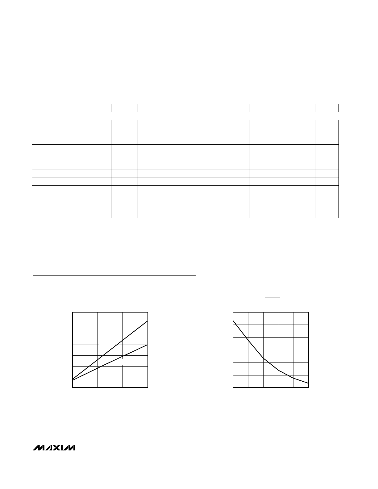
Typical Operating Characteristics
(VCC= +5V, TA= +25°C, unless otherwise noted.)
0
0.2
0.1
0.4
0.3
0.6
0.5
0.7
0 0.5 1.0 1.5
SUPPLY CURRENT vs. DATA RATE
MAX3180E-01
DATA RATE (Mbps)
SUPPLY CURRENT (mA)
R
L
= 50kΩ
C
L
= 100pF
VCC = 5V
VCC = 3.3V
230
270
250
290
330
310
350
3.0 3.5 5.04.54.0 5.5
RIN TO INVALID HIGH
vs. SUPPLY VOLTAGE
MAX3180E-02
VCC (V)
t
INVH
(ns)
TIMING CHARACTERISTICS
Note 1: Specifications are 100% tested at TA= +25°C. Limits over temperature are guaranteed by design.
Page 4

Detailed Description
The MAX3180E–MAX3183E are EIA/TIA-232 and V.28/
V.24 communications receivers that convert RS-232
signals to CMOS logic levels. They operate on a +3V to
+5.5V supply, have 1.5Mbps data rate capability, and
feature enhanced electrostatic discharge (ESD) protection (see
ESD Protection
). All of these devices achieve
a typical supply current of 0.5µA. The MAX3180E/
MAX3182E have a receiver enable control (EN). The
MAX3181E/MAX3183E contain a signal invalid output
(INVALID). The MAX3180E/MAX3181E invert the ROUT
signal relative to RIN (standard RS-232). The
MAX3182E/MAX3183E outputs are not inverted. The
devices come in tiny SOT23-5 packages.
MAX3180E–MAX3183E
±15kV ESD-Protected, 0.5µA, +3V to +5.5V,
1.5Mbps RS-232 Receivers in SOT23-5
4 _______________________________________________________________________________________
25
35
30
45
40
55
50
60
3.0 3.5 4.0 4.5 5.0 5.5
RIN TO INVALID LOW vs. V
CC
MAX3180E-03
VCC (V)
t
INVL
(µs)
50% 50%
50%
0
RIN
5V
ROUT
50%
t
PLH
t
PHL
V
OH
V
OL
Typical Operating Characteristics (continued)
(VCC= +5V, TA= +25°C, unless otherwise noted.)
5V
0
10V
0
-10V
RIN
ROUT
ENABLE
5V
0
500ns/div
MAX3180E
ENABLE ASSERTION TO ROUT RESPONSE
MAX3180E-04
VCC = 5.0V
R
L
= 50kΩ
C
L
= 100pF
1
EN
Receiver Output Enable
Pin Description
NAME
EN
MAX3180E
FUNCTION
MAX3182E
PIN
– Output of the Valid Input Detector
–
2 GND GroundGND
3
ROUT Inverting Receiver Output–
4 RIN Receiver InputRIN
5 V
CC
Supply VoltageV
CC
Figure 1. Receiver Propagation-Delay Timing
– Noninverting Receiver OutputROUT
MAX3181E MAX3183E
–
INVALID
GND
ROUT
–
RIN
V
CC
–
INVALID
GND
–
ROUT
RIN
V
CC
Page 5

Signal Invalid Detector
If no valid signal levels appear on RIN for 30µs (typ),
INVALID goes low. This event typically occurs if the
RS-232 cable is disconnected, or if the connected
peripheral transmitter is turned off. INVALID goes high
when a valid level is applied to the RS-232 receiver
input. Figure 2 shows the input levels and timing diagram for INVALID operation.
Enable Input
The MAX3180E/MAX3182E feature an enable input
(EN). Drive EN high to force ROUT into a high-impedance state. In this state, the devices ignore incoming
RS-232 signals. Pull EN low for normal operation.
ESD Protection
As with all Maxim devices, ESD protection structures
are incorporated on all pins to protect against ESD
encountered during handling and assembly. The
receiver inputs of the MAX3180E–MAX3183E have extra
protection against static electricity. Maxim’s engineers
have developed state-of-the-art structures enabling
these pins to withstand ESD up to ±15kV without damage or latchup. The receiver inputs of the MAX3180E–
MAX3183E are characterized for protection to the following limits:
• ±15kV using the Human Body Model
• ±8kV using the Contact Discharge method specified
in IEC 1000-4-2
• ±15kV using the Air-Gap Discharge method speci-
fied in IEC 1000-4-2
Human Body Model
Figure 3 shows the Human Body Model, and Figure 4
shows the current waveform it generates when discharged into a low impedance. This model consists of
a 100pF capacitor charged to the ESD voltage of interest, and then discharged into the test device through a
1.5kΩ resistor.
MAX3180E–MAX3183E
±15kV ESD-Protected, 0.5µA, +3V to +5.5V,
1.5Mbps RS-232 Receivers in SOT23-5
_______________________________________________________________________________________ 5
CHARGE-CURRENT
LIMIT RESISTOR
DISCHARGE
RESISTANCE
STORAGE
CAPACITOR
C
s
100pF
R
C
1MΩ
R
D
1500Ω
HIGH-
VOLTAGE
DC
SOURCE
DEVICE
UNDER
TEST
Figure 3. Human Body ESD Test Model
IP 100%
90%
36.8%
t
RI
TIME
t
DL
CURRENT WAVEFORM
PEAK-TO-PEAK RINGING
(NOT DRAWN TO SCALE)
I
r
10%
0
0
AMPERES
Figure 4. Human Body Model Current Waveform
VALID SIGNALS
INVALID SIGNALS
VALID SIGNALS
RECEIVER INPUT LEVELS
-2.7V
-0.3V
+2.7V
+0.3V
0
INDETERMINATE
INDETERMINATE
0
V
CC
t
INVL
INVALID
REGION
RECEIVER
INPUT
VOLTAGE
(V)
INVALID
OUTPUT
(V)
t
INVH
Figure 2. Input Levels and INVALID Timing
Page 6

MAX3180E–MAX3183E
IEC 1000-4-2
The IEC 1000-4-2 standard covers ESD testing and
performance of finished equipment; it does not specifically refer to ICs. The MAX3180E–MAX3183E enable the
design of equipment that meets the highest level (Level
4) of IEC 1000-4-2 without the need for additional ESDprotection components.
The major difference between tests done using the
Human Body Model and IEC 1000-4-2 is higher peak
current in IEC 1000-4-2. Because series resistance is
lower in the IEC 1000-4-2 model, the ESD withstand
voltage measured to this standard is generally lower
than that measured using the Human Body. Figure 5
shows the IEC 1000-4-2 model, and Figure 6 shows the
current waveform for the ±8kV IEC 1000-4-2 Level 4
ESD Contact Discharge test.
The Air-Gap test involves approaching the device with
a charged probe. The Contact Discharge method connects the probe to the device before the probe is energized.
Power-Supply Decoupling
In most circumstances, a 0.1µF VCCbypass capacitor
is adequate. Connect the bypass capacitor as close to
the IC as possible.
±15kV ESD-Protected, 0.5µA, +3V to +5.5V,
1.5Mbps RS-232 Receivers in SOT23-5
6 _______________________________________________________________________________________
CHARGE-CURRENT
LIMIT RESISTOR
DISCHARGE
RESISTANCE
STORAGE
CAPACITOR
C
s
150pF
R
C
50MΩ TO 100MΩ
R
D
330Ω
HIGH-
VOLTAGE
DC
SOURCE
DEVICE
UNDER
TEST
Figure 5. IEC 1000-4-2 ESD Test Model
tR= 0.7ns TO 1ns
30ns
60ns
t
100%
90%
10%
I
PEAK
I
Figure 6. IEC 1000-4-2 ESD Generator Current Waveform
Page 7

MAX3180E–MAX3183E
±15kV ESD-Protected, 0.5µA, +3V to +5.5V,
1.5Mbps RS-232 Receivers in SOT23-5
_______________________________________________________________________________________ 7
Pin Configurations/Functional Diagrams
___________________Chip Information
TRANSISTOR COUNT: 41
GND
RINROUT
15
5k
V
CC
( ) ARE FOR MAX3181E/MAX3183E ONLY.
EN (INVALID)
MAX3180E
MAX3181E
SOT23-5
TOP VIEW
2
34
GND
RINROUT
15
5k
V
CC
EN (INVALID)
MAX3182E
MAX3183E
SOT23-5
2
34
Page 8

MAX3180E–MAX3183E
±15kV ESD-Protected, 0.5µA, +3V to +5.5V,
1.5Mbps RS-232 Receivers in SOT23-5
Maxim cannot assume responsibility for use of any circuitry other than circuitry entirely embodied in a Maxim product. No circuit patent licenses are
implied. Maxim reserves the right to change the circuitry and specifications without notice at any time.
8
_____________________Maxim Integrated Products, 120 San Gabriel Drive, Sunnyvale, CA 94086 408-737-7600
© 1999 Maxim Integrated Products Printed USA is a registered trademark of Maxim Integrated Products.
Package Information
SOT5L.EPS
 Loading...