

Page 1
19-6264; Rev 0; 3/12
MAX31826
1-Wire Digital Temperature Sensor
with 1Kb Lockable EEPROM
General Description
The MAX31826 digital thermometer provides 12-bit
temperature measurements and communicates over a
M
1-Wire
bus that by definition requires only one data line
(and ground) for communication with a central microcontroller. It has a -55NC to +125NC operating temperature
range and is accurate to Q0.5NC over the -10NC to +85NC
range. In addition, the device can derive power directly
from the data line (“parasite power”), eliminating the
need for an external power supply.
Each device has a unique 64-bit serial code, which
allows multiple devices to function on the same 1-Wire
bus. Therefore, it is simple to use one microcontroller
(the master device) to control many devices distributed
over a large area. The device includes 128 bytes (1Kb)
of EEPROM for storage of system data. The EEPROM
can be locked to permanently prevent any further data
writes. Four location address inputs simplify mapping of
individual devices to specific locations.
Applications
Industrial Systems
Building Automation
Consumer Equipment
System Calibration
Module Identification
Benefits and Features
S Unique 1-Wire Interface Requires Only One Port
Pin for Communication
S Integrated Temperature Sensor and EEPROM
Reduce Component Count
Measures Temperatures from -55NC to +125NC
(-67NF to +257NF)
±0.5NC Accuracy from -10NC to +85NC
12-Bit Temperature Resolution (0.0625NC)
1Kb EEPROM Can Be Locked to Prevent Further
Writes
S Multidrop Capability Simplifies Multisensor
Systems
Each Device Has a Unique 64-Bit Serial Code
Stored in On-Board ROM
Four Pin-Programmable Bits to Uniquely
Identify Up to 16 Sensor Locations on a Bus
S Can Be Powered from Data Line (3.0V to 3.7V
Power-Supply Range)
S 8-Pin µMAX® Package
Ordering Information appears at end of data sheet.
For related parts and recommended products to use with this part,
refer to www.maxim-ic.com/MAX31826.related.
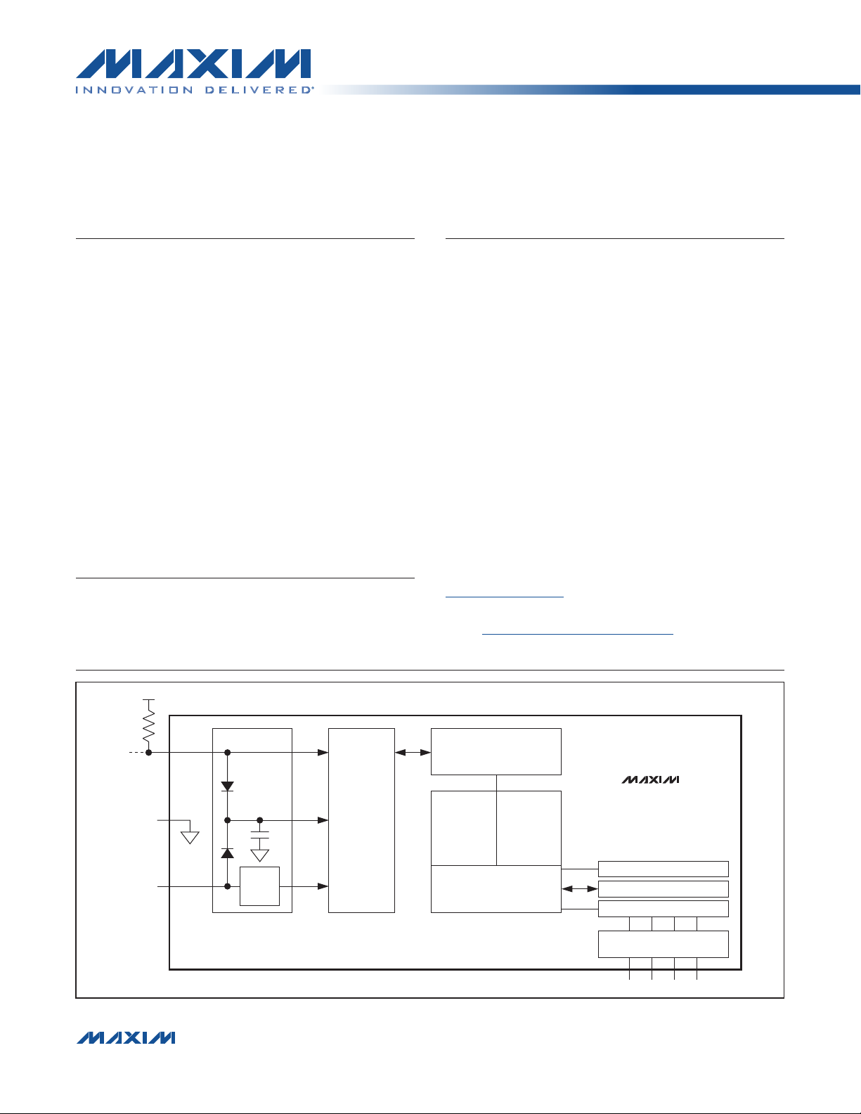
Block Diagram
V
PU
4.7kΩ
MEMORY
DQ
GND
V
DD
1-Wire and µMAX are registered trademarks of Maxim Integrated Products, Inc.
����������������������������������������������������������������� Maxim Integrated Products 1
PARASITE-
POWER
CIRCUIT
POWERSUPPLY
SENSE
64-BIT ROM
AND
C
PP
1-Wire PORT
CONTROL LOGIC
1Kb
EEPROM
SCRATCHPAD 1
MAX31826
SCRATCHPAD 2
16-BIT TEMPERATURE REGISTER
8-BIT CRC GENERATOR
8-BIT CONFIGURATION REGISTER
ADDRESS PIN
INPUT LATCH
AD0 AD1 AD2 AD3
For pricing, delivery, and ordering information, please contact Maxim Direct at 1-888-629-4642,
or visit Maxim’s website at www.maxim-ic.com.
Page 2

MAX31826
1-Wire Digital Temperature Sensor
with 1Kb Lockable EEPROM
ABSOLUTE MAXIMUM RATINGS
Voltage Range on Any Pin Relative to Ground .... -0.5V to +4.5V
Continuous Power Dissipation (TA = +70NC)
FMAX (derate 4.5mW/NC above +70NC) .....................362mW
Operating Temperature Range ........................ -55NC to +125NC
Stresses beyond those listed under “Absolute Maximum Ratings” may cause permanent damage to the device. These are stress ratings only, and functional operation of the device at these or any other conditions beyond those indicated in the operational sections of the specifications is not implied. Exposure to absolute
maximum rating conditions for extended periods may affect device reliability.
DC ELECTRICAL CHARACTERISTICS
(TA = -55°C to +125°C, unless otherwise noted.) (Note 1)
PARAMETER SYMBOL CONDITIONS MIN TYP MAX UNITS
Supply Voltage V
Pullup Supply Voltage
(Notes 2, 3)
Thermometer Error (Note 4) T
Input Logic-Low V
Input Logic-High (Notes 2, 6) V
Sink Current I
Standby Current I
Active Current I
Active Current with
Communication
POR Time t
Input Leakage Current
(AD0–AD3 Pins)
DQ Input Current I
DD
V
PU
ERR
DDS
DD
POR
DQ
Local power (Note 2) +3.0 +3.7 V
Parasite power +3.0 +3.7
Local power +3.0 V
-10NC to +85NC
-55NC to +125NC
(Notes 2, 5) -0.3 +0.8 V
IL
Local power +2.4
IH
Parasite power +3.0
V
L
= 0.4V (Note 2) 4.0 mA
I/O
(Notes 7, 8) 350 1000 nA
VDD = 3.7V (Note 9) 650 1200
Local or parasite power 4 7.8 ms
(Note 10) 5
Storage Temperature Range ............................ -55NC to +125NC
Lead Temperature (soldering, 10s) ................................+300NC
Soldering Temperature (reflow) ......................................+260NC
V
NC
V
FA
FA
FA
FA
-0.5
Q0.25
-2 +2
lower
of 3.7V
(VDD +
0.3V)
lower
of 3.7V
(VDD +
0.3V)
800 1500
-1 +1
DD
+0.5
or
or
����������������������������������������������������������������� Maxim Integrated Products 2
Page 3

MAX31826
1-Wire Digital Temperature Sensor
with 1Kb Lockable EEPROM
AC ELECTRICAL CHARACTERISTICS
(VDD = 3.0V to 3.7V, TA = -55°C to +125°C, unless otherwise noted.) (Note 1)
PARAMETER SYMBOL CONDITIONS MIN TYP MAX UNITS
Temperature Conversion Time t
Time to Strong Pullup On t
Time Slot t
Recovery Time t
Write-Zero Low Time t
Write-One Low Time t
Read Data Valid t
Reset Time High t
Reset Time Low t
Presence-Detect High t
Presence-Detect Low t
DQ Capacitance C
AD0–AD3 Capacitance C
NONVOLATILE MEMORY
EEPROM Write/Erase Cycles N
EEPROM Data Retention t
EEPROM Write Time t
Note 1: Limits are 100% production tested at TA = +25°C and/or TA = +85°C. Limits over the operating temperature range and
relevant supply voltage range are guaranteed by design and characterization. Typical values are not guaranteed.
Note 2: All voltages are referenced to ground.
Note 3: The pullup supply voltage specification assumes that the pullup device is ideal, and therefore the high level of the pullup
is equal to VPU. To meet the device’s VIH specification, the actual supply rail for the strong pullup transistor must include
margin for the voltage drop across the transistor when it is turned on; thus: V
Note 4: Guaranteed by design. These limits represent a three sigma distribution.
Note 5: To guarantee a presence pulse under low-voltage parasite-power conditions, V
as 0.5V.
Note 6: Logic-high voltages are specified at a 1mA source current.
Note 7: Standby current specified up to TA = +70NC. Standby current typically is 3FA at TA = +125NC.
Note 8: To minimize I
Note 9: Active current refers to supply current during active temperature conversions or EEPROM writes.
Note 10: DQ line is high (high-impedance state).
Note 11: See the 1-Wire Timing Diagrams.
Note 12: Under parasite power, if t
, DQ should be within the following ranges: V
DDS
CONV
SPON
SLOT
REC
LOW0
LOW1
RDV
RSTH
RSTL
PDHIGH
PDLOW
IN/OUT
IN_AD
EEWR
EEDR
WR
> 960Fs, a power-on reset (POR) can occur.
RSTL
12-bit resolution 150 ms
Start Convert T command, or Copy
Scratchpad 2 command issued
(Note 11) 60 120
(Note 11) 1
(Note 11) 60 120
(Note 11) 1 15
(Note 11) 15
(Note 11) 480
(Notes 11, 12) 480
(Note 11) 15 60
(Note 11) 60 240
At TA = +25°C
At TA = +85°C (worst case)
At TA = +85°C (worst case)
GND
P VDQ P V
PU_ACTUAL
GND
200k
50k
40 Years
20 25 ms
= V
PU_IDEAL
might need to be reduced to as low
ILMAX
+ 0.3V or VDD - 0.3V P VDQ P VDD.
10
25 pF
50 pF
+ V
TRANSISTOR
Fs
Fs
Fs
Fs
Fs
Fs
Fs
Fs
Fs
Fs
.
����������������������������������������������������������������� Maxim Integrated Products 3
Page 4
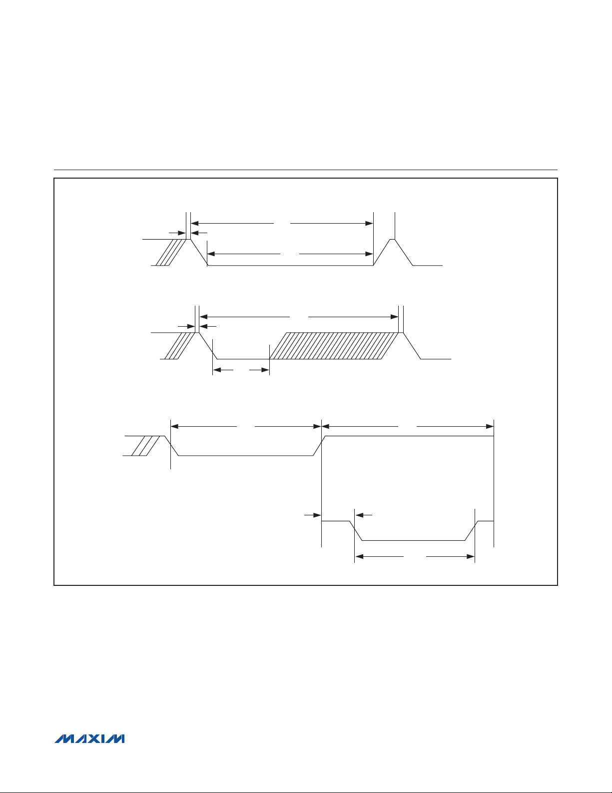
1-Wire WRITE-ZERO TIME SLOT
1-Wire READ-ZERO TIME SLOT
MAX31826
1-Wire Digital Temperature Sensor
with 1Kb Lockable EEPROM
1-Wire Timing Diagrams
t
t
REC
SLOT
t
LOW0
START OF NEXT CYCLE
1-Wire RESET PULSE
1-Wire PRESENCE DETECT
t
REC
t
RDV
RESET PULSE FROM HOST
t
RSTL
t
SLOT
t
PDHIGH
START OF NEXT CYCLE
t
RSTH
PRESENCE DETECT
t
PDLOW
����������������������������������������������������������������� Maxim Integrated Products 4
Page 5
1-Wire Digital Temperature Sensor
(VCC = 3.3V, TA = -40°C, unless otherwise noted.)
THERMOMETER ERROR (˚C)
with 1Kb Lockable EEPROM
Typical Operating Characteristics
MAX31826 TYPICAL ERROR CURVE
0.5
0.4
0.3
0.2
MEAN ERROR
0.1
0
-0.1
-0.2
-0.3
-0.4
-0.5
-40 90
+3s ERROR
-3s ERROR
TEMPERATURE (˚C)
MAX31826
MAX31826 toc01
807050 60-10 0 10 20 30 40-30 -20
TOP VIEW
V
DD
Pin Configuration Pin Description
+
18AD3
27AD2DQ
MAX31826
µMAX
AD1N.C. 36
AD0GND 45
PIN NAME FUNCTION
1 V
Optional VDD. VDD must be grounded for
DD
operation in parasite-power mode.
Data Input/Output. Open-drain 1-Wire
2 DQ
interface pin. Also provides power to
the device when used in parasite-power
mode (see the Parasite Power section.)
3 N.C. No Connection. Not internally connected.
4 GND Ground
5 AD0
Location Address Input (Least Significant
Bit)
6 AD1 Location Address Input
7 AD2 Location Address Input
8 AD3
Location Address Input (Most Significant
Bit)
����������������������������������������������������������������� Maxim Integrated Products 5
Page 6

MAX31826
1-Wire Digital Temperature Sensor
with 1Kb Lockable EEPROM
Detailed Description
The MAX31826 digital thermometer provides 12-bit
temperature measurements and communicates over a
1-WireM bus that by definition requires only one data line
(and ground) for communication with a central microcontroller. The data line requires a weak pullup resistor since
all devices are linked to the bus through a three-state
or open-drain port (i.e., the MAX31826’s DQ pin). Four
location address inputs simplify mapping of individual
devices to specific locations.
Each device has a unique 64-bit serial code, allowing
multiple devices to function on the same 1-Wire bus.
Therefore, it is simple to use one microcontroller to control many devices distributed over a large area. In this
bus system, the microcontroller identifies and addresses
devices on the bus using each device’s unique 64-bit
code. Because each device has a unique code, the
number of devices that can be addressed on one bus
is virtually unlimited. The 1-Wire bus protocol, including
detailed explanations of the commands and time slots, is
described in the 1-Wire Bus System section.
The Scratchpad 1 memory contains the 2-byte temperature register that stores the digital output from the
temperature sensor. An additional 128 bytes (1Kb) of
general-purpose EEPROM is included for storage of system data. The EEPROM can be locked to permanently
prevent any further data writes.
The device can also operate without an external power
supply. Power is instead supplied through the 1-Wire
pullup resistor through DQ when the bus is high. The
high bus signal also charges an internal capacitor (CPP),
which then supplies power to the device when the bus is
low. This method of deriving power from the 1-Wire bus
is referred to as parasite power. Alternatively, a power
supply on VDD can also power the device.
Measuring Temperature
The device’s core functionality is its direct-to-digital temperature sensor. The resolution of the temperature sensor
is 12 bits, corresponding to a least significant bit value
of 0.0625NC. The device powers up in a low-power idle
state. To initiate a temperature measurement, the master
must issue a Convert T command. Following the conversion, the resulting thermal data is stored in the 12-bit temperature register in the Scratchpad 1 memory and the
device returns to its idle state. If the device is powered by
an external supply, the master can issue read time slots
(see the 1-Wire Bus System section) after the Convert T
command, and the device responds by transmitting 0
while the temperature conversion is in progress and 1
when the conversion is done. If the device is powered
with parasite power, this notification technique cannot be
used because the bus must be pulled high by a strong
pullup during the entire temperature conversion. The
bus requirements for parasite power are explained in the
Powering the MAX31826 section.
The temperature data (in NC) is stored as a 16-bit signextended two’s complement number in the temperature
register (see the Temperature Register Format). The sign
bits (S) indicate if the temperature is positive or negative;
for positive numbers S = 0 and for negative numbers
S = 1. Table 1 gives examples of digital output data and
the corresponding temperature readings.
BIT 15 BIT 14 BIT 13 BIT 12 BIT 11 BIT 10 BIT 9 BIT 8
MSB
LSB
1-Wire is a registered trademark of Maxim Integrated Products, Inc.
S S S S S 2
BIT 7 BIT 6 BIT 5 BIT 4 BIT 3 BIT 2 BIT 1 BIT 0
3
2
����������������������������������������������������������������� Maxim Integrated Products 6
2
2
1
2
2
Temperature Register Format
6
0
-1
2
-2
2
5
2
-3
2
4
2
-4
2
Page 7

1-Wire Digital Temperature Sensor
Table 1. Temperature/Data Relationship
MAX31826
with 1Kb Lockable EEPROM
TEMPERATURE (NC)
+125 0000 0111 1101 0000 07D0h
+85 0000 0101 0101 0000 0550h
+25.0625 0000 0001 1001 0001 0191h
+10.125 0000 0000 1010 0010 00A2h
+0.5 0000 0000 0000 1000 0008h
0 0000 0000 0000 0000 0000h
-0.5 1111 1111 1111 1000 FFF8h
-10.125 1111 1111 0101 1110 FF5Eh
-25.0625 1111 1110 0110 1111 FE6Fh
-55 1111 1100 1001 0000 FC90h
DIGITAL OUTPUT (BINARY) DIGITAL OUTPUT (HEX)
Powering the MAX31826
The MAX31826 can be powered by an external supply
on the VDD pin, or it can operate in “parasite power”
mode, which allows the device to function without a local
external supply. Parasite power is useful for applications
that require remote temperature sensing or those that
are very space-constrained. Figure 1 shows the device’s
parasite-power control circuitry, which “steals” power
from the 1-Wire bus through DQ when the bus is high.
The stolen charge powers the device while the bus is
high, and some of the charge is stored on the parasitepower capacitor (CPP) to provide power when the bus is
low. When the device is used in parasite-power mode,
VDD must be connected to ground.
In parasite-power mode, the 1-Wire bus and CPP can provide sufficient current to the device for most operations
as long as the specified timing and voltage requirements
are met (see the DC Electrical Characteristics and the
AC Electrical Characteristics tables). However, when the
device is performing temperature conversions or copying data from the Scratchpad 2 memory to EEPROM, the
operating current can be as high as 1.5mA. This current
can cause an unacceptable voltage drop across the
weak 1-Wire pullup resistor and is more current than can
be supplied by CPP. To ensure that the device has sufficient supply current, it is necessary to provide a strong
pullup on the 1-Wire bus whenever temperature conversions are taking place or when data is being copied from
the Scratchpad 2 to EEPROM. This can be accomplished
by using a MOSFET to pull the bus directly to the rail as
shown in Figure 1. The 1-Wire bus must be switched to
the strong pullup within 10Fs (max) after a Convert T or
Copy Scratchpad 2 command is issued, and the bus
must be held high by the pullup for the duration of the
conversion (t
(tWR). No other activity can take place on the 1-Wire bus
while the pullup is enabled.
The device can also be powered by the conventional
method of connecting an external power supply to VDD,
as shown in Figure 2. The advantage of this method is
that the MOSFET pullup is not required, and the 1-Wire
bus is free to carry other traffic during the temperature
conversion period or EEPROM write time.
The use of parasite power is not recommended for temperatures above 100NC because the device may not be
able to sustain communications due to the higher leakage currents that can exist at these temperatures. For
applications in which such temperatures are likely, it is
strongly recommended that the device be powered by
an external power supply.
In some situations the bus master might not know whether
the devices on the bus are parasite powered or powered
by external supplies. The master needs this information
to determine if the strong bus pullup should be used during temperature conversions. To get this information, the
master can issue a Skip ROM command, followed by a
Read Power Supply command, followed by a read time
slot. During the read time slot, parasite-powered devices
pull the bus low, and externally powered devices let the
bus remain high. If the bus is pulled low, the master
knows that it must supply the strong pullup on the 1-Wire
bus during temperature conversions or EEPROM writes.
) or the duration of the EEPROM write
CONV
����������������������������������������������������������������� Maxim Integrated Products 7
Page 8

MAX31826
1-Wire Digital Temperature Sensor
with 1Kb Lockable EEPROM
V
PU
MAX31826
V
PU
GND DQ V
DD
µP
4.7kΩ
1-Wire BUS
Figure 1. Supplying the Parasite-Powered MAX31826 During Temperature Conversions
MAX31826
V
PU
µP
4.7kΩ
1-Wire BUS
GND DQ V
DD
DD
TO OTHER 1-Wire DEVICES
Figure 2. Powering the MAX31826 with an External Supply
MSb
8-BIT
CRC CODE
MSb MSbLSb
48-BIT SERIAL NUMBER
Figure 3. 64-Bit ROM Code
TO OTHER 1-Wire DEVICES
(EXTERNAL SUPPLY)V
MSbLSb
LSb
8-BIT FAMILY CODE
(3Bh)
LSb
64-Bit ROM Code
Each device contains a unique 64-bit code stored in ROM
(Figure 3). The least significant 8 bits of the ROM code
contain the device’s 1-Wire family code, 3Bh. The next 48
bits contain a unique serial number. The most significant
8 bits contain a cyclic redundancy check (CRC) byte that
����������������������������������������������������������������� Maxim Integrated Products 8
is calculated from the first 56 bits of the ROM code. See
the CRC Generation section for a detailed explanation
of the CRC bits. The 64-bit ROM code and associated
ROM function control logic allow the device to operate as
a 1-Wire device using the protocol detailed in the 1-Wire
Bus System section.
Page 9

1-Wire Digital Temperature Sensor
with 1Kb Lockable EEPROM
SCRATCHPAD 1 (POWER-UP STATE
SHOWN IN PARENTHESES)
TEMPERATURE REGISTER LSB (50h)BYTE 0
TEMPERATURE REGISTER MSB (05h)BYTE 1
RESERVED (FFh)BYTE 2
RESERVED (FFh)BYTE 3
CONFIGURATION REGISTER*BYTE 4
RESERVED (FFh)BYTE 5
RESERVED (FFh)BYTE 6
RESERVED (FFh)BYTE 7
CRCBYTE 8
SCRATCHPAD 2 (EE SCRATCHPAD)
BYTE 0BYTE 0
BYTE 1BYTE 1
......
BYTE 7BYTE 7
*THE LOWER 4 BITS (AD[3:0]) OF THE CONFIGURATION REGISTER ARE HARDWIRED THROUGH AD0–AD3.
EEPROM
BYTES 00h−07h
BYTES 08h−0Fh
BYTES 10h−17h
...
BYTES 70h−77h
BYTES 78h−7Fh
MAX31826
Figure 4. Memory Map
Memory
Scratchpad 2 (the EE scratchpad) is used for writing to
the EEPROM. Scratchpad 2 consists of 8 bytes; write
The device’s memory is organized as shown in Figure 4. The
memory consists of two SRAM scratchpads (Scratchpad 1
and Scratchpad 2) and 1Kb of EEPROM, which can serve
as general-purpose nonvolatile memory until locked.
All memory commands are described in detail in the
MAX31826 Function Commands section.
Byte 0 and byte 1 of Scratchpad 1 contain the least
significant byte and the most significant byte of the temperature register, respectively. Byte 4 contains the configuration information. Bytes 2, 3, 5, 6, and 7 are reserved
for internal use by the device and cannot be overwritten;
these bytes return all ones when read.
Byte 8 of Scratchpad 1 is read-only and contains the
CRC code for bytes 0–7 of the scratchpad. The device
generates this CRC using the method described in the
CRC Generation section.
data to Scratchpad 2 before copying it to the EEPROM.
Configuration Register
Byte 4 of Scratchpad 1 contains the configuration reg-
ister, which is organized as shown in Configuration
Register Format. The configuration register allows the
user to read the programmed value of the address pins.
The AD[3:0] bits report the pin-programmed location
information. Pins connected to DQ (in parasite power)
or VDD (when externally powered) are reported with
logic 1, and pins connected to GND are reported as
logic 0. Pins connected to DQ (in parasite power), VDD
(when externally powered), or GND through a resistor are
valid logic 1s or logic 0s if the resistor is less than 10kI.
Unconnected or high-impedance ( > 10kI) connections
are indeterminate. Bits [7:4] are reserved for internal use
and cannot be overwritten; they return a 1 when read.
Configuration Register Format
BIT 7 BIT 6 BIT 5 BIT 4 BIT 3 BIT 2 BIT 1 BIT 0
— — — — AD3 AD2 AD1 AD0
Note: Bits [3:0] are programmed through the four location programming address pins, AD3–AD0. Reading the configuration register
provides location information on up to 16 individual devices.
����������������������������������������������������������������� Maxim Integrated Products 9
Page 10

MAX31826
1-Wire Digital Temperature Sensor
with 1Kb Lockable EEPROM
CRC Generation
CRC bytes are provided as part of the device’s 64-bit
ROM code, in the 9th byte of Scratchpad 1, and for
Scratchpad 2 values. The ROM code CRC is calculated
from the first 56 bits of the ROM code and is contained in
the most significant byte of the ROM. The two scratchpad
CRCs are calculated from the data in each scratchpad,
and therefore changes when the data in it associated
scratchpad changes. The CRCs provide the bus master with a method of data validation when data is read
from the device. To verify that data has been read correctly, the bus master must recalculate the CRC from
the received data and then compare this value to either
the ROM code CRC (for ROM reads) or to the scratchpads’ CRC (for scratchpad reads). If the calculated CRC
matches the read CRC, the data has been received
error-free. The comparison of CRC values and the decision to continue with an operation are determined entirely
by the bus master. There is no circuitry inside the device
that prevents a command sequence from proceeding if
the device CRC (ROM or scratchpad) does not match the
value generated by the bus master.
The equivalent polynomial function of the CRC (ROM or
scratchpad) is:
CRC = X8 + X5 + X4 + 1
The bus master can recalculate the CRC and compare it
to the CRC values from the device using the polynomial
generator shown in Figure 5. This circuit consists of a
shift register and XOR gates, and the shift register bits
are initialized to 0. Starting with the least significant bit
of the ROM code or the least significant bit of byte 0 in
the scratchpad, one bit at a time should shifted into the
shift register. After shifting in the 56th bit from the ROM
or the most significant bit of byte 7 from the Scratchpad 1
or byte 10 from Scratchpad 2, the polynomial generator
contains the recalculated CRC. Next, the 8-bit ROM code
or scratchpad CRC from the device must be shifted into
the circuit. At this point, if the recalculated CRC was
correct, the shift register contains all zeros. Additional
information about the Maxim 1-Wire CRC is available in
Application Note 27: Understanding and Using Cyclic
Redundancy Checks with Maxim iButton® Products.
1-Wire Bus System
The 1-Wire bus system uses a single bus master to con-
trol one or more slave devices. The MAX31826 is always
a slave. When there is only one slave on the bus, the
system is referred to as a single-drop system; the system
is multidrop if there are multiple slaves on the bus. All
data and commands are transmitted least significant bit
first over the 1-Wire bus.
The following discussion of the 1-Wire bus system is
broken down into three topics: hardware configuration,
transaction sequence, and 1-Wire signaling (signal types
and timing).
Hardware Configuration
The 1-Wire bus has by definition only a single data line.
Each device (master or slave) interfaces to the data line
by using an open-drain or three-state port. This allows
each device to “release” the data line when the device
is not transmitting data so the bus is available for use by
another device. The device’s 1-Wire port (DQ) is open
drain with an internal circuit equivalent to that shown in
Figure 6.
POLYNOMIAL = X8 + X5 + X4 + 1
1ST
STAGE
0
X
Figure 5. CRC Generator
iButton is a registered trademark of Maxim Integrated Products, Inc.
2ND
STAGE
1
X
���������������������������������������������������������������� Maxim Integrated Products 10
3RD
STAGE
2
X
4TH
STAGE
3
X
4
X
5TH
STAGE
6TH
STAGE
5
X
7TH
STAGE
6
X
8TH
STAGE
7
X
INPUT DATA
8
X
Page 11

Rx
BUS MASTER
MAX31826
1-Wire Digital Temperature Sensor
with 1Kb Lockable EEPROM
V
PU
4.7k
Ω
MAX31826 1-Wire PORT
DQ
Rx
Tx
OPEN-DRAIN
PORT PIN
Figure 6. Hardware Configuration
Rx = RECEIVE
Tx = TRANSMIT
The 1-Wire bus requires an external pullup resistor of
approximately 5kI; thus, the idle state for the 1-Wire bus
is high. If for any reason a transaction needs to be suspended, the bus must be left in the idle state if the transaction is to resume. Infinite recovery time can occur between
bits so long as the 1-Wire bus is in the inactive (high) state
during the recovery period. If the bus is held low for more
than 480Fs, all components on the bus are reset.
Transaction Sequence
The transaction sequence for accessing the device is as
follows:
1) Step 1: Initialization
2) Step 2: ROM Command (followed by any required
data exchange)
3) Step 3: MAX31826 Function Command (followed by
any required data exchange)
It is very important to follow this sequence every time the
device is accessed, as the device does not respond if
any steps in the sequence are missing or out of order.
An exception to this rule is the Search ROM command.
After issuing this ROM command, the master must return
to step 1 in the sequence.
Initialization
All transactions on the 1-Wire bus begin with an initialization sequence. The initialization sequence consists of a
reset pulse transmitted by the bus master followed by
presence pulse(s) transmitted by the slave(s). The presence pulse lets the bus master know that slave devices
(such as the MAX31826) are on the bus and are ready
5µA
TYP
100
Ω MOSFET
Tx
to operate. Timing for the reset and presence pulses is
detailed in the 1-Wire Signaling section.
ROM Commands
After the bus master has detected a presence pulse, it
can issue a ROM command. These commands operate
on the unique 64-bit ROM codes of each slave device
and allow the master to single out a specific device if
many are present on the 1-Wire bus. These commands
also allow the master to determine how many and what
types of devices are present on the bus. There are four
ROM commands, and each command is 8 bits long. The
master device must issue an appropriate ROM command
before issuing a MAX31826 function command. Figure 7
shows a flowchart for operation of the ROM commands.
Search ROM [F0h]
When a system is initially powered up, the master must
identify the ROM codes of all slave devices on the
bus, which allows the master to determine the number
of slaves and their device types. The master learns
the ROM codes through a process of elimination that
requires the master to perform a Search ROM cycle (i.e.,
Search ROM command followed by data exchange) as
many times as necessary to identify all the slave devices.
If there is only one slave on the bus, the simpler Read
ROM command can be used in place of the Search ROM
process. For a detailed explanation of the Search ROM
command procedure, refer to Application Note 937: Book
of iButton® Standards. After every Search ROM cycle,
the bus master must return to step 1 (initialization) in the
transaction sequence.
���������������������������������������������������������������� Maxim Integrated Products 11
Page 12

MAX31826
1-Wire Digital Temperature Sensor
with 1Kb Lockable EEPROM
Read ROM [33h]
This command can be used only when there is one slave
on the bus. It allows the bus master to read the slave’s
64-bit ROM code without using the Search ROM command procedure. If this command is used when there is
more than one slave present on the bus, a data collision
occurs when all the slaves attempt to respond at the
same time.
Match ROM [55h]
The Match ROM command followed by a 64-bit ROM
code sequence allows the bus master to address a
specific slave device on a multidrop or single-drop bus.
Only the slave that exactly matches the 64-bit ROM code
sequence responds to the function command issued by
the master; all other slaves on the bus wait for a reset
pulse.
Skip ROM [CCh]
The master can use this command to address all devices
on the bus simultaneously without sending out any ROM
code information. For example, the master can make all
devices on the bus perform simultaneous temperature
conversions by issuing a Skip ROM command followed
by a Convert T function command.
Note that the Read Scratchpad 1 command can follow the
Skip ROM command only if there is a single slave device
on the bus. In this case, time is saved by allowing the
master to read from the slave without sending the device’s
64-bit ROM code. A Skip ROM command followed by a
Read Scratchpad 1 command causes a data collision on
the bus if there is more than one slave because multiple
devices attempt to transmit data simultaneously.
MAX31826 Function Commands
After the bus master has used a ROM command to
address the MAX31826 with which it wishes to communicate, the master can issue one of the MAX31826 function
commands. These commands allow the master to read
from the device’s scratchpad memories, initiate temperature conversions, and determine the power-supply mode.
The MAX31826 function commands are summarized in
Table 2 and illustrated by the flowchart in Figure 8.
Convert T [44h]
This command initiates a single temperature conversion. Following the conversion, the resulting thermal
data is stored in the 2-byte temperature register in the
Scratchpad 1 memory and the device returns to its low-
power idle state. If the device is being used in parasite-
power mode, within 10Fs (max) after this command is
issued, the master must enable a strong pullup on the
1-Wire bus for the duration of the conversion (t
described in the Powering the MAX31826 section. If the
device is powered by an external supply, the master can
issue read time slots after the Convert T command, and
the device responds by transmitting 0 while the tempera-
ture conversion is in progress and 1 when the conversion
is done. In parasite-power mode, this notification tech-
nique cannot be used because the bus is pulled high by
the strong pullup during the conversion.
CONV
) as
Read Scratchpad 1 [BEh]
This command allows the master to read the contents of
Scratchpad 1. The data transfer starts with the least sig-
nificant bit of byte 0 and continues through the scratch-
pad until the 9th byte (byte 8, CRC) is read. The master
can issue a reset to terminate reading at any time if only
part of the scratchpad data is needed. The CRC is com-
puted while data is read from bytes 0–7, and is shifted
out as byte 8.
Read Scratchpad 2 [AAh]
This command allows the master to read the contents of
Scratchpad 2. The command must be issued followed
by the start address to initiate a data transfer. The data
transfer always starts with the least significant bit of the
byte pointed to by the address bits [2:0], and the data
transfer continues through the scratchpad until 8 bytes
have been read. The [2:0] address bits wrap when
address [2:0] = 0x7 to [2:0] = 0x0. The master can issue
a reset to terminate reading at any time if only part of
the scratchpad data is needed. The CRC is computed
dynamically and includes the command, address, and all
the data bytes 0–7 for a total of 10 bytes. The computed
CRC is shifted out at the end of data byte 7. Because
the CRC contains the start address, the CRC value com-
puted can vary with different start addresses.
Note: After the Read Scratchpad 2 command, an address
of 00h returns the scratchpad contents correctly. This is
true regardless of the address sent during a preceding
Write Scratchpad 2 command transaction. However, the
address used during a preceding Write Scratchpad 2
command is necessary here to ensure that future Copy
Scratchpad 2 commands are copied to the correct row.
If 00h is used instead, a future Copy Scratchpad 2 com-
mand copies the contents to address 00h as opposed to
the row addressed by the Write Scratchpad 2 command.
���������������������������������������������������������������� Maxim Integrated Products 12
Page 13

MAX31826
1-Wire Digital Temperature Sensor
with 1Kb Lockable EEPROM
Write Scratchpad 2 [0Fh]
This command allows the master to write 8 bytes to the EE
scratchpad. After issuing the Write Scratchpad 2 command,
the master must first provide the 1-byte address for the first
byte of the target EEPROM page, followed by the 8 bytes of
data to be written to the scratchpad for the EEPROM. The
three lower bits [2:0] of the target address byte must be set
to 0. The device automatically increments the address after
every byte it receives. The device computes the CRC of
the received data, including the command (0Fh), the target
address byte, and the 8 data bytes. After having received
a data byte for address 07h, the device shifts out (back to
the master) the computed CRC of the 10-byte stream just
received, allowing the master to verify that the data was
received correctly. Note that, because the device switches
direction from receive to transmit, writes to Scratchpad 2
must start with address bits [2:0] set to 0 and proceed from
0h–7h and not beyond.
Copy Scratchpad 2 [55h]
This command allows the master to copy the contents of
an 8-byte page of data from Scratchpad 2 to the 1Kb user
memory. The command is followed by the byte A5h. After
the master writes A5h, the device enters the programming
cycle, saving the data to nonvolatile memory, and does not
respond to further communication for the duration of the
EEPROM write time (tWR). During nonparasitic-power mode,
communication with other devices can continue. If the
device is being used in parasite-power mode, within 10Fs
(max) after A5h is issued, the master must enable a strong
pullup on the 1-Wire bus for the duration of the EEPROM
write time (tWR) as described in the Powering the MAX31826
section. No other activity can take place on the 1-Wire bus
while the strong pullup is enabled.
Changing only 1 byte of EEPROM is not natively supported
on the device. To achieve this, the master must first read the
8-byte block that contains the single byte to be changed,
and the three lower bits [2:0] of the target address byte
must be 0. The master must then modify the single byte
and write back the 8 bytes with Write Scratchpad 2 and the
same target address. Finally, the master must issue a Copy
Scratchpad 2 command.
Note: The Copy Scratchpad 2 command uses the more
recent of the two 8-bit addresses provided by either the
Write Scratchpad 2 or Read Scratchpad 2 commands as
the EEPROM destination address. The recommended procedure for writing to EEPROM starting at address 08h is as
follows:
1) Write Scratchpad 2 (address = 08h, 8 data bytes).
2) Read Scratchpad 2 (address = 08h, 8 data bytes). This
reads the data correctly as expected.
3) Copy Scratchpad 2 (0xA5).
4) Data is copied to row 1, which is the correct destination
based on the Write Scratchpad 2 address.
Read Memory [F0h]
This command allows the master to read the contents of the
1Kb memory. The command is followed by the address of
the first byte to be read (00h–7Fh). The data transfer starts
with the least significant bit of the first byte and continues
through 7Fh. The master can issue a reset to terminate reading at any time.
Read Power Supply [B4h]
The master device issues this command followed by a read
time slot to determine if any devices on the bus are using
parasite power. During the read time slot, parasite-powered
devices pull the bus low, and externally powered devices
do not pull the bus low. See the Powering the MAX31826
section for more information.
Lock Low Memory and Lock High Memory
The Lock Low Memory and Lock High Memory routines
each lock the contents of eight pages of memory.
Lock Low Memory (bytes 00h–3Fh) as follows:
1) Initialize communication by issuing a reset and a ROM
command.
2) Send Write Scratchpad 2 command.
3) Send address 80h as the target address to be written.
4) Send data 55h.
5) Initialize and send Copy Scratchpad 2 command.
6) Issue write token A5h and wait tWR.
Locations 00–3Fh are now locked. Also, location 80h is
locked with value 55h. Location 80h cannot be changed to
alter the lock status of 00h–3Fh.
Lock High Memory (bytes 40h–7Fh) as follows:
1) Initialize communication by issuing a reset and a ROM
command.
2) Send Write Scratchpad 2 command.
3) Send address 81h as the target address to be written.
4) Send data 55h.
5) Initialize and send Copy Scratchpad 2 command.
6) Issue write token A5h and wait tWR.
���������������������������������������������������������������� Maxim Integrated Products 13
Page 14

1-Wire Digital Temperature Sensor
with 1Kb Lockable EEPROM
Table 2. MAX31826 Function Command Set
MAX31826
COMMAND DESCRIPTION PROTOCOL
Convert T
(Note 1)
Read Scratchpad 1
(Note 2)
Read Scratchpad 2
(Note 2)
Write Scratchpad 2
(Note 2)
Copy Scratchpad 2
Read Memory
(Note 2)
Read Power Supply
Lock Low Memory
Lock High Memory
Note 1: For parasite-powered devices, the master must enable a strong pullup on the 1-Wire bus during temperature conversions
and copies from the Scratchpad 2 to EEPROM. No other bus activity can take place during this time.
Note 2: The master can interrupt the transmission of data at any time by issuing a reset.
Initiates temperature conversion. 44h
Reads the 9-byte scratchpad
including the CRC byte.
Reads the 9-byte EE scratchpad
including the CRC byte.
Writes to the 8-byte EE
scratchpad.
Writes the contents of the 8-byte
Scratchpad 2 to the EEPROM.
Reads data in the 1Kb user
memory.
Signals the device’s power-supply
mode to the master.
Prevents further changes to the
lower eight pages of user memory.
Prevents further changes to the
upper eight pages of user memory.
BEh
AAh
0Fh
55h
F0h
B4h The device transmits supply status to the master.
—
—
1-Wire BUS ACTIVITY AFTER COMMAND IS
ISSUED
The device transmits conversion status to master
(not applicable for parasite-powered devices).
The device transmits up to 9 data bytes to master.
The 9th byte is the CRC byte.
The master transmits the start address. The device
transmits up to 9 data bytes to the master. The 9th
byte is the CRC byte.
The master transmits the address of first byte in the
target page, and then transmits 8 data bytes. The
device then returns the CRC byte calculated from
the 10 bytes just transmitted.
The master transmits token A5h. The device enters
EEPROM write mode, during which communication
is not allowed in parasitic-power mode.
Additionally, a strong pullup is also required during
parasitic-power mode.
The master transmits the address of first byte to be
read. The device then transmits data starting with
first byte until reaching the end of the available
addresses or until the master issues a reset.
Write 55h to byte 80h of Scratchpad 2. Copy
Scratchpad 2 to EEPROM.
Write 55h to byte 81h of Scratchpad 2. Copy
Scratchpad 2 to EEPROM.
���������������������������������������������������������������� Maxim Integrated Products 14
Page 15

INITIALIZATION
SEQUENCE
MAX31826
1-Wire Digital Temperature Sensor
with 1Kb Lockable EEPROM
MASTER Tx
RESET PULSE
MAX31826 Tx
PRESENCE PULSE
MASTER Tx
ROM COMMAND
33h
READ
ROM?
Y
MAX31826 Tx
FAMILY CODE
1 BYTE
MAX31826 Tx
SERIAL NUMBER
6 BYTES
MAX31826 Tx
CRC BYTE
55h
N
MATCH
ROM?
MASTER Tx
BIT 0
BIT 0
MATCH?
MASTER Tx
BIT 1
BIT 1
MATCH?
MASTER Tx
BIT 63
N
Y Y
Y Y
Y
F0h
SEARCH
ROM?
MAX31826 Tx BIT 0
MAX31826 Tx BIT 0
MASTER Tx BIT 0
BIT 0
NN
MATCH?
MAX31826 Tx BIT 1
MAX31826 Tx BIT 1
MASTER Tx BIT 1
BIT 1
NN
MATCH?
Y
MAX31826 Tx BIT 63
MAX31826 Tx BIT 63
MASTER Tx BIT 63
N
CCh
SKIP
ROM?
N
Y
Figure 7. ROM Commands Flowchart
���������������������������������������������������������������� Maxim Integrated Products 15
BIT 63
MATCH?
Y Y
FUNCTION COMMAND
NN
MASTER Tx
BIT 63
MATCH?
Page 16

MAX31826
1-Wire Digital Temperature Sensor
with 1Kb Lockable EEPROM
MASTER Tx
FUNCTION COMMAND
MAX31826 BEGINS
CONVERSION
DEVICE
CONVERTING
TEMPERATURE?
Y
MASTER Rx
“0s”
B4h
READ
POWER SUPPLY?
N
MASTER Rx
“1s”
44h
CONVERT T?
Y
PARASITE
POWER?
STRONG PULLUP ON DQ
MAX31826 CONVERTS
N
YN
MASTER ENABLES
TEMPERATURE
MASTER DISABLES
STRONG PULLUP
NN
READ
SCRATCHPAD 1?
SCRATCHPAD 2 TO EEPROM
BEh
Y
DATA COPIED FROM
55h
COPY
SCRATCHPAD 2?
MASTER Tx
TOKEN A5h
PARASITE
POWER?
SCRATCHPAD 2 TO EEPROM
N
READ
SCRATCHPAD 2?
N
YN
MASTER ENABLES
STRONG PULLUP ON DQ
DATA COPIED FROM
MASTER DISABLES
STRONG PULLUP
AAh
YY
F0h
READ
MEMORY?
MASTER Tx
START ADDRESS
MASTER Rx DATA BYTE
FROM EEPROM
N
MASTER Tx
RESET?
N
0Fh
WRITE
SCRATCHPAD 2?
N
Y
Y
Y
YN
MASTER Rx
“0s”
MASTER Rx DATA BYTE
FROM SCRATCHPAD 1
N
HAVE 8 BYTES
SCRATCHPAD 1 CRC BYTE
RETURN TO INITIALIZATION SEQUENCE
MASTER Rx
“1s”
PARASITE
POWER?
Figure 8. MAX31826 Function Commands Flowchart
���������������������������������������������������������������� Maxim Integrated Products 16
MASTER Tx
RESET?
N
BEEN READ?
Y
MASTER Rx
FOR NEXT TRANSACTION
MASTER Tx
START ADDRESS
MASTER Rx DATA BYTE
FROM SCRATCHPAD 2
Y
MASTER Tx
RESET?
N
N
HAVE 8 BYTES
BEEN READ?
Y
MASTER Rx
SCRATCHPAD 2 CRC BYTE
Y
MASTER Tx EEPROM
PAGE ADDRESS
MASTER Tx 8 DATA
BYTES
MASTER Rx
CRC BYTE
Page 17

MAX31826
1-Wire Digital Temperature Sensor
with 1Kb Lockable EEPROM
SEARCH ALL
ROM IDs ON BUS
AND
STORE ROM IDs
(F0h COMMAND)
BUILDING CROSS-REFERENCE TABLE
USING ROM IDs AND 4-BIT ADDRESSES
INCREMENT COUNTER
N = N + 1
Figure 9. Building a Cross-Reference Table
N > N
MASTER Tx
NEXT ROM ID
READ SCRATCHPAD 1
(USE AD3−AD0 FROM
CONFIG REGISTER)
MATCH ROM ID TO
ADDRESS AND ADD TO
CROSS-REFERENCE
TABLE
Y
?
MAX
N
MAX
OF ROM IDs FOUND
N
IS THE NUMBER
Locations 40h–7Fh are now locked. Also, location 81h is
locked with value 55h. Location 81h cannot be changed to
alter the lock status of 40h–7Fh.
Building a Cross-Reference Table
The procedure in Figure 9 uses the Search ROM command to find all MAX31826s on the 1-Wire bus (16
maximum) and then reads each configuration register to
match the ROM IDs to the hardwired addresses.
1-Wire Signaling
The device uses a strict 1-Wire communication protocol
to ensure data integrity. Several signal types are defined
by this protocol: reset pulse, presence pulse, write-zero,
write-one, read-zero, and read-one. The bus master initiates all these signals except the presence pulse.
DONE
CROSS-REFERENCE TABLE
ROM ID AD3−AD0
ROM ID(0) 0000
ROM ID(1)
ROM ID(2) 0010
ROM ID(3) 0011
ROM ID(12) 1100
ROM ID(13) 1101
ROM ID(14) 1110
ROM ID(15) 1111
NOTE: TEMPERATURE SENSORS ARE ADDRESSED
BY ROM ID, NOT BY BINARY ADDRESS.
0001
Initialization Procedure:
Reset and Presence Pulses
All communication with the device begins with an initialization sequence that consists of a reset pulse from the
master followed by a presence pulse from the device.
This is illustrated in Figure 10. When the device sends the
presence pulse in response to the reset, it is indicating
to the master that it is on the bus and ready to operate.
During the initialization sequence, the bus master transmits (Tx) the reset pulse by pulling the 1-Wire bus low for
480Fs (min). The bus master then releases the bus and
goes into receive mode (Rx). When the bus is released,
the 5kI pullup resistor pulls the 1-Wire bus high. When
the device detects this rising edge, it waits 15Fs to 60Fs
and then transmits a presence pulse by pulling the
1-Wire bus low for 60Fs to 240Fs.
���������������������������������������������������������������� Maxim Integrated Products 17
Page 18

MAX31826
1-Wire Digital Temperature Sensor
with 1Kb Lockable EEPROM
MASTER Tx RESET PULSE
480µs MINIMUM
MAX31826 WAITS
V
PU
1-Wire BUS
GND
Figure 10. Initialization Timing
BUS MASTER PULLING LOW MAX31826 PULLING LOW RESISTOR PULLUP
15µs TO 60µs
Read/Write Time Slots
The bus master writes data to the device during write
time slots and reads data from the device during read
time slots. One bit of data is transmitted over the 1-Wire
bus per time slot.
Write Time Slots
There are two types of write time slots: write-one time
slots and write-zero time slots. The bus master uses a
write-one time slot to write a logic 1 to the device and
a write-zero time slot to write a logic 0 to the device. All
write time slots must have a 60Fs (min) duration with a
1Fs (min) recovery time between individual write slots.
Both types of write time slots are initiated by the master
pulling the 1-Wire bus low (Figure 11).
To generate a write-one time slot, after pulling the 1-Wire
bus low, the bus master must release the 1-Wire bus
within 15Fs. When the bus is released, the 5kI pullup
resistor pulls the bus high. To generate a write-zero time
slot, after pulling the 1-Wire bus low, the bus master must
continue to hold the bus low for the duration of the time
slot (at least 60Fs).
The device samples the 1-Wire bus during a window that
lasts from 15Fs to 60Fs after the master initiates the write
time slot. If the bus is high during the sampling window,
a 1 is written to the device. If the line is low, a 0 is written
to the device.
Read Time Slots
The device can only transmit data to the master when
the master issues read time slots. Therefore, the master
MASTER Rx
480µs MINIMUM
MAX31826 Tx PRESENCE PULSE
60µs TO 240µs
must generate read time slots immediately after issuing
a Read Scratchpad 1 command or Read Power Supply
command, so that the device can provide the requested
data. In addition, the master can generate read time
slots after issuing a Convert T command to verify the
operation status as explained in the MAX31826 Function
Commands section.
All read time slots must be 60Fs (min) in duration with a
1Fs (min) recovery time between slots. A read time slot
is initiated by the master device pulling the 1-Wire bus
low for a minimum of 1Fs (t
) and then releasing the
INIT
bus (Figure 11). After the master initiates the read time
slot, the device begins transmitting a 1 or 0 on bus. The
device transmits a 1 by leaving the bus high and transmits a 0 by pulling the bus low. When transmitting a 0,
the device releases the bus by the end of the time slot,
and the pullup resistor pulls the bus back to its high idle
state. Output data from the device is valid for 15Fs after
the falling edge that initiated the read time slot. Therefore,
the master must release the bus and then sample the bus
state within 15Fs from the start of the slot.
Figure 12 illustrates that the sum of t
, tRC, and the
INIT
master sample window must be less than 15Fs for a read
time slot. tRC is the rise time due to the resistive and
capacitive characteristics of the bus. Figure 13 shows
that system timing margin is maximized by keeping t
INIT
and tRC as short as possible and by locating the master
sample time during read time slots towards the end of
the 15Fs period.
���������������������������������������������������������������� Maxim Integrated Products 18
Page 19

MAX31826
1-Wire Digital Temperature Sensor
with 1Kb Lockable EEPROM
V
PU
1-Wire BUS
GND
V
PU
1-Wire BUS
GND
START
OF SLOT
MASTER WRITE-ZERO SLOT
60µs < Tx “0” < 120µs
MAX31826 SAMPLES
MIN MAXTYP
15µs 15µs 30µs
MASTER READ-ZERO SLOT MASTER READ-ONE SLOT
MASTER SAMPLES
> 1µs
START
OF SLOT
1µs < t
REC
> 1µs
15µs 15µs 30µs
1µs < t
REC
> 1µs
MASTER WRITE-ONE SLOT
< ∞
MAX31826 SAMPLES
MIN MAXTYP
< ∞
MASTER SAMPLES
15µs 45µs 15µs
BUS MASTER PULLING LOW MAX31826 PULLING LOW RESISTOR PULLUP
Figure 11. Read/Write Time Slot Timing Diagram
V
PU
1-Wire BUS
GND
t
> 1µs t
INIT
BUS MASTER PULLING LOW RESISTOR PULLUP
Figure 12. Detailed Master Read-One Timing
���������������������������������������������������������������� Maxim Integrated Products 19
15µs
VIH OF MASTER
RC
MASTER SAMPLES
Page 20

V
PU
1-Wire BUS
GND
MAX31826
1-Wire Digital Temperature Sensor
with 1Kb Lockable EEPROM
VIH OF MASTER
t
=
tRC =
INIT
SMALL
SMALL
15µs
BUS MASTER PULLING LOW RESISTOR PULLUP
Figure 13. Recommended Master Read-One Timing
Table 3. Operation Example
MASTER
MODE
Tx Reset Master issues reset pulse.
Rx Presence Devices respond with presence pulse.
Tx F0h Master issues Search ROM command
Tx Reset Master issues reset pulse.
Rx Presence Devices respond with presence pulse.
Tx 55h Master issues Match ROM command for desired address
Tx 64-bit ROM code Master sends device ROM code.
Tx 44h Master issues Convert T command.
Tx
Tx Reset Master issues reset pulse.
Rx Presence Devices respond with presence pulse.
Tx 55h Master issues Match ROM command.
Tx 64-bit ROM code Master sends device ROM code.
Tx BEh Master issues Read Scratchpad 1 command.
Rx 9 data bytes
DATA (LSB FIRST) COMMENTS
DQ line held high by
strong pullup
Master applies strong pullup to DQ for the duration of the conversion (t
Master reads entire Scratchpad 1 including CRC. The master then recalculates the CRC of
the first 8 data bytes from the scratchpad and compares the calculated CRC with the read
CRC (byte 9). If they match, the master continues; if not, the read operation is repeated.
MASTER SAMPLES
CONV
).
Operation Example
Table 3 shows an operation example in which there
are multiple devices on the bus using parasite power.
���������������������������������������������������������������� Maxim Integrated Products 20
The bus master initiates a temperature conversion in a
specific MAX31826 and then reads Scratchpad 1 and
recalculates the CRC to verify the data.
Page 21

MAX31826
1-Wire Digital Temperature Sensor
with 1Kb Lockable EEPROM
1-Wire BUS
LOCATION 0
DQ
V
DD
GND
DQ
V
DD
GND
DQ
V
DD
GND
DQ
V
DD
GND
MAX31826
MAX31826
MAX31826
MAX31826
V
DD
V
DD
V
DD
V
DD
AD0
AD1
AD2
AD3
AD0
AD1
AD2
AD3
AD0
AD1
AD2
AD3
AD0
AD1
AD2
AD3
AD0 = GND
AD1 = GND
AD2 = GND
AD3 = GND
LOCATION 1
AD0 = V
DD
AD1 = GND
AD2 = GND
AD3 = GND
LOCATION 2
AD0 = GND
AD1 = V
DD
AD2 = GND
AD3 = GND
LOCATION 15
AD0 = V
DD
AD1 = V
DD
AD2 = V
DD
AD3 = V
DD
1-Wire BUS
DQ
V
DD
GND
DQ
V
DD
GND
DQ
V
DD
GND
DQ
V
DD
GND
MAX31826
MAX31826
MAX31826
MAX31826
AD0
AD1
AD2
AD3
AD0
AD1
AD2
AD3
AD0
AD1
AD2
AD3
AD0
AD1
AD2
AD3
LOCATION 0
AD0 = GND
AD1 = GND
AD2 = GND
AD3 = GND
LOCATION 1
AD0 = DQ
AD1 = GND
AD2 = GND
AD3 = GND
LOCATION 2
AD0 = GND
AD1 = DQ
AD2 = GND
AD3 = GND
LOCATION 15
AD0 = DQ
AD1 = DQ
AD2 = DQ
AD3 = DQ
NOTE: AD3–AD0 CANNOT BE LEFT UNCONNECTED; EACH PIN MUST BE
CONNECTED TO EITHER V
OR GND.
DD
NOTE: AD3–AD0 CANNOT BE LEFT UNCONNECTED; EACH PIN MUST BE
CONNECTED TO EITHER DQ OR GND.
Figure 14. Address Programming Diagram—VDD Powered Figure 15. Address Programming Diagram—Parasite Powered
Ordering Information Package Information
PART TEMP RANGE PIN-PACKAGE
MAX31826MUA+
MAX31826MUA+T
-55NC to +125NC 8 FMAX
-55NC to +125NC 8 FMAX
+Denotes a lead(Pb)-free/RoHS-compliant package.
T = Tape and reel.
���������������������������������������������������������������� Maxim Integrated Products 21
For the latest package outline information and land patterns
(footprints), go to www.maxim-ic.com/packages. Note that a
“+”, “#”, or “-” in the package code indicates RoHS status only.
Package drawings may show a different suffix character, but
the drawing pertains to the package regardless of RoHS status.
PACKAGE
TYPE
8 FMAX
PACKAGE
CODE
U8+3
OUTLINE
NO.
LAND
PATTERN NO.
21-0036 90-0092
Page 22

MAX31826
1-Wire Digital Temperature Sensor
with 1Kb Lockable EEPROM
Revision History
REVISION
NUMBER
0 3/12 Initial release —
REVISION
DATE
DESCRIPTION
PAGES
CHANGED
Maxim cannot assume responsibility for use of any circuitry other than circuitry entirely embodied in a Maxim product. No circuit patent licenses are implied.
Maxim reserves the right to change the circuitry and specifications without notice at any time. The parametric values (min and max limits) shown in the Electrical
Characteristics table are guaranteed. Other parametric values quoted in this data sheet are provided for guidance.
Maxim Integrated Products, 120 San Gabriel Drive, Sunnyvale, CA 94086 408-737-7600 22
©
2012 Maxim Integrated Products Maxim is a registered trademark of Maxim Integrated Products, Inc.
 Loading...