

Page 1

MAX31782 User’s Guide
Revision 0; 8/11
Page 2

MAX31782 User’s Guide
TABLE OF CONTENTS
SECTION 1: Overview . . . . . . . . . . . . . . . . . . . . . . . . . . . . . . . . . . . . . . . . . . . . . . . . . . . . . . . . . . . . . . . . . . . . . . . . . . 1-1
SECTION 2: Architecture . . . . . . . . . . . . . . . . . . . . . . . . . . . . . . . . . . . . . . . . . . . . . . . . . . . . . . . . . . . . . . . . . . . . . . . . 2-1
SECTION 3: System Register Descriptions . . . . . . . . . . . . . . . . . . . . . . . . . . . . . . . . . . . . . . . . . . . . . . . . . . . . . . . . . . 3-1
SECTION 4: Peripheral Register Modules . . . . . . . . . . . . . . . . . . . . . . . . . . . . . . . . . . . . . . . . . . . . . . . . . . . . . . . . . . . 4-1
SECTION 5: Interrupts . . . . . . . . . . . . . . . . . . . . . . . . . . . . . . . . . . . . . . . . . . . . . . . . . . . . . . . . . . . . . . . . . . . . . . . . . . 5-1
SECTION 6: Analog-to-Digital Converter (ADC) . . . . . . . . . . . . . . . . . . . . . . . . . . . . . . . . . . . . . . . . . . . . . . . . . . . . . . 6-1
SECTION 7: I2C-Compatible Slave Interface. . . . . . . . . . . . . . . . . . . . . . . . . . . . . . . . . . . . . . . . . . . . . . . . . . . . . . . . . 7-1
SECTION 8: I2C-Compatible Master Interface . . . . . . . . . . . . . . . . . . . . . . . . . . . . . . . . . . . . . . . . . . . . . . . . . . . . . . . 8-1
SECTION 9: PWM Outputs. . . . . . . . . . . . . . . . . . . . . . . . . . . . . . . . . . . . . . . . . . . . . . . . . . . . . . . . . . . . . . . . . . . . . . . 9-1
SECTION 10: Fan Tachometer. . . . . . . . . . . . . . . . . . . . . . . . . . . . . . . . . . . . . . . . . . . . . . . . . . . . . . . . . . . . . . . . . . . 10-1
SECTION 11: General-Purpose Input/Output (GPIO) Pins . . . . . . . . . . . . . . . . . . . . . . . . . . . . . . . . . . . . . . . . . . . . . 11-1
SECTION 12: Timer B Module . . . . . . . . . . . . . . . . . . . . . . . . . . . . . . . . . . . . . . . . . . . . . . . . . . . . . . . . . . . . . . . . . . . 12-1
SECTION 13: Supply Voltage Monitor . . . . . . . . . . . . . . . . . . . . . . . . . . . . . . . . . . . . . . . . . . . . . . . . . . . . . . . . . . . . . 13-1
SECTION 14: Hardware Multiplier . . . . . . . . . . . . . . . . . . . . . . . . . . . . . . . . . . . . . . . . . . . . . . . . . . . . . . . . . . . . . . . . 14-1
SECTION 15: Watchdog Timer . . . . . . . . . . . . . . . . . . . . . . . . . . . . . . . . . . . . . . . . . . . . . . . . . . . . . . . . . . . . . . . . . . 15-1
SECTION 16: Test Access Port (TAP) . . . . . . . . . . . . . . . . . . . . . . . . . . . . . . . . . . . . . . . . . . . . . . . . . . . . . . . . . . . . . 16-1
SECTION 17: In-Circuit Debug Mode . . . . . . . . . . . . . . . . . . . . . . . . . . . . . . . . . . . . . . . . . . . . . . . . . . . . . . . . . . . . . 17-1
SECTION 18: In-System Programming . . . . . . . . . . . . . . . . . . . . . . . . . . . . . . . . . . . . . . . . . . . . . . . . . . . . . . . . . . . . 18-1
SECTION 19: Programming . . . . . . . . . . . . . . . . . . . . . . . . . . . . . . . . . . . . . . . . . . . . . . . . . . . . . . . . . . . . . . . . . . . . . 19-1
SECTION 20: Instruction Set Summary . . . . . . . . . . . . . . . . . . . . . . . . . . . . . . . . . . . . . . . . . . . . . . . . . . . . . . . . . . . . 20-1
SECTION 21: Utility ROM. . . . . . . . . . . . . . . . . . . . . . . . . . . . . . . . . . . . . . . . . . . . . . . . . . . . . . . . . . . . . . . . . . . . . . . 21-1
REVISION HISTORY. . . . . . . . . . . . . . . . . . . . . . . . . . . . . . . . . . . . . . . . . . . . . . . . . . . . . . . . . . . . . . . . . . . . . . . . . . . . R-1
����������������������������������������������������������������� Maxim Integrated Products i
Revision 0; 8/11
Page 3
MAX31782 User’s Guide
SECTION 1: OVERVIEW
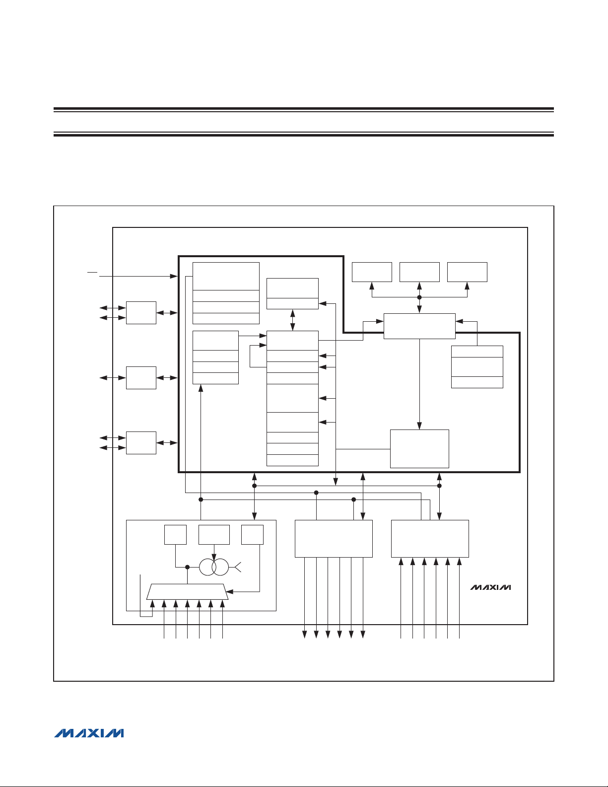
The MAX31782 system management microcontroller provides a complete solution for the monitoring and controlling
of complex system physical health characteristics. The MAX31782 is based on the high-performance 16-bit family of
MAXQM reduced instruction set computing (RISC) microcontrollers. The MAX31782 provides generous amounts of
flash program memory and SRAM data memory.
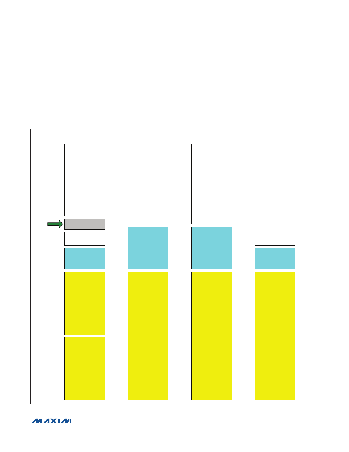
MAX31782 SYSTEM MANAGEMENT MICROCONTROLLER
RST
MSDA
MSCL
P6.n
n = 0−4
SCL
SDA
2
I
C
MASTER
GPIO
2
I
C
SLAVE
SYSTEM CLOCK
12-BIT
ADC
CLOCK CONTROL,
WATCHDOG TIMER, AND
POWER MONITOR
CKCN
WDCN
IC
INTERRUPT
LOGIC
IC IP
IMR
IIR
CURRENT
SOURCES
ADCH
STACK MEMORY
16 x 16
SP
ADDRESS
GENERATION
LOOP COUNTERS
LC[n]
BOOLEAN
VARIABLE
MANIPULATION
ACCUMULATORS
(16)
AP
APC
PSF
6-CHANNEL PULSE-WIDTH
MODULATOR
32KWords
FLASH
1KWords
SRAM
MEMORY MANAGEMENT
UNIT (MMU)
INSTRUCTION
DECODE
(src, dst TRANSPORT
DETERMINATION)
6-CHANNEL TACHOMETER
4KWords
UTILITY ROM
DATA POINTERS
DP[0], DP[1],
FP = (BP+OFFS)
DPC
MAXQ20 CORE
SYSTEM MODULES/
REGISTERS
V
INTERNAL TEMP
AD5P
MUX
AD4P
AD3P
AD2P
AD1P
DD
AD0P
MAXQ is a registered trademark of Maxim Integrated Products, Inc.
��������������������������������������������������������������� Maxim Integrated Products 1-1
PWM.5
PWM.4
PWM.3
PWM.2
PWM.1
PWM.0
TACH.5
TACH.4
TACH.3
TACH.2
TACH.1
MAX31782
TACH.0
Revision 0; 8/11
Page 4

MAX31782 User’s Guide
Some of the resources and features that the MAX31782 provides for monitoring and controlling a complex system
include the following:
• Remote temperature measurement of diode connected transistors on up to 6 channels
• Accurate voltage measurement using the 12-bit analog to digital converter (ADC) on up to 6 channels
• Internal temperature sensor
• Independent slave and master I2C-compatable interfaces
• Six independent PWM outputs and tachometer Inputs
• Hardware multiplier unit
• 32KWords of flash and 1KWords of SRAM memory
• Included ROM routines that allow bootloading and in-application programming flash memory
• In-system debugging
This document is provided as a supplement to the MAX31782 IC data sheet. This user’s guide provides the information
necessary to develop applications using the MAX31782. All electrical and timing specifications, pin descriptions, package information, and ordering information can be found in the MAX31782 IC data sheet.
��������������������������������������������������������������� Maxim Integrated Products 1-2
Revision 0; 8/11
Page 5

MAX31782 User’s Guide
SECTION 2: ARCHITECTURE
This section contains the following information:
2.1 Instruction Decoding . . . . . . . . . . . . . . . . . . . . . . . . . . . . . . . . . . . . . . . . . . . . . . . . . . . . . . . . . . . . . . . . . . . . . . .2-2
2.2 Register Space. . . . . . . . . . . . . . . . . . . . . . . . . . . . . . . . . . . . . . . . . . . . . . . . . . . . . . . . . . . . . . . . . . . . . . . . . . . .2-3
2.3 Memory Types . . . . . . . . . . . . . . . . . . . . . . . . . . . . . . . . . . . . . . . . . . . . . . . . . . . . . . . . . . . . . . . . . . . . . . . . . . . .2-4
2.3.1 Flash Memory . . . . . . . . . . . . . . . . . . . . . . . . . . . . . . . . . . . . . . . . . . . . . . . . . . . . . . . . . . . . . . . . . . . . . . . .2-4
2.3.2 SRAM Memory . . . . . . . . . . . . . . . . . . . . . . . . . . . . . . . . . . . . . . . . . . . . . . . . . . . . . . . . . . . . . . . . . . . . . . .2-5
2.3.3 Utility ROM . . . . . . . . . . . . . . . . . . . . . . . . . . . . . . . . . . . . . . . . . . . . . . . . . . . . . . . . . . . . . . . . . . . . . . . . . .2-5
2.3.4 Stack Memory. . . . . . . . . . . . . . . . . . . . . . . . . . . . . . . . . . . . . . . . . . . . . . . . . . . . . . . . . . . . . . . . . . . . . . . .2-5
2.4 Program and Data Memory Mapping and Access . . . . . . . . . . . . . . . . . . . . . . . . . . . . . . . . . . . . . . . . . . . . . . . .2-5
2.4.1 Program Memory Access. . . . . . . . . . . . . . . . . . . . . . . . . . . . . . . . . . . . . . . . . . . . . . . . . . . . . . . . . . . . . . .2-6
2.4.2 Program Memory Mapping . . . . . . . . . . . . . . . . . . . . . . . . . . . . . . . . . . . . . . . . . . . . . . . . . . . . . . . . . . . . .2-6
2.4.3 Data Memory Access. . . . . . . . . . . . . . . . . . . . . . . . . . . . . . . . . . . . . . . . . . . . . . . . . . . . . . . . . . . . . . . . . .2-6
2.4.3.1 Data Pointers . . . . . . . . . . . . . . . . . . . . . . . . . . . . . . . . . . . . . . . . . . . . . . . . . . . . . . . . . . . . . . . . . .2-6
2.4.3.2 Frame Pointer. . . . . . . . . . . . . . . . . . . . . . . . . . . . . . . . . . . . . . . . . . . . . . . . . . . . . . . . . . . . . . . . . .2-8
2.4.4 Data Memory Mapping . . . . . . . . . . . . . . . . . . . . . . . . . . . . . . . . . . . . . . . . . . . . . . . . . . . . . . . . . . . . . . . .2-8
2.4.4.1 Memory Map When Executing from Flash Memory . . . . . . . . . . . . . . . . . . . . . . . . . . . . . . . . . . . .2-9
2.4.4.2 Memory Map When Executing from Utility ROM . . . . . . . . . . . . . . . . . . . . . . . . . . . . . . . . . . . . . . .2-10
2.4.4.3 Memory Map When Executing from SRAM . . . . . . . . . . . . . . . . . . . . . . . . . . . . . . . . . . . . . . . . . . .2-11
2.5 Data Alignment. . . . . . . . . . . . . . . . . . . . . . . . . . . . . . . . . . . . . . . . . . . . . . . . . . . . . . . . . . . . . . . . . . . . . . . . . . . .2-12
2.6 Reset Conditions . . . . . . . . . . . . . . . . . . . . . . . . . . . . . . . . . . . . . . . . . . . . . . . . . . . . . . . . . . . . . . . . . . . . . . . . . .2-12
2.6.1 Power-On/Brownout Reset . . . . . . . . . . . . . . . . . . . . . . . . . . . . . . . . . . . . . . . . . . . . . . . . . . . . . . . . . . . . . .2-12
2.6.2 Watchdog Timer Reset. . . . . . . . . . . . . . . . . . . . . . . . . . . . . . . . . . . . . . . . . . . . . . . . . . . . . . . . . . . . . . . . .2-13
2.6.3 External Reset . . . . . . . . . . . . . . . . . . . . . . . . . . . . . . . . . . . . . . . . . . . . . . . . . . . . . . . . . . . . . . . . . . . . . . .2-13
2.6.4 Internal System Resets. . . . . . . . . . . . . . . . . . . . . . . . . . . . . . . . . . . . . . . . . . . . . . . . . . . . . . . . . . . . . . . . .2-13
2.7 Clock Generation . . . . . . . . . . . . . . . . . . . . . . . . . . . . . . . . . . . . . . . . . . . . . . . . . . . . . . . . . . . . . . . . . . . . . . . . . .2-14
2.8 Power Modes . . . . . . . . . . . . . . . . . . . . . . . . . . . . . . . . . . . . . . . . . . . . . . . . . . . . . . . . . . . . . . . . . . . . . . . . . . . . .2-14
LIST OF FIGURES
Figure 2-1. Instruction Word Format . . . . . . . . . . . . . . . . . . . . . . . . . . . . . . . . . . . . . . . . . . . . . . . . . . . . . . . . . . . . . .2-2
Figure 2-2. Program Memory Mapping . . . . . . . . . . . . . . . . . . . . . . . . . . . . . . . . . . . . . . . . . . . . . . . . . . . . . . . . . . . .2-7
Figure 2-3. Memory Map When Executing from Flash Memory . . . . . . . . . . . . . . . . . . . . . . . . . . . . . . . . . . . . . . . . .2-9
Figure 2-4. Memory Map When Executing from Utility ROM. . . . . . . . . . . . . . . . . . . . . . . . . . . . . . . . . . . . . . . . . . . .2-10
Figure 2-5. Memory Map When Executing from SRAM . . . . . . . . . . . . . . . . . . . . . . . . . . . . . . . . . . . . . . . . . . . . . . . .2-11
Figure 2-6. MAX31782 State Diagram . . . . . . . . . . . . . . . . . . . . . . . . . . . . . . . . . . . . . . . . . . . . . . . . . . . . . . . . . . . . .2-13
LIST OF TABLES
Table 2-1. Register-to-Register Transfer Operations. . . . . . . . . . . . . . . . . . . . . . . . . . . . . . . . . . . . . . . . . . . . . . . . . .2-4
Table 2-2. State of Circuits During Different Modes . . . . . . . . . . . . . . . . . . . . . . . . . . . . . . . . . . . . . . . . . . . . . . . . . .2-14
��������������������������������������������������������������� Maxim Integrated Products 2-1
Revision 0; 8/11
Page 6

MAX31782 User’s Guide
SECTION 2: ARCHITECTURE
The MAX31782 contains a MAXQ20 low-cost, high-performance, CMOS, fully static microcontroller with flash memory.
It is structured on a highly advanced, 16-accumulator-based, 16-bit RISC architecture. Fetch and execution operations
are completed in one cycle without pipelining, since the instruction contains both the op code and data. The highly
efficient core is supported by 16 accumulators and a 16-level hardware stack, enabling fast subroutine calling and task
switching.
Data can be quickly and efficiently manipulated with three internal data pointers. Two of these data pointers, DP0 and
DP1, are stand-alone 16-bit pointers. The third data pointer, frame pointer, is composed of a 16-bit base pointer (BP)
and an 8-bit offset register (OFFS). All three pointers support postincrement/decrement functionality for read operations
and preincrement/decrement for write operations. For the frame pointer (FP = BP[OFFS]), the increment/decrement
operation is executed on the OFFS register and does not affect the base pointer. Multiple data pointers allow more than
one function to access data memory without having to save and restore data pointers each time.
Stack functionality is provided by dedicated memory with a 16-bit width and a depth of 16. An on-chip memory management unit (MMU) allows logical remapping of the program and data spaces, and thus facilitates in-system programming
and fast access to data tables, arrays, and constants located in flash memory.
This section provides details on the following topics.
1) Instruction decoding
2) Register space
3) Memory types
4) Program and data memory mapping and access
5) Data alignment
6) Reset conditions
7) Clock generation
8) Power modes
2.1 Instruction Decoding
The MAX31782 uses the standard 16-bit MAXQ20 core instruction set, which is described in SECTION 20: Instruction
Set Summary. Every instruction is encoded as a single 16-bit word. The instruction word format is shown in Figure 2-1.
FORMAT DESTINATION SOURCE
f d d d d d d d s s s s s s s s
Figure 2-1. Instruction Word Format
Bit 15 (f) indicates the format for the source field of the instruction as follows:
If f equals 0, the instruction is an immediate source instruction. The source field represents an immediate 8-bit value.
If f equals 1, the instruction is a register source instruction. The source field represents the register from which the
source value is read.
Bits 14 to 8 (ddddddd) represent the destination for the transfer. This value always represents a destination register. The
lower four bits contain the module specifier and the upper three bits contain the register index in that module.
Bits 7 to 0 (ssssssss) represent the source for the transfer. Depending on the value of the format field, this can either
be an immediate value or a source register. If this field represents a register, the lower four bits contain the module
specifier and the upper four bits contain the register index in that module.
��������������������������������������������������������������� Maxim Integrated Products 2-2
Revision 0; 8/11
Page 7

MAX31782 User’s Guide
This instruction word format presents the following limitations.
1) There are 32 registers per register module, but only 4 bits are allocated to designate the source register and only 3
bits are allocated to designate the destination register.
2) The source field only provides 8 bits of data for an immediate value; however, a 16-bit immediate value can be
required.
The MAX31782 uses a prefix register (PFX) to address these limitations. The PFX register provides the additional bits
required to access all 32 registers within a module. The PFX register also provides the additional 8 bits of data required
to make a 16-bit immediate data source. The data that is written to the PFX register survives for only one clock cycle.
This means the write to the PFX register must occur immediately prior to the instruction requiring the PFX register. The
PFX register is cleared to zero after one cycle so it does not affect any other instructions. The write to the PFX register is
done automatically by the assembler and requires one additional execution cycle. So, while most instructions execute
in a single cycle, two cycles are needed for instructions that require the PFX register.
The architecture of the MAX31782 is transport-triggered. This means that writing to or reading from certain register
locations also causes side effects to occur. These side effects form the basis of the MAX31782’s higher level op codes,
such as ADDC, OR, and JUMP. While these op codes are actually implemented as MOVE instructions between certain register locations, the encoding is handled by the assembler and need not be a concern to the programmer. The
unused “empty” locations in the system register modules are used for these higher level op codes.
The instruction set is designed to be highly orthogonal. All arithmetic and logical operations that use two registers can
use any register along with the accumulator. Data can be transferred between any two registers in a single instruction.
2.2 Register Space
The MAX31782 provides a total of 13 register modules broken up into two different groups. These groupings are
descriptive only, as there is no difference between accessing the two register groups from a programming perspective.
The two groups are:
1) Peripheral Registers: These are the lower six modules (Modules 0h through 5h). The peripheral registers in the
MAX31782 are used for functionalities such as ADC, PWM outputs, tachometer inputs, GPIO, etc. The peripheral
registers are not used to implement op codes.
2) System Registers: These are modules 8h, 9h, and Bh through Fh. The system registers in the MAX31782 are used
to implement higher level op codes as well as the following common system features.
• 16-bit ALU and associated status flags (zero, equals, carry, sign, overflow)
• 16 working accumulator registers, each 16-bit, along with associated control registers
• Instruction pointer
• Registers for interrupt control, handling, and identification
• Auto-decrementing loop counters for fast, compact looping
• Two data pointer registers and a frame pointer for data memory access
Each system register module has 16 registers, while each peripheral register module has 32 registers. The number of
cycles required to access a particular register depends upon the register’s index within the module. The access times
based upon the register index are grouped as follows:
• The first eight registers (index 0h to 7h) in each module can be read from or written to in a single cycle.
• The second eight registers (index 8h to 0Fh) can be read from in a single cycle and written to in two cycles (by using
the PFX register).
• The last 16 registers (10h to 1Fh) in peripheral register modules can be read or written in two cycles (always requiring use of the PFX register).
��������������������������������������������������������������� Maxim Integrated Products 2-3
Revision 0; 8/11
Page 8

MAX31782 User’s Guide
Registers can be 8 or 16 bits in length. Some registers can contain reserved bits. The user should not write to any
reserved bits. Data transfers between registers of different sizes are handled as shown in Table 2-1.
• If the source and destination registers are both 8 bits wide, data is copied bit to bit.
• If the source register is 8 bits wide and the destination register is 16 bits wide, the data from the source register is
transferred into the lower 8 bits of the destination register. The upper 8 bits of the destination register are set to the
current value of the PFX register; this value is normally zero, but it can be set to a different value by the previous
instruction if needed. The PFX register reverts back to zero after one cycle, so this must be done by the instruction
immediately before the one that is using the value.
• If the source register is 16 bits wide and the destination register is 8 bits wide, the lower 8 bits of the source are
transferred to the destination register.
• If both registers are 16 bits wide, data is copied bit to bit.
The above rules apply to all data movements between defined registers. Data transfer to/from undefined register locations has the following behavior:
• If the destination is an undefined register, the MOVE is a dummy operation but can trigger an underlying operation
according to the source register (e.g., @DPn--).
• If the destination is a defined register and the source is undefined, the source data for the transfer depends upon
the source module width. If the source is from a module containing 8-bit or 8-bit and 16-bit source registers, the
source data is equal to the prefix data as the upper 8 bits and 00h as the lower 8 bits. If the source is from a module
containing only 16-bit source registers, 0000h source data is used for the transfer.
Table 2-1. Register-to-Register Transfer Operations
SOURCE REGISTER SIZE
(BITS)
8 8 X — Source [7:0]
8 16 No 00h Source [7:0]
8 16 Yes PFX [7:0] Source [7:0]
16 8 X — Source [7:0]
16 16 X Source [15:8] Source [7:0]
DESTINATION REGISTER SIZE
(BITS)
PREFIX
SET?
DESTINATION SET TO VALUE
HIGH 8 BITS LOW 8 BITS
2.3 Memory Types
In addition to the internal register space, the MAX31782 incorporates the following memory types:
• 32KWords of flash memory
• 1KWords of SRAM
• 4KWords of utility ROM contain a debugger and program loader
• 16-level stack memory for storage of program return addresses and general-purpose use
The memory on the MAX31782 is organized according to a Harvard architecture. This means that there are separate busses for both program and data memory. Stack memory is also separate and is accessed through a dedicated register set.
2.3.1 Flash Memory
The MAX31782 contains 32KWords (32K x 16) of flash memory. The flash memory begins at address 0000h and is
contiguous through word address 7FFFh. The flash memory can also be used for storing lookup tables and other nonvolatile data.
The incorporation of flash memory allows the contents of the flash memory to be upgraded in the field, either by the
application or by one of the bootloaders (JTAG or I2C). Writing to flash memory must be done indirectly by using routines that are provided by the utility ROM. See SECTION 21: Utility ROM and SECTION 18: In-System Programming for
more details.
��������������������������������������������������������������� Maxim Integrated Products 2-4
Revision 0; 8/11
Page 9

MAX31782 User’s Guide
2.3.2 SRAM Memory
The MAX31782 contains 1KWords (1K x 16) of SRAM memory. The SRAM memory address begins at address 0000h
and is contiguous through word address 03FFh. The contents of the SRAM are indeterminate after power-on reset, but
are maintained during stop mode and non-POR resets.
When using the in-circuit debugging features, the highest 19 bytes of the SRAM must be reserved for saved state
storage and working space for the debugging routines. If in-circuit debug is not used, the entire 1KWords of SRAM is
available for application use.
2.3.3 Utility ROM
The utility ROM is a 4KWord segment of memory. The utility ROM memory address begins at word address 8000h and
is contiguous through word address 8FFFh. The utility ROM is programmed at the factory and cannot be modified. The
utility ROM provides the following system utility functions:
• Reset vector (not user code reset vector)
• In-system programming (bootstrap loader) over JTAG or I2C-compatible interfaces
• In-circuit debug routines
• Routines for in-application flash programming
Following any reset, the MAX31782 automatically starts execution at the reset vector, which is address 8000h in the utility
ROM. The ROM code determines whether the program execution should immediately jump to the start of application code
(flash address 0000h), or to one of the special routines mentioned. Routines within the utility ROM are firmware-accessible
and can be called as subroutines by the application software. See SECTION 21: Utility ROM, SECTION 18: In-System
Programming, and SECTION 17: In-Circuit Debug Mode for more information on the routines provided by the utility ROM.
2.3.4 Stack Memory
A 16-bit, 16-level on-chip stack provides storage for program return addresses and general-purpose use. The stack is
used automatically by the processor when the CALL, RET, and RETI instructions are executed, and when an interrupt is
serviced. The stack can also be used explicitly to store and retrieve data by using the @SP- - source, @++SP destination, or the PUSH, POP, and POPI instructions. The POPI instruction acts identically to the POP instruction except that
it additionally clears the INS bit.
The width of the stack is 16 bits to accommodate the instruction pointer size. On reset, the stack pointer SP initializes
to the top of the stack (0Fh). The CALL, PUSH, and interrupt vectoring operations first increment SP and then store a
value at @SP. The RET, RETI, POP, and POPI operations first retrieve the value at @SP and then decrement SP.
The stack memory is initialized to indeterminate values upon reset or power-up. Stack memory is dedicated for stack
operations only and cannot be accessed by the MAX31782 program or data busses.
When using the in-circuit debugging features, one word of the stack must be reserved for the debugging routines. If
in-circuit debug is not used, the entire stack is available for application use.
2.4 Program and Data Memory Mapping and Access
The memory on the MAX31782 is implemented using a Harvard architecture, with separate buses for program and data
memory. The memory management unit (MMU) allows the MAX31782 to also support a pseudo-Von Neumann memory
map. The pseudo-Von Neumann memory map allows each of the memory segments (flash, SRAM, and utility ROM) to
be logically mapped into a single contiguous memory map. This allows all the memory segments to be accessed as
both program and memory data. The advantages the pseudo-Von Neumann memory map provides are:
• Program execution can occur from the flash, SRAM, or utility ROM memory segments.
• The SRAM and flash memory segments can both be used for data memory.
Using the pseudo-Von Neumann memory map does have one restriction. This restriction is that a particular memory
segment cannot be simultaneously accessed as both program and data memory.
��������������������������������������������������������������� Maxim Integrated Products 2-5
Revision 0; 8/11
Page 10

MAX31782 User’s Guide
2.4.1 Program Memory Access
The instructions that the MAX31782 is executing reside in what is defined as the program memory. The MMU fetches
the instructions using the program bus. The instruction pointer (IP) register designates the program memory address of
the next instruction to fetch. The IP register is read/write accessible by the user software. A write to the IP register forces
program flow to the new address on the next cycle following the write. The content of the IP register is incremented
by 1 automatically after each fetch operation. From an implementation perspective, system interrupts and branching
instructions simply change the contents of the IP register and force the op code to fetch from a new program location.
2.4.2 Program Memory Mapping
The MAX31782’s mapping of the three memory segments (flash, SRAM, and utility ROM) as program memory is shown
in Figure 2-2. The mapping of memory segments into program space is always the same. When referring to memory
as program memory, all addresses are given as word addresses. The 32KWord flash memory segment is located at
memory location 0000h through 7FFFh and is logically divided into two pages, each containing 16KWords. The utility
ROM is located from location 8000h through 8FFFh, followed by the SRAM memory segment at location A000h through
A3FFh. The user code reset vector, which is the first instruction of user program code that is executed, is located at
flash memory address 0000h. User program code should always begin at this address.
2.4.3 Data Memory Access
Data memory mapping and access control are handled by the memory management unit (MMU). Read/write access
to data memory can be in word or in byte mode. The MAX31782 provides three pointers that can be used for indirect
accessing of data memory. The MAX31782 has two data pointers (@DPn) and one frame pointer (@BP[OFFS]). These
pointers are implemented as registers that can be directly accessed by user software. A data memory access requires
only one system clock period.
2.4.3.1 Data Pointers
To access data memory, the data pointers are used as one of the operands in a MOVE instruction. If the data pointer is
used as a source, the core performs a load operation that reads data from the memory location addressed by the data
pointer. If the data pointer is used as destination, the core performs a store operation that writes data to the memory
location addressed by the data pointer. Following are some examples of setting and using a data pointer.
moveDP[0], #0100h ;set pointerDP[0]toaddress100h
moveAcc, @DP[0] ;readdatafromlocation100h
move@DP[0], Acc ;writetolocation100h
The address pointed to by the data pointers can be automatically incremented or decremented. If the data pointer is
used as a source, the pointer can be incremented or decremented after the data access. If the data pointer is used as
a destination, the increment or decrement can occur prior to the data access. Following are examples of using the data
pointers increment/decrement features.
moveAcc, @DP[0]++ ;increment DP[0]afterread
moveAcc, @DP[1]-- ;decrement DP[1]afterread
move@++DP[0], Acc ;increment DP[0]beforewrite
move@--DP[1], Acc ;decrement DP[0]beforewrite
��������������������������������������������������������������� Maxim Integrated Products 2-6
Revision 0; 8/11
Page 11
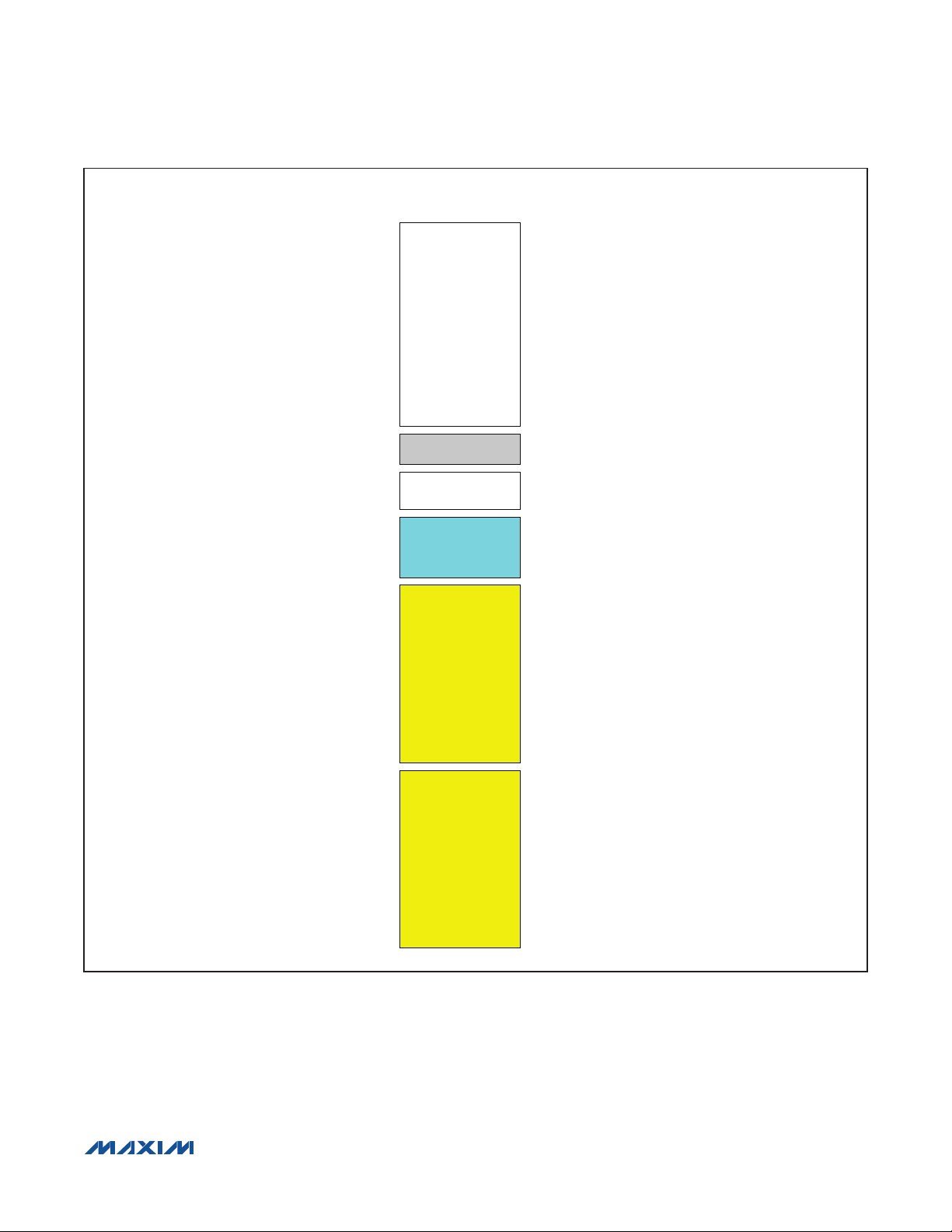
PROGRAM
SPACE
MAX31782 User’s Guide
FFFFh
1K x 16
SRAM
4K x 16
UTILITY ROM
16K x 16
FLASH
(PAGE 1)
16K x 16
FLASH
(PAGE 0)
A3FFh
A000h
8FFFh
8000h
7FFFh
4000h
3FFFh
Figure 2-2. Program Memory Mapping
��������������������������������������������������������������� Maxim Integrated Products 2-7
0000h
Revision 0; 8/11
Page 12

MAX31782 User’s Guide
2.4.3.2 Frame Pointer
The frame pointer (BP[OFFS]) is formed by the 16-bit unsigned addition of the 16-bit frame pointer base register (BP)
and the 8-bit frame pointer offset register (OFFS). The method the MAX31782 uses to access data using the frame
pointer is similar to the data pointers. When increments or decrements are used, only the value of OFFS is incremented
or decremented. The base pointer (BP) remains unaffected by increments or decrements of the OFFS register, including when the OFFS register rolls over from FFh to 00h or from 00h to FFh. Following are examples of how to use the
frame pointer.
moveBP, #0100h ;setbasepointer toaddress100h
moveOFFS, #10h ;settheoffset to10h,
moveAcc, @BP[OFFS] ;read datafromlocation0110h
move@BP[OFFS], Acc ;write datatolocation0110h
moveAcc, @BP[OFFS++] ;increment OFFSafterread
moveAcc, @BP[OFFS++] ;decrement OFFSafterread
move@BP[++OFFS], Acc ;increment OFFSbeforewrite
move@BP[--OFFS], Acc ;decrement OFFSbeforewrite
2.4.4 Data Memory Mapping
The MAX31782’s pseudo-Von Neumann memory map allows the MMU to read data from each of the three memory segments (flash, SRAM, utility ROM). The MMU can also write data directly to the SRAM memory segment. Data memory
can be written to the flash memory segment, but because writing to flash requires the use of the utility ROM routines,
this is not a direct access. The logical mapping of the three memory segments as data memory varies depending upon:
• from which memory segment instructions are currently being executed
• if data memory is being accessed in word or byte mode
In all cases, whichever memory segment is currently being used as program memory cannot be accessed as data
memory.
When the program is currently executing instructions from either the SRAM or utility ROM memory segments, the flash
memory is mapped to half the data memory space. If word access mode is selected, both pages (32KWords) can
be logically mapped to data memory space. If byte access mode is selected, only one page (32KB) can be logically
mapped to half of the data memory space. When operating in byte access mode, the selection of which flash page is
mapped into data memory space is determined by the code data access bit (CDA0):
CDA0 SELECTED PAGE IN BYTE MODE SELECTED PAGE IN WORD MODE
0 P0 P0 and P1
1 P1 P0 and P1
The next three sections detail the mapping of the different memory segments as data memory depending upon from
which memory segment instructions are currently being executed.
��������������������������������������������������������������� Maxim Integrated Products 2-8
Revision 0; 8/11
Page 13
MAX31782 User’s Guide
2.4.4.1 Memory Map When Executing from Flash Memory
When executing from the flash memory:
• Read and write operations of SRAM memory are executed normally.
• The utility ROM can be read as data, starting at 8000h of the data space. The utility ROM cannot be written.
Figure 2-3 illustrates the mapping of the SRAM and utility ROM memory segments into data memory space when code
is executing from the flash memory segment.
PROGRAM
SPACE
1K x 16
SRAM
4K x 16
UTILITY ROM
DATA SPACE
(BYTE MODE)
FFFFh FFFFh FFFFh
A3FFh
A000h
8FFFh
8000h 8000h
7FFFh 7FFFh
8K x 8
UTILITY ROM
9FFFh
DATA SPACE
(WORD MODE)
8FFFh
4K x 16
UTILITY ROM
8000h
7FFFh
16K x 16
FLASH
(PAGE 1)
4000h
3FFFh
EXECUTING FROM
16K x 16
FLASH
(PAGE 0)
0000h 0000h 0000h
Figure 2-3. Memory Map When Executing from Flash Memory
��������������������������������������������������������������� Maxim Integrated Products 2-9
2K x 8
SRAM
07FFh
1K x 16
SRAM
03FFh
Revision 0; 8/11
Page 14
MAX31782 User’s Guide
2.4.4.2 Memory Map When Executing from Utility ROM
When executing from the utility ROM:
• Read and write operations of SRAM memory are executed normally.
• Reading of flash memory is executed normally. Writing to flash memory requires the use of the utility ROM routines.
• One page (byte access mode) or both pages (word access mode) of the flash memory can be accessed as data
with an offset of 8000h as determined by the CDA0 bit.
Figure 2-4 illustrates the mapping of the SRAM and flash memory segments into data memory space when code is
executing from the utility ROM memory segment.
EXECUTING FROM
PROGRAM
SPACE
1K x 16
SRAM
4K x 16
UTILITY ROM
16K x 16
FLASH
(PAGE 1)
DATA SPACE
(BYTE MODE, CDA0 = 0)
FFFFh FFFFh FFFFh
32K x 8
LOWER HALF
(PAGE 0) OF
FLASH
A3FFh
A000h
8FFFh
8000h 8000h 8000h
7FFFh
DATA SPACE
(BYTE MODE, CDA0 = 1)
32K x 8
UPPER HALF
(PAGE 1) OF
FLASH
DATA SPACE
(WORD MODE)
FFFFh
32K x 16
FLASH
8000h
4000h
3FFFh
16K x 16
FLASH
(PAGE 0)
2K x 8
SRAM
0000h 0000h
Figure 2-4. Memory Map When Executing from Utility ROM
�������������������������������������������������������������� Maxim Integrated Products 2-10
07FFh
2K x 8
SRAM
07FFh
1K x 16
0000h 0000h
SRAM
03FFh
Revision 0; 8/11
Page 15
MAX31782 User’s Guide
2.4.4.3 Memory Map When Executing from SRAM
When executing from the SRAM:
The utility ROM can be read as data, starting at 8000h of the data space. The utility ROM cannot be written.
Reading of flash memory is executed normally. Writing to flash memory requires the use of the utility ROM routines.
One page (byte access mode) or both pages (word access mode) of the flash memory can be accessed as data with
an offset of 0000h. For byte access mode, the page of flash accessed is determined by the CDA0 bit.
Figure 2-5 illustrates the mapping of the flash and utility ROM memory segments into data memory space when code
is executing from the SRAM memory segment.
EXECUTING FROM
PROGRAM
SPACE
1K x 16
SRAM
4K x 16
UTILITY ROM
16K x 16
FLASH
(PAGE 1)
DATA SPACE
(BYTE MODE, CDA0 = 0)
FFFFh FFFFh FFFFh FFFFh
A3FFh
A000h
8FFFh
8000h
7FFFh
8K x 8
UTILITY ROM
8000h
7FFFh
DATA SPACE
(BYTE MODE, CDA0 = 1)
8K x 8
UTILITY ROM
9FFFh9FFFh
8000h
7FFFh
DATA SPACE
(WORD MODE)
8FFFh
4K x 16
UTILITY ROM
8000h
7FFFh
4000h
3FFFh
16K x 16
FLASH
(PAGE 0)
0000h 0000h 0000h 0000h
LOWER HALF
(PAGE 0) OF
Figure 2-5. Memory Map When Executing from SRAM
�������������������������������������������������������������� Maxim Integrated Products 2-11
32K x 8
FLASH
32K x 8
UPPER HALF
(PAGE 1) OF
FLASH
32K x 16
FLASH
Revision 0; 8/11
Page 16

MAX31782 User’s Guide
2.5 Data Alignment
To support merged program and data memory operation while maintaining efficient memory space usage, the data
memory must be able to support both byte and word mode accessing. Data is aligned in data memory as words, but
the effective data address is resolved to bytes. This data alignment allows program instruction fetching in words while
maintaining data accessibility at the byte level. It is important to realize that this accessibility requires strict word alignment. All executable or data words must align to an even address in byte mode. Care must be taken when updating a
code segment as misalignment of words likely results in loss of program execution control.
Memory is always read as a complete word, whether for program fetch or data access. The program decoder always
uses a full 16-bit word. The data access can utilize a word or an individual byte. Data memory is organized as two bytewide memory banks with common word address decode but two 8-bit data buses. In byte mode, data pointer hardware
reads out the full word containing the selected byte using the effective data word address pointer (the least significant
bit of the byte data pointer is not initially used). Then, the least significant data pointer bit functions as the byte select
that is used to place the correct byte on the data bus. For write access, data pointer hardware addresses a particular
word using the effective data word address while the least significant bit selects the corresponding data bank for write.
The contents of the other byte are left unaffected.
2.6 Reset Conditions
The MAX31782 has several possible sources of reset:
• Power-On/Brownout Reset
• Watchdog Timer Reset
• External Reset
• Internal System Reset
Once a reset condition has completed or been removed, code execution begins at the beginning of utility ROM, which
is address 8000h. The utility ROM code interrogates the I2C_SPE, JTAG_SPE, and PWL bits to determine if bootloading
is necessary. If bootloading is not required, execution jumps to the user code reset vector, which is at flash memory
address 0000h.
The RST pin is an output as well as an input. If a reset condition is generated by one of the MAX31782’s internal reset
sources (brownout, watchdog timer, or internal reset), an output reset pulse is generated on the RST pin while the
MAX31782 remains in reset.
2.6.1 Power-On/Brownout Reset
The MAX31782 provides a power-on reset (POR) circuit to ensure proper initialization of internal device states and analog circuits. The POR voltage threshold range is between approximately 1.1V and 1.7V. When VDD is below the POR
level, the state of all the MAX31782 pins, including RST, is indeterminate.
The MAX31782 also includes brownout detection capability. This is an on-chip precision reference and comparator that
monitors the supply voltage, VDD, to ensure that it is within acceptable limits. If VDD is below the brownout level (VBO),
the power monitor generates a reset. This can occur when:
• The MAX31782 is being powered up and VDD is above the POR level but still less than VBO.
• VDD drops from an acceptable level to less than VBO.
Once VDD exceeds VBO, the MAX31782 exits the reset condition and the internal oscillator starts up. After approximately 1000 clock cycles (t
• All registers and circuits enter their reset state.
• The POR flag in the watchdog control register (WDCN) is set to indicate the source of the reset.
• The MAX31782 begins normal operation (CPU state).
• Code execution begins at utility ROM location 8000h.
The transition between POR, brownout, and normal operation is detailed in Figure 2-6. Note: If VDD is below VBO, there
is a chance that the SRAM was corrupted. If the POR flag in WDCN is set, all data in SRAM should be reinitialized.
�������������������������������������������������������������� Maxim Integrated Products 2-12
SU:MOSC
) the MAX31782 performs the following tasks.
Revision 0; 8/11
Page 17
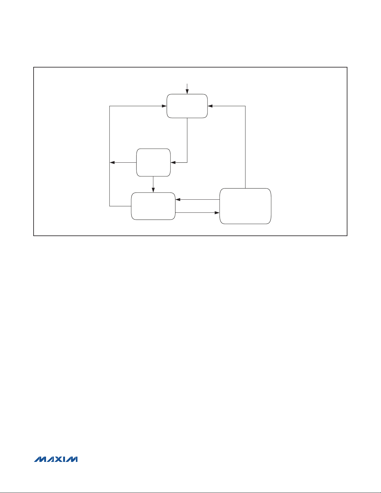
VDD < V
VDD < V
BO
STARTUP DELAY
DIGITAL CORE ON
BO
CODE IS EXECUTING
SYSTEM CLOCK
t
SU:MOSC
CPU MODE
ANALOG ON
POR
BROWNOUT STATE
CPU DISABLED
ANALOG ACTIVE
> V
V
DD
BO
PORT6 GPIO INT, I2C
START INT, SVM INT
OR EXT RESET
CKCN.STOP = 1
MAX31782 User’s Guide
VDD < V
BO
STOP MODE
DIGITAL CORE OFF
ANALOG ON
SVM MONITOR DEPENDS
ON SVMEN AND SVMSTOP
Figure 2-6. MAX31782 State Diagram
2.6.2 Watchdog Timer Reset
The watchdog timer is a programmable hardware timer that can be used to reset the processor in case a software
lockup or other unrecoverable error occurs. Once the watchdog is enabled, software must reset the watchdog timer
periodically. If the processor does not reset the watchdog timer before it elapses, the watchdog can initiate a reset.
If the watchdog resets the processor, the MAX31782 remains in reset and holds the RST pin low for 12 clock cycles.
When a reset occurs due to a watchdog timeout, the watchdog timer reset flag (WTRF) in the WDCN register is set to
indicate the source of the reset.
2.6.3 External Reset
During normal operation, the MAX31782 is placed into external reset when the RST pin is held at logic 0 for at least four
clock cycles. Once the MAX31782 enters reset mode, it remains in reset as long as the RST pin is held at logic 0. After
the RST pin returns to logic 1, the processor exits reset within 12 clock cycles.
An external reset pulse on the RST pin can also bring the MAX31782 out of its low-power stop mode. When this occurs,
the MAX31782 resets and returns to normal CPU mode operation within 10 clock cycles.
2.6.4 Internal System Resets
There are two possible sources of internal system resets. An internal reset holds the MAX31782 in reset mode for 12
clock cycles.
1) When data BBh is written to the special I2C slave address 34h.
2) When in-system programming is complete and the ROD bit is set to 1.
�������������������������������������������������������������� Maxim Integrated Products 2-13
Revision 0; 8/11
Page 18

MAX31782 User’s Guide
2.7 Clock Generation
The MAX31782 generates its 4MHz instruction clock using an internal oscillator. This oscillator starts up when VDD
exceeds the brownout voltage level, VBO. There is a delay of approximately 1000 clock cycles (t
SU:MOSC
when the oscillator starts and when clocking of the MAX31782 begins. This delay ensures that the clock is stable prior
to beginning normal operation.
2.8 Power Modes
The MAX31782 has two modes of operation. These two modes of operation are detailed in the state diagram as shown
in Figure 2-6.
1) Normal CPU mode
2) Stop mode
The MAX31782 enters stop mode when the STOP bit in the system clock control register (CKCN) is set. Upon entering
stop mode, the digital core is no longer clocked, thus making the core inactive. In stop mode, the ADC is also disabled
and the Supply Voltage Monitor (SVM) can be disabled. The internal oscillator, brownout detection, and regulators
(REG18 and REG25 pins) remain active during stop mode. Table 2-2 details the state of the MAX31782’s analog and
digital blocks during the different modes of operation.
Table 2-2. State of Circuits During Different Modes
CKCN.STOP SVM.SVMEN SVM.SVMSTOP
0 0 X
0 1 X
1 0 X
1 1 0
1 1 1
POWER
MODE
CPU
Mode
CPU
Mode
Stop
Mode
Stop
Mode
Stop
Mode
REGULATORS
CPU
1.8V 2.5V
On On On On On Off On/Off
On On On On On On On/Off
Off On On On On Off Off
Off On On On On Off Off
Off On On On On On Off
INTERNAL
OSCILLATOR
BROWNOUT
DETECTION
MONITOR
SVM
) between
ADC
The MAX31782 exits stop mode when any of the following interrupt conditions occurs:
• GPIO interrupt from Port 6
• I2C START interrupt
• SVM interrupt
• External reset
The interrupt sources listed must be enabled prior to entering stop mode if they are going to be used to bring the
MAX31782 out of stop mode. After receiving one of these interrupts, the MAX31782 exits stop mode and returns to CPU
mode within 10 system clock cycles. If an interrupt causes the system to come out of stop mode, the program execution
starts from the point where stop mode was asserted. However, if an external reset is used to come out of stop mode,
the program execution begins from utility ROM location 8000h.
�������������������������������������������������������������� Maxim Integrated Products 2-14
Revision 0; 8/11
Page 19

MAX31782 User’s Guide
SECTION 3: SYSTEM REGISTER DESCRIPTIONS
This section contains the following information:
3.1 System Register Bit Descriptions. . . . . . . . . . . . . . . . . . . . . . . . . . . . . . . . . . . . . . . . . . . . . . . . . . . . . . . . . . . . . .3-4
3.1.1 Accumulator Pointer Register (AP, 8h[0h]) . . . . . . . . . . . . . . . . . . . . . . . . . . . . . . . . . . . . . . . . . . . . . . . . .3-4
3.1.2 Accumulator Pointer Control Register (APC, 8h[1h]). . . . . . . . . . . . . . . . . . . . . . . . . . . . . . . . . . . . . . . . . .3-4
3.1.3 Processor Status Flags Register (PSF, 8h[4h]) . . . . . . . . . . . . . . . . . . . . . . . . . . . . . . . . . . . . . . . . . . . . . .3-5
3.1.4 Interrupt and Control Register (IC, 8h[5h]) . . . . . . . . . . . . . . . . . . . . . . . . . . . . . . . . . . . . . . . . . . . . . . . . .3-5
3.1.5 Interrupt Mask Register (IMR, 8h[6h]) . . . . . . . . . . . . . . . . . . . . . . . . . . . . . . . . . . . . . . . . . . . . . . . . . . . . .3-6
3.1.6 System Control Register (SC, 8h[8h]) . . . . . . . . . . . . . . . . . . . . . . . . . . . . . . . . . . . . . . . . . . . . . . . . . . . . .3-6
3.1.7 Interrupt Identification Register (IIR, 8h[Bh]) . . . . . . . . . . . . . . . . . . . . . . . . . . . . . . . . . . . . . . . . . . . . . . . .3-7
3.1.8 System Clock Control Register (CKCN, 8h[Eh]) . . . . . . . . . . . . . . . . . . . . . . . . . . . . . . . . . . . . . . . . . . . . .3-7
3.1.9 Watchdog Control Register (WDCN, 8h[Fh]) . . . . . . . . . . . . . . . . . . . . . . . . . . . . . . . . . . . . . . . . . . . . . . . .3-8
3.1.10 Accumulator n Register (A[n], 9h[nh]) . . . . . . . . . . . . . . . . . . . . . . . . . . . . . . . . . . . . . . . . . . . . . . . . . . . .3-9
3.1.11 Prefix Register (PFX[n], Bh[n]) . . . . . . . . . . . . . . . . . . . . . . . . . . . . . . . . . . . . . . . . . . . . . . . . . . . . . . . . . .3-9
3.1.12 Instruction Pointer Register (IP, Ch[0h]) . . . . . . . . . . . . . . . . . . . . . . . . . . . . . . . . . . . . . . . . . . . . . . . . . .3-9
3.1.13 Stack Pointer Register (SP, Dh[1h]) . . . . . . . . . . . . . . . . . . . . . . . . . . . . . . . . . . . . . . . . . . . . . . . . . . . . . .3-10
3.1.14 Interrupt Vector Register (IV, Dh[2h]) . . . . . . . . . . . . . . . . . . . . . . . . . . . . . . . . . . . . . . . . . . . . . . . . . . . .3-10
3.1.15 Loop Counter 0 Register (LC[0], Dh[6h]) . . . . . . . . . . . . . . . . . . . . . . . . . . . . . . . . . . . . . . . . . . . . . . . . .3-10
3.1.16 Loop Counter 1 Register (LC[1], Dh[7h]) . . . . . . . . . . . . . . . . . . . . . . . . . . . . . . . . . . . . . . . . . . . . . . . . .3-10
3.1.17 Frame Pointer Offset Register (OFFS, Eh[3h]). . . . . . . . . . . . . . . . . . . . . . . . . . . . . . . . . . . . . . . . . . . . . .3-10
3.1.18 Data Pointer Control Register (DPC, Eh[4h]) . . . . . . . . . . . . . . . . . . . . . . . . . . . . . . . . . . . . . . . . . . . . . . .3-11
3.1.19 General Register (GR, Eh[5h]) . . . . . . . . . . . . . . . . . . . . . . . . . . . . . . . . . . . . . . . . . . . . . . . . . . . . . . . . . .3-11
3.1.20 General Register Low Byte (GRL, Eh[6h]) . . . . . . . . . . . . . . . . . . . . . . . . . . . . . . . . . . . . . . . . . . . . . . . . .3-11
3.1.21 Frame Pointer Base Register (BP, Eh[7h]). . . . . . . . . . . . . . . . . . . . . . . . . . . . . . . . . . . . . . . . . . . . . . . . .3-12
3.1.22 General Register Byte-Swapped (GRS, Eh[8h]) . . . . . . . . . . . . . . . . . . . . . . . . . . . . . . . . . . . . . . . . . . . .3-12
3.1.23 General Register High Byte (GRH, Eh[9h]) . . . . . . . . . . . . . . . . . . . . . . . . . . . . . . . . . . . . . . . . . . . . . . . .3-12
3.1.24 General Register Sign Extended Low Byte (GRXL, Eh[Ah]) . . . . . . . . . . . . . . . . . . . . . . . . . . . . . . . . . . .3-12
3.1.25 Frame Pointer Register (FP, Eh[Bh]) . . . . . . . . . . . . . . . . . . . . . . . . . . . . . . . . . . . . . . . . . . . . . . . . . . . . .3-12
3.1.26 Data Pointer 0 Register (DP[0], Fh[3h]) . . . . . . . . . . . . . . . . . . . . . . . . . . . . . . . . . . . . . . . . . . . . . . . . . . .3-12
3.1.27 Data Pointer 1 Register (DP[1], Fh[7h]) . . . . . . . . . . . . . . . . . . . . . . . . . . . . . . . . . . . . . . . . . . . . . . . . . . .3-13
LIST OF TABLES
Table 3-1. System Register Map . . . . . . . . . . . . . . . . . . . . . . . . . . . . . . . . . . . . . . . . . . . . . . . . . . . . . . . . . . . . . . . . .3-2
Table 3-2. System Register Bit Functions . . . . . . . . . . . . . . . . . . . . . . . . . . . . . . . . . . . . . . . . . . . . . . . . . . . . . . . . . .3-3
��������������������������������������������������������������� Maxim Integrated Products 3-1
Revision 0; 8/11
Page 20

MAX31782 User’s Guide
SECTION 3: SYSTEM REGISTER DESCRIPTIONS
Most MAX31782 functions are controlled by sets of registers. These registers provide a working space for memory operations as well as configuring and addressing peripheral registers on the device. Registers are divided into two major
types: system registers and peripheral registers. The common register set, also known as the system registers, includes
ALU access and control registers, accumulator registers, data pointers, interrupt vectors and control, and stack pointer.
The peripheral registers define additional functionality and the functionality is broken up into discrete modules.
This section describes the MAX31782’s system registers. Table 3-1 shows the MAX31782 system register map.
Table 3-2 explains system register bit functions. This is followed by a detailed bit description.
Table 3-1. System Register Map
REGISTER
INDEX
00h AP A[0] PFX[0] IP — — —
01h APC A[1] PFX[1] — SP — —
02h — A[2] PFX[2] — IV — —
03h — A[3] PFX[3] — — OFFS DP[0]
04h PSF A[4] PFX[4] — — DPC —
05h IC A[5] PFX[5] — — GR —
06h IMR A[6] PFX[6] — LC[0] GRL —
07h — A[7] PFX[7] — LC[1] BP DP[1]
08h SC A[8] — — — GRS —
09h — A[9] — — — GRH —
0Ah — A[10] — — — GRXL —
0Bh IIR A[11] — — — FP —
0Ch — A[12] — — — — —
0Dh — A[13] — — — — —
0Eh CKCN A[14] — — — — —
0Fh WDCN A[15] — — — — —
AP (8h) A (9h) PFX (Bh) IP (Ch) SP (Dh) DPC (Eh) DP (Fh)
REGISTER MODULE
��������������������������������������������������������������� Maxim Integrated Products 3-2
Revision 0; 8/11
Page 21
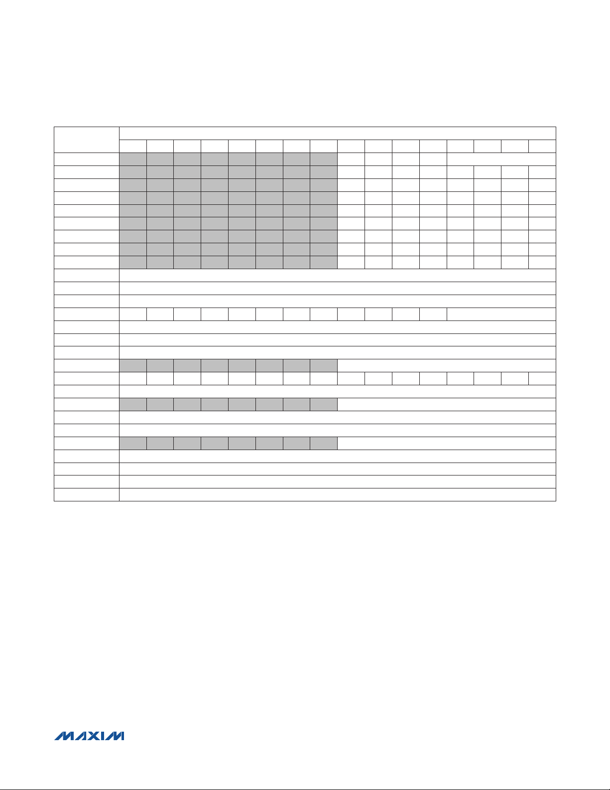
Table 3-2. System Register Bit Functions
MAX31782 User’s Guide
REGISTER
AP — — — — AP (4 bits)
APC CLR IDS — — — MOD2 MOD1 MOD0
PSF Z S — GPF1 GPF0 OV C E
IC — — — — — — INS IGE
IMR IMS — IM5 IM4 IM3 IM2 IM1 IM0
SC TAP — — CDA0 — ROD PWL —
IIR IIS — II5 II4 II3 II2 II1 II0
CKCN — — — STOP — — — —
WDCN POR EWDI WD1 WD0 WDIF WTRF EWT RWT
A[n] (n = 15:0) A[n] (16 bits)
PFX[n] (n = 7:0) PFX[n] (16 bits)
IP IP (16 bits)
SP — — — — — — — — — — — — SP (4 bits)
IV IV (16 bits)
LC[0] LC[0] (16 bits)
LC[1] LC[1] (16 bits)
OFFS OFFS (8 bits)
DPC — — — — — — — — — — — WBS2 WBS1 WBS0 SDPS1 SDPS0
GR GR (16 bits)
GRL GRL (8 bits)
BP BP (16 bits)
GRS GRS (16 bits) = (GRL:GRH)
GRH GRH (8 bits)
GRXL GRXL (16 bits) = (GRL.7, 8 bits): (GRL, 8 bits)
FP FP = BP[OFFS] (16 bits)
DP[0] DP[0] (16 bits)
DP[1] DP[1] (16 bits)
15 14 13 12 11 10 9 8 7 6 5 4 3 2 1 0
BIT
��������������������������������������������������������������� Maxim Integrated Products 3-3
Revision 0; 8/11
Page 22
MAX31782 User’s Guide
3.1 System Register Bit Descriptions
3.1.1 Accumulator Pointer Register (AP, 8h[0h])
Initialization: This register is cleared to 00h on all forms of reset.
Access: Unrestricted direct read/write access.
BIT FUNCTION
Active Accumulator Select. These bits select which of the 16 accumulator registers are used for arithmetic and
logical operations. If the APC register has been set to perform automatic increment/decrement of the active
AP.[3:0]
AP.[7:4] Reserved. All reads return 0.
3.1.2 Accumulator Pointer Control Register (APC, 8h[1h])
Initialization: This register is cleared to 00h on all forms of reset.
Access: Unrestricted direct read/write access.
BIT FUNCTION
APC.[2:0]
(MOD[2:0])
APC.[5:3] Reserved. All reads return 0.
APC.6 (IDS)
accumulator, this setting is automatically changed after each arithmetic or logical operation. If a ‘MOVE AP,
Acc’ instruction is executed, any enabled AP inc/dec/modulo control takes precedence over the transfer of Acc
data into AP.
Accumulator Pointer Auto Increment/Decrement Modulus. If these bits are set to a nonzero value, the accumulator pointer (AP[3:0]) is automatically incremented or decremented following each arithmetic or logical operation.
The mode for the auto increment/decrement is determined as follows:
MOD[2:0] AUTO INCREMENT/DECREMENT MODE
000 No auto increment/decrement (default)
001 Increment/decrement AP[0] modulo 2
010 Increment/decrement AP[1:0] modulo 4
011 Increment/decrement AP[2:0] modulo 8
100 Increment/decrement AP modulo 16
101 to 111 Reserved (modulo 16 when set)
Increment/Decrement Select. If this bit is set to 0, the accumulator pointer AP is incremented following each
arithmetic or logical operation according to MOD[2:0]. If this bit is set to 1, the accumulator pointer AP is decremented following each arithmetic or logical operation according to MOD[2:0]. If MOD[2:0] is set to 000, the setting of this bit is ignored.
APC.7 (CLR)
AP Clear. Writing this bit to 1 clears the accumulator pointer AP to 0. Once set, this bit is automatically reset to 0
by hardware. If a ‘MOVE APC, Acc’ instruction is executed requesting that AP be set to 0 (i.e., CLR = 1), the AP
clear function overrides any enabled inc/dec/modulo control. All reads from this bit return 0.
��������������������������������������������������������������� Maxim Integrated Products 3-4
Revision 0; 8/11
Page 23
MAX31782 User’s Guide
3.1.3 Processor Status Flags Register (PSF, 8h[4h])
Initialization: This register is cleared to 80h on all forms of reset.
Access: Bit 7 (Z), bit 6 (S), and bit 2 (OV) are read-only. Bits 4 and 3 (GPF1, GPF0), bit 1 (C), and bit 0 (E) are unrestricted read/write.
BIT FUNCTION
PSF.0 (E)
PSF.1 (C)
PSF.2 (OV)
PSF.3 (GPF0) General-Purpose Flag 0
PSF.4 (GPF1) General-Purpose Flag 1. These general-purpose flag bits are provided for user software control.
PSF.5 Reserved. All reads return 0.
PSF.6 (S) Sign Flag. This bit flag mirrors the current value of the high bit of the active accumulator (Acc.15).
PSF.7 (Z)
Equals Flag. This bit flag is set to 1 whenever a compare operation (CMP) returns an equal result. If a CMP
operation returns not equal, this bit is cleared.
Carry Flag. This bit flag is set to 1 whenever an add or subtract operation (ADD, ADDC, SUB, SUBB) returns a
carry or borrow. This bit flag is cleared to 0 whenever an add or subtract operation does not return a carry or
borrow. Many other instructions potentially affect the carry bit.
Overflow Flag. This flag is set to 1 if there is a carry out of bit 14 but not out of bit 15, or a carry out of bit 15 but
not out of bit 14 from the last arithmetic operation, otherwise, the OV flag remains as 0. OV indicates a negative
number resulted as the sum of two positive operands, or a positive sum resulted from two negative operands.
Zero Flag. The value of this bit flag equals 1 whenever the active accumulator is equal to zero, and it equals 0
otherwise.
3.1.4 Interrupt and Control Register (IC, 8h[5h])
Initialization: This register is cleared to 00h on all forms of reset.
Access: Unrestricted direct read/write access.
BIT FUNCTION
IC.0 (IGE)
IC.1 (INS)
IC.[7:2] Reserved. All reads return 0.
Interrupt Global Enable. This bit enables the interrupt handler if set to 1. No interrupt to the CPU is allowed if
this bit is cleared to 0.
Interrupt In Service. The INS is set by the interrupt handler automatically when an interrupt is acknowledged.
No further interrupts occur as long as the INS bit remains set. The interrupt service routine can clear the INS bit
to allow interrupt nesting. Otherwise, the INS bit is cleared automatically by the interrupt handler upon execution of an RETI/POPI instruction.
��������������������������������������������������������������� Maxim Integrated Products 3-5
Revision 0; 8/11
Page 24
MAX31782 User’s Guide
3.1.5 Interrupt Mask Register (IMR, 8h[6h])
Initialization: This register is cleared to 00h on all forms of reset.
Access: Unrestricted read/write access.
The first six bits in this register are interrupt mask bits for modules 0 to 5, one bit per module. The eighth bit, IMS, serves as a
mask for any system module interrupt sources. Setting a mask bit allows the enabled interrupt sources for the associated module
or system (for the case of IMS) to generate interrupt requests. Clearing the mask bit effectively disables all interrupt sources associated with that specific module or all system interrupt sources (for the case of IMS). The interrupt mask register is intended to
facilitate user-definable interrupt prioritization.
BIT FUNCTION
IMR.0 (IM0) Interrupt Mask for Register Module 0
IMR.1 (IM1) Interrupt Mask for Register Module 1
IMR.2 (IM2) Interrupt Mask for Register Module 2
IMR.3 (IM3) Interrupt Mask for Register Module 3
IMR.4 (IM4) Interrupt Mask for Register Module 4
IMR.5 (IM5) Interrupt Mask for Register Module 5
IMR.6 Reserved. Reads return 0.
IMR.7 (IMS) Interrupt Mask for System Modules
3.1.6 System Control Register (SC, 8h[8h])
Initialization: This register is reset to 100000s0b on all reset. Bit 1 (PWL) is set to 1 on a power-on reset only.
Access: Unrestricted read/write access.
BIT FUNCTION
SC.0 Reserved. All reads return 0.
Password Lock. This bit defaults to 1 on a power-on reset. When this bit is 1, it requires a 32-byte password to
SC.1 (PWL)
SC.2 (ROD)
SC.3 Reserved. All reads return 0.
SC.4 (CDA0)
be matched with the password in the program space before allowing access to the ROM loader’s utilities for
read/write of program memory and debug functions. Clearing this bit to 0 disables the password protection to
the ROM loader.
ROM Operation Done. This bit is used to signify completion of a ROM operation sequence to the control units.
This allows the debug engine to determine the status of a ROM sequence. Setting this bit to logic 1 causes an
internal system reset if the JTAG_SPE bit is also set. Setting the ROD bit clears the JTAG_SPE bit if it is set and
the ROD bit is automatically cleared by hardware once the control unit acknowledges the done indication.
Code Data Access Bit 0. The CDA bit is used to logically map physical program memory page to the data
space for read/write access:
CDA0 BYTE MODE ACTIVE PAGE WORD MODE ACTIVE PAGE
0 P0 P0 and P1
1 P1 P0 and P1
The logical addresses depend on which memory segment is executing. Note that CDA1 (normally at bit position SC.5) is not implemented since the maximum flash memory size is 64KB or 32KWords.
SC.[6:5] Reserved. All reads return 0.
Test Access (JTAG) Port Enable. This bit controls whether the test access port special-function pins are
SC.7 (TAP)
enabled. The TAP defaults to being enabled. Clearing this bit to 0 disables the TAP special-function pins on the
JTAG pins.
��������������������������������������������������������������� Maxim Integrated Products 3-6
Revision 0; 8/11
Page 25
MAX31782 User’s Guide
3.1.7 Interrupt Identification Register (IIR, 8h[Bh])
Initialization: This register is cleared to 00h on all forms of reset.
Access: Read-only.
The first six bits in this register indicate interrupts pending in modules 0 to 5, one bit per module. The eighth bit, IIS, indicates a
pending system interrupt, such as from the watchdog timer. The interrupt pending flags are set only for enabled interrupt sources
waiting for service. The interrupt pending flag is cleared when the pending interrupt sources within that module are disabled or
when the interrupt flags are cleared by software.
BIT FUNCTION
IIR.0 (II0) Interrupt Identifier Flag for Register Module 0
IIR.1 (II1) Interrupt Identifier Flag for Register Module 1
IIR.2 (II2) Interrupt Identifier Flag for Register Module 2
IIR.3 (II3) Interrupt Identifier Flag for Register Module 3
IIR.4 (II4) Interrupt Identifier Flag for Register Module 4
IIR.5 (II5) Interrupt Identifier Flag for Register Module 5
IIR.6 Reserved. Reads return 0.
IIR.7 (IIS) Interrupt Identifier Flag for System Modules
3.1.8 System Clock Control Register (CKCN, 8h[Eh])
Initialization: This register is cleared to 10h on all forms of reset.
Access: Unrestricted read/write access.
BIT FUNCTION
CKCN.[3:0] Reserved. All reads return 0.
Stop Mode Select. Setting this bit to 1 stops program execution and commences low-power operation. This
CKCN.4 (STOP)
CKCN.[6:5] Reserved. All reads return 0.
CKCN.7 Reserved. All reads return 1.
bit is cleared by a reset or any of the enabled external interrupts. Setting and resetting the STOP bit does not
change the system clock source and its divide ratio.
��������������������������������������������������������������� Maxim Integrated Products 3-7
Revision 0; 8/11
Page 26
MAX31782 User’s Guide
3.1.9 Watchdog Control Register (WDCN, 8h[Fh])
Initialization: Bits 5, 4, 3, and 0 are cleared to 0 on all forms of reset; for others, see individual bit descriptions.
Access: Unrestricted direct read/write access.
BIT FUNCTION
WDCN.0
(RWT)
WDCN.1
(EWT)
WDCN.2
(WTRF)
WDCN.3
(WDIF)
Reset Watchdog Timer. Setting this bit to 1 resets the watchdog timer count. If watchdog interrupt and/or reset
modes are enabled, the software must set this bit to 1 before the watchdog timer elapses to prevent an interrupt
or reset from occurring. This bit always returns 0 when read.
Enable Watchdog Timer Reset. If this bit is set to 1 when the watchdog timer elapses, the watchdog resets the
processor 512 system clock cycles later unless action is taken to disable the reset event. Clearing this bit to 0
prevents a watchdog reset from occurring but does not stop the watchdog timer or prevent watchdog interrupts
from occurring if EWDI = 1. If EWT = 0 and EWDI = 0, the watchdog timer is stopped. If the watchdog timer
is stopped (EWT = 0 and EWDI = 0), setting the EWT bit resets the watchdog interval and reset counter, and
enables the watchdog timer. This bit is cleared on power-on reset and is unaffected by other forms of reset.
Watchdog Timer Reset Flag. This bit is set to 1 when the watchdog resets the processor. Software can check this
bit following a reset to determine if the watchdog was the source of the reset. Setting this bit to 1 in software does
not cause a watchdog reset. This bit is cleared by power-on reset only and is unaffected by other forms of reset.
It should also be cleared by software following any reset so that the source of the next reset can be correctly
determined by software. This bit is only set to 1 when a watchdog reset actually occurs, so if EWT is cleared to 0
when the watchdog timer elapses, this bit is not set.
Watchdog Interrupt Flag. This bit is set to 1 when the watchdog timer interval has elapsed or can be set to 1 by
user software. When WDIF = 1, an interrupt request occurs if the watchdog interrupt has been enabled (EWDI =
1) and not otherwise masked, or prevented by an interrupt already in service (i.e., IGE = 1, IMS = 1, and INS = 0
must be true for the interrupt to occur). This bit should be cleared by software before exiting the interrupt service
routine to avoid repeated interrupts. Furthermore, if the watchdog reset has been enabled (EWT = 1), a reset is
scheduled to occur 512 system clock cycles following setting of the WDIF bit.
WDCN.4
(WD0);
WDCN.5
(WD1)
WDCN.6
(EWDI)
WDCN.7
(POR)
Watchdog Timer Mode Select Bit 0; Watchdog Timer Mode Select Bit 1. These bits determine the watchdog interval or the length of time between resetting of watchdog timer and the watchdog generated interrupt in terms of
system clocks. Modifying the watchdog interval through the WD[1:0] bits automatically resets the watchdog timer
unless the 512 system clock reset counter is already in progress, in which case, changing the WD[1:0] bits does
not affect the watchdog timer or reset counter.
WD1 WD0 CLOCKS UNTIL INTERRUPT CLOCKS UNTIL RESET
0 0 2
0 1 2
1 0 2
1 1 2
Watchdog Interrupt Enable. If this bit is set to 1, an interrupt request can be generated when the WDIF bit is set
to 1 by any means. If this bit is cleared to 0, no interrupt occurs when WDIF is set to 1; however, it does not stop
the watchdog timer or prevent watchdog resets from occurring if EWT = 1. If EWT = 0 and EWDI = 0, the watchdog timer is stopped. If the watchdog timer is stopped (EWT = 0 and EWDI = 0), setting the EWDI bit resets the
watchdog interval and reset counter, and enables the watchdog timer. This bit is cleared to 0 by power-on reset
and is unaffected by other forms of reset.
Power-On-Reset Flag. This bit is set to 1 whenever a power-on/brownout reset occurs. It is unaffected by other
forms of reset. This bit can be checked by software following a reset to determine if a power-on/brownout reset
occurred. It should always be cleared by software following a reset to ensure that the sources of following resets
can be determined correctly.
12
15
18
21
212 + 512
215 + 512
218 + 512
221 + 512
��������������������������������������������������������������� Maxim Integrated Products 3-8
Revision 0; 8/11
Page 27
MAX31782 User’s Guide
3.1.10 Accumulator n Register (A[n], 9h[nh])
Initialization: This register is cleared to 0000h on all forms of reset.
Access: Unrestricted direct read/write access.
BIT FUNCTION
A[n].[15:0]
3.1.11 Prefix Register (PFX[n], Bh[n])
Initialization: This register is cleared to 0000h on all forms of reset.
Access: Unrestricted direct read/write access.
BIT FUNCTION
PFX[n].[15:0]
This register acts as the accumulator for all ALU arithmetic and logical operations when selected by the
accumulator pointer (AP). It can also be used as a general-purpose working register.
The Prefix register provides a means of supplying an additional 8 bits of high-order data for use by the
succeeding instruction as well as providing additional indexing capabilities. This register only holds any
data written to it for one execution cycle, after which it reverts to 0000h. Although this is a 16-bit register,
only the lower 8 bits are actually used for prefixing purposes by the next instruction. Writing to or reading
from any index in the prefix module selects the same 16-bit register. However, when the PFX register is
written, the index n used for the PFX[n] write also determines the high-order bits for the register source
and destination specified in the following instruction.
WRITE TO
PFX[0] 0h to Fh 0h to 7h
PFX[1] 10h to 1Fh 0h to 7h
PFX[2] 0h to Fh 8h to Fh
PFX[3] 10h to 1Fh 8h to Fh
PFX[4] 0h to Fh 10h to 17h
PFX[5] 10h to 1Fh 10h to 17h
PFX[6] 0h to Fh 18h to 1Fh
PFX[7] 10h to 1Fh 18h to 1Fh
The index selection reverts to 0 (default mode allowing selection of registers 0h to 7h for destinations)
after one cycle in the same manner as the contents of the PFX register.
SOURCE REGISTER RANGE DESTINATION REGISTER RANGE
SOURCE, DESTINATION INDEX SELECTION
3.1.12 Instruction Pointer Register (IP, Ch[0h])
Initialization: This register is cleared to 8000h on all forms of reset.
Access: Unrestricted direct read/write access.
BIT FUNCTION
This register contains the address of the next instruction to be executed and is automatically incremented
IP.[15:0]
by 1 after each program fetch. Writing an address value to this register caused program flow to jump to
that address. Reading from this register does not affect program flow.
��������������������������������������������������������������� Maxim Integrated Products 3-9
Revision 0; 8/11
Page 28
MAX31782 User’s Guide
3.1.13 Stack Pointer Register (SP, Dh[1h])
Initialization: This register is cleared to 000Fh on all forms of reset.
Access: Unrestricted direct read/write access.
BIT FUNCTION
SP.[3:0]
SP.[15:4] Reserved. All reads return 0.
3.1.14 Interrupt Vector Register (IV, Dh[2h])
Initialization: This register is cleared to 0000h on all forms of reset.
Access: Unrestricted direct read/write access.
BIT FUNCTION
IV.[15:0]
3.1.15 Loop Counter 0 Register (LC[0], Dh[6h])
Initialization: This register is cleared to 0000h on all forms of reset.
Access: Unrestricted direct read/write access.
BIT FUNCTION
LC[0].[15:0]
These four bits indicate the current top of the hardware stack, from 0h to Fh. This pointer is incremented
after a value is pushed on the stack and decremented before a value is popped from the stack.
This register contains the address of the interrupt service routine. The interrupt handler generates a CALL
to this address whenever an interrupt is acknowledged.
This register is used as the loop counter for the DJNZ LC[0], src operation. This operation decrements
LC[0] by one and then jumps to the address specified in the instruction by src.
3.1.16 Loop Counter 1 Register (LC[1], Dh[7h])
Initialization: This register is cleared to 0000h on all forms of reset.
Access: Unrestricted direct read/write access.
BIT FUNCTION
LC[1].[15:0]
This register is used as the loop counter for the DJNZ LC[1], src operation. This operation decrements
LC[1] by one and then jumps to the address specified in the instruction by src.
3.1.17 Frame Pointer Offset Register (OFFS, Eh[3h])
Initialization: This register is cleared to 00h on all forms of reset.
Access: Unrestricted direct read/write access.
BIT FUNCTION
This 8-bit register provides the Frame Pointer (FP) offset from the base pointer (BP). The Frame Pointer is
formed by unsigned addition of Frame Pointer Base register (BP) and Frame Pointer Offset register (OFFS).
OFFS.[7:0]
The contents of this register can be postincremented or postdecremented when using the Frame Pointer
for read operations and can be preincremented or predecremented when using the Frame Pointer for write
operations. A carry out or borrow resulting from an increment/decrement operation has no affect on the
Frame Pointer Base register (BP).
�������������������������������������������������������������� Maxim Integrated Products 3-10
Revision 0; 8/11
Page 29
MAX31782 User’s Guide
3.1.18 Data Pointer Control Register (DPC, Eh[4h])
Initialization: This register is cleared to 001Ch on all forms of reset.
Access: Unrestricted direct read/write access.
BIT FUNCTION
Source Data Pointer Select Bits 1:0. These bits select one of the three data pointers as the active source pointer for the load operation. A new data pointer must be selected before being used to read data memory:
SDPS1 SDPS0 SOURCE POINTER SELECTION
0 0 DP[0]
DPC.[1:0]
(SDPS[1:0])
These bits default to 00b but do not activate DP[0] as an active source pointer until the SDPS bits are explicitly
cleared to 00b or the DP[0] register is written by an instruction. Also, modifying the register contents of a data/
frame pointer register (DP[0], DP[1], BP, or OFFS) changes the setting of the SDPS bits to reflect the active
source pointer selection.
Word/Byte Select 0. This bit selects access mode for DP[0]. When WBS0 is set to logic 1, the DP[0] is oper-
DPC.2 (WBS0)
DPC.3 (WBS1)
DPC.4 (WBS2)
DPC.[15:5] Reserved. Read returns 0.
ated in word mode for data memory access; when WBS0 is cleared to logic 0, DP[0] is operated in byte mode
for data memory access.
Word/Byte Select 1. This bit selects access mode for DP[1]. When WBS1 is set to logic 1, the DP[1] is operated in word mode for data memory access; when WBS1 is cleared to logic 0, DP[1] is operated in byte mode
for data memory access.
Word/Byte Select 2. This bit selects access mode for BP[OFFS]. When WBS2 is set to logic 1, the BP[OFFS]
is operated in word mode for data memory access; when WBS2 is cleared to logic 0, BP[OFFS] is operated in
byte mode for data memory access.
0 1 DP[1]
1 0 FP (BP[OFFS])
1 1 Reserved (select FP if set)
3.1.19 General Register (GR, Eh[5h])
Initialization: This register is cleared to 0000h on all forms of reset.
Access: Unrestricted direct read/write access.
BIT FUNCTION
This register is intended primarily for supporting byte operations on 16-bit data. The 16-bit register is byte-
GR.[15:0]
readable, byte-writable through the corresponding GRL and GRH 8-bit registers and byte-swappable through
the GRS 16-bit register.
3.1.20 General Register Low Byte (GRL, Eh[6h])
Initialization: This register is cleared to 00h on all forms of reset.
Access: Unrestricted direct read/write access.
BIT FUNCTION
GRL.[7:0]
This register reflects the low byte of the GR register and is intended primarily for supporting byte operations
on 16-bit data. Any data written to the GRL register is also stored in the low byte of the GR register.
�������������������������������������������������������������� Maxim Integrated Products 3-11
Revision 0; 8/11
Page 30
MAX31782 User’s Guide
3.1.21 Frame Pointer Base Register (BP, Eh[7h])
Initialization: This register is cleared to 0000h on all forms of reset.
Access: Unrestricted direct read/write access.
BIT FUNCTION
This register serves as the base pointer for the frame pointer (FP). The frame pointer is formed by unsigned addi-
BP.[15:0]
3.1.22 General Register Byte-Swapped (GRS, Eh[8h])
Initialization: This register is cleared to 0000h on all forms of reset.
Access: Unrestricted read-only access.
BIT FUNCTION
GRS.[15:0]
3.1.23 General Register High Byte (GRH, Eh[9h])
Initialization: This register is cleared to 00h on all forms of reset.
Access: Unrestricted direct read/write access.
BIT FUNCTION
GRH.[7:0]
tion of frame pointer base register (BP) and frame pointer offset register (OFFS). The content of this base pointer
register is not affected by increment/decrement operations performed on the offset (OFFS) register.
This register is intended primarily for supporting byte operations on 16-bit data. This 16-bit read-only register returns the byte-swapped value for the data contained in the GR register.
This register reflects the high byte of the GR register and is intended primarily for supporting byte operations
on 16-bit data. Any data written to the GRH register is also stored in the high byte of the GR register.
3.1.24 General Register Sign Extended Low Byte (GRXL, Eh[Ah])
Initialization: This register is cleared to 0000h on all forms of reset.
Access: Unrestricted direct read-only access.
BIT FUNCTION
GRXL.[15:0] This register provides the sign extended low byte of GR as a 16-bit source.
3.1.25 Frame Pointer Register (FP, Eh[Bh])
Initialization: This register is cleared to 0000h on all forms of reset.
Access: Unrestricted direct read-only access.
BIT FUNCTION
FP.[15:0] This register provides the current value of the frame pointer (BP[OFFS]).
3.1.26 Data Pointer 0 Register (DP[0], Fh[3h])
Initialization: This register is cleared to 0000h on all forms of reset.
Access: Unrestricted direct read/write access.
BIT FUNCTION
This register is used as a pointer to access data memory. DP[0] can be automatically incremented or dec-
DP[0].[15:0]
remented following each read operation, or can be automatically incremented or decremented before each
write operation.
�������������������������������������������������������������� Maxim Integrated Products 3-12
Revision 0; 8/11
Page 31

MAX31782 User’s Guide
3.1.27 Data Pointer 1 Register (DP[1], Fh[7h])
Initialization: This register is cleared to 0000h on all forms of reset.
Access: Unrestricted direct read/write access.
BIT FUNCTION
This register is used as a pointer to access data memory. DP[1] can be automatically incremented or dec-
DP[1].[15:0]
remented following each read operation, or can be automatically incremented or decremented before each
write operation.
�������������������������������������������������������������� Maxim Integrated Products 3-13
Revision 0; 8/11
Page 32

MAX31782 User’s Guide
SECTION 4: PERIPHERAL REGISTER MODULES
The MAX31782 has six peripheral register modules, Modules 0 through 5. This section describes the MAX31782’s
peripheral registers. Table 4-1 shows the MAX31782 peripheral register map. Table 4-2 explains peripheral register bit
functions. Detailed peripheral register bit descriptions and default values appear in the corresponding function block
description section.
Table 4-1. Peripheral Register Map
INDEX M0 M1 M2 M3 M4 M5
00h PO2 I2CBUF_M I2CBUF_S PWMC0 PWMC2 MCNT
01h PO1 I2CST_M I2CST_S PWMR0 PWMR2 MA
02h I2CIE_M I2CIE_S PWMC1 PWMC3 MB
03h MIIR0 PO6 MIIR2 PWMR1 PWMR3 MC2
04h MIIR1 SMBUS MC1
05h TACHR0 TACHR2 MC0
06h TB0C EIF6 ADST MC1R
07h TB0R EIE6 ADADDR TACHR1 TACHR3 MC0R
08h PI2 PI6 ADCN PWMV0 PWMV2 PWMV4
09h PI1 SVM ADDATA PWMCN0 PWMCN2 PWMCN4
0Ah PWMV1 PWMV3 PWMC4
0Bh TB0V PWMCN1 PWMCN3 PWMR4
0Ch I2CCN_M I2CCN_S TACHV0 TACHV2 TACHV4
0Dh TB0CN I2CCK_M I2CCK_S TACHCN0 TACHCN2 TACHCN4
0Eh I2CTO_M I2CTO_S TACHV1 TACHV3
0Fh I2CSLA_M I2CSLA_S TACHCN1 TACHCN3 TACHR4
10h PD2 EIES6 MIIR3 MIIR4
11h PD1 TACHR5
12h PD6 TACHV5
13h TACHCN5
14h PWMC5
15h I2C_SPB PWMR5
16h ETS DEV_NUM PWMV5
17h ADCG1 PWMCN5
18h ADCG5 ICDT0 MIIR5
19h ADVOFF ICDT1
1Ah TOEX ICDC
1Bh ICDF
1Ch ICDB
1Dh ICDA
1Eh ICDD
1Fh
��������������������������������������������������������������� Maxim Integrated Products 4-1
Revision 0; 8/11
Page 33

MAX31782 User’s Guide
TB0
CP/RLB
I2CAMI I2CTOI I2CSTRI I2CRXI I2CTXI I2CSRI
—
I2CAMIE I2CTOIE I2CSTRIE I2CRXIE I2CTXIE I2CSRIE
—
SVMSTOP SVMI SVMIE SVMRDY SVMEN
— — —
EXTERNAL TEMP SLOPE [7:0]
— A[6:0]
MODULE 0
PO2 00h PO2[7:0]
PO1 01h — — PO1[5:0]
REGISTER INDEX 15 14 13 12 11 10 9 8 7 6 5 4 3 2 1 0
Table 4-2. Peripheral Register Bit Functions
— — — — — — — — — — — — — —
MIIR0 03h —
PI2 08h PI2[7:0]
TB0R 07h TB0R[15:0]
TB0C 06h TB0C[15:0]
PI1 09h — — PI1[5:0]
TB0V 0Bh TB0V[15:0]
— —
TBCS TBCR TBPS[2:0] TFB EXFB TBOE DCEN EXENB TRB ETB
C/TB
TB0CN 0Dh
PD2 10h PD2[7:0]
PD1 11h — — PD1[5:0]
MODULE 1
I2CM_WU I2CM P6_7 P6_6 SVM P6_4 P6_3 P6_2 P6_1 P6_0
SVMTH[3:0]
PI6 08h PI6_7 PI6_6 — PI6_4 PI6_3 PI6_2 PI6_1 PI6_0
— — — —
SVM 09h
— — I2CSTREN I2CGCEN I2CSTOP I2CSTART I2CACK I2CSTRS — I2CMODE I2CMST I2CEN
— — — —
I2CCN_M 0Ch
— — — — — — —
I2CTO_M 0Eh I2CTO[7:0]
I2CCK_M 0Dh I2CCKH[7:0] I2CCKL[7:0]
I2CSLA_M 0Fh —
PD6 12h PD6[7:0]
EIES6 10h IESP6_7 IESP6_7 — IESP6_4 IESP6_3 IESP6_2 IESP6_1 IESP6_0
— — — — — — — —
ETS 16h
ADCG1 17h — ADC VOLTAGE SCALE TRIM FOR GAIN 1 [14:0]
ADCG5 18h — ADC VOLTAGE SCALE TRIM FOR GAIN 5 [14:0]
ADVOFF 19h ADC VOLTAGE OFFSET [15:0]
TOEX 1Ah EXTERNAL TEMP OFFSET [15:0]
-— — — — D[7:0]
I2CSPI I2CSCL I2CROI I2CGCI I2CNACKI
I2CSPIE — I2CROIE I2CGCIE I2CNACKIE
— —
— —
— — — — — —
— — — —
PO6 03h PO6_7 PO6_6 — PO6_4 PO6_3 PO6_2 PO6_1 PO6_0
EIF6 06h IFP6_7 IFP6_6 — IFP6_4 IFP6_3 IFP6_2 IFP6_1 IFP6_0
EIE6 07h IEP6_7 IEP6_7 — IEP6_4 IEP6_3 IEP6_2 IEP6_1 IEP6_0
MIIR1 04h
I2CIE_M 02h
I2CST_M 01h I2CBUS I2CBUSY
I2CBUF_M 00h — —
REGISTER INDEX 15 14 13 12 11 10 9 8 7 6 5 4 3 2 1 0
��������������������������������������������������������������� Maxim Integrated Products 4-2
Revision 0; 8/11
Page 34

A[6:0]
I2C_SPE
— — PSS1 PSS0 JTAG_SPE TXC
MAX31782 User’s Guide
TACH1 TACH0
TEXEN TACHE TACHIE —
RESET_S RESET_M SMB_MOD_S SMB_MOD_M
DCEN — PWMEN ETB —
DCEN — PWMEN ETB —
— —
— —
TEXEN TACHE TACHIE —
— —
— —
— —
MODULE 2
— — — — — — — I2CS_WU I2CS ADC
— — — — D[7:0]
— —
I2CSPI I2CSCL I2CROI I2CGCI I2CNACKI — I2CAMI I2CTOI I2CSTRI I2CRXI I2CTXI I2CSRI
— —
I2CROIE I2CGCIE I2CNACKIE — I2CAMIE I2CTOIE I2CSTRIE I2CRXIE I2CTXIE I2CSRIE
—
—
I2CSPIE
— — — —
— — — —
ADDAT[3:0] — ADCONV ADDAI ADCFG ADIDX[3:0]
—
— — — —
ADBADD[3:0] — ADSTART[2:0] — ADEND[2:0]
— — — —
I2CSTREN I2CGCEN I2CSTOP I2CSTART I2CACK I2CSTRS — I2CMODE I2CMST I2CEN
— — — — — —
— — — — — — — — —
— — — — — — — — — — — — — — —
MODULE 3
TPS[2:0] TF TEXF
PWMCS PWMCR PWMPS[2:0] TFB
— — — — — — — — — — —
— — —
— —
PWMCS PWMCR PWMPS[2:0] TFB
— — —
— — — — — — — — — — — — — —
I2CST_S 01h I2CBUS I2CBUSY
I2CBUF_S 00h — —
REGISTER INDEX 15 14 13 12 11 10 9 8 7 6 5 4 3 2 1 0
Table 4-2. Peripheral Register Bit Functions (continued)
I2CIE_S 02h
MIIR2 03h
ADST 06h
ADCN 08h — ADCCLK[2:0] ADDAINV[1:0] — — IREFEN ADCONT ADDAIE — ADACQ[3:0]
ADADDR 07h
ADDATA 09h ADDATA[15:0], SEE SECTION 6: Analog-to-Digital Converter (ADC) FOR DETAILS
I2CCN_S 0Ch
I2CTO_S 0Eh I2CTO[7:0]
I2CCK_S 0Dh I2CCKH[7:0] I2CCKL[7:0]
I2CSLA_S 0Fh
I2C_SPB 15h
DEV_NUM 16h DEVICE NUMBER[7:0]
ICDC 1Ah DME — REGE — CMD[3:0]
ICDT0 18h ICDT0[15:0]
ICDT1 19h ICDT1[15:0]
ICDF 1Bh
ICDB 1Ch ICDB[7:0]
ICDA 1Dh ICDA[15:0]
ICDD 1Eh ICDD[15:0]
PWMC0 00h PWMC0[15:0]
REGISTER INDEX 15 14 13 12 11 10 9 8 7 6 5 4 3 2 1 0
PWMR0 01h PWMR0[15:0]
PWMR1 03h PWMR1[15:0]
PWMC1 02h PWMC1[15:0]
SMBUS 04h —
TACHR0 05h TACHR0[15:0]
PWMV0 08h PWMV0[15:0]
TACHR1 07h TACHR1[15:0]
PWMCN0 09h
PWMV1 0Ah PWMV1[15:0]
TACHV0 0Ch TACHV0[15:0]
PWMCN1 0Bh
TACHCN0 0Dh — TRPS[1:0]
MIIR3 10h
TACHV1 0Eh TACHV1[15:0]
TACHCN1 0Fh — TRPS[1:0] — — TPS[2:0] TF TEXF
��������������������������������������������������������������� Maxim Integrated Products 4-3
Revision 0; 8/11
Page 35

MAX31782 User’s Guide
TACH3 TACH2
MODULE 4
MODULE 5
TACH5 TACH4
PWMR2 01h PWMR2[15:0]
PWMC2 00h PWMC2[15:0]
REGISTER INDEX 15 14 13 12 11 10 9 8 7 6 5 4 3 2 1 0
Table 4-2. Peripheral Register Bit Functions (continued)
— — — — — — — — —
PWMCS PWMCR PWMPS[2:0] TFB — — DCEN — PWMEN ETB —
— — —
— — — — — — — — — — — — — —
MA 01h MA[15:0]
MB 02h MB[15:0]
MC2 03h MC2[15:0]
MC1 04h MC1[15:0]
PWMR3 03h PWMR3[15:0]
PWMC3 02h PWMC3[15:0]
TACHR2 05h TACHR2[15:0]
PWMV2 08h PWMV2[15:0]
TACHR3 07h TACHR3[15:0]
PWMCN2 09h — — — PWMCS PWMCR PWMPS[2:0] TFB — — DCEN — PWMEN ETB —
PWMV3 0Ah PWMV3[15:0]
TACHV2 0Ch TACHV2[15:0]
PWMCN3 0Bh — — — PWMCS PWMCR PWMPS[2:0] TFB — — DCEN — PWMEN ETB —
TACHV3 0Eh TACHV3[15:0]
TACHCN2 0Dh — TRPS[1:0] — — TPS[2:0] TF TEXF — — TEXEN TACHE TACHIE —
MIIR4 10h — — — — —
TACHCN3 0Fh — TRPS[1:0] — — TPS[2:0] TF TEXF — — TEXEN TACHE TACHIE —
MCNT 00h OF MCW CLD SQU OPCS MSUB MMAC SUS
REGISTER INDEX 15 14 13 12 11 10 9 8 7 6 5 4 3 2 1 0
MC0 05h MC0[15:0]
MC1R 06h MC1R[15:0]
MC0R 07h MC0R[15:0]
PWMV4 08h PWMV4[15:0]
PWMCN4 09h — — — PWMCS PWMCR PWMPS[2:0] TFB — — DCEN — PWMEN ETB —
PWMR4 0Bh PWMR4[15:0]
PWMC4 0Ah PWMC4[15:0]
TACHV4 0Ch TACHV4[15:0]
TACHR4 0Fh TACHR4[15:0]
TACHCN4 0Dh — TRPS[1:0] — — TPS[2:0] TF TEXF — — TEXEN TACHE TACHIE —
TACHV5 12h TACHV5[15:0]
TACHR5 11h TACHR5[15:0]
TACHCN5 13h — TRPS[1:0] — — TPS[2:0] TF TEXF — — TEXEN TACHE TACHIE —
PWMV5 16h PWMV5[15:0]
PWMR5 15h PWMR5[15:0]
PWMC5 14h PWMC5[15:0]
PWMCN5 17h
��������������������������������������������������������������� Maxim Integrated Products 4-4
Revision 0; 8/11
MIIR5 18h
Page 36

MAX31782 User’s Guide
SECTION 5: INTERRUPTS
This section contains the following information:
5.1 Servicing Interrupts . . . . . . . . . . . . . . . . . . . . . . . . . . . . . . . . . . . . . . . . . . . . . . . . . . . . . . . . . . . . . . . . . . . . . . . .5-2
5.2 Module Interrupt Identification Registers. . . . . . . . . . . . . . . . . . . . . . . . . . . . . . . . . . . . . . . . . . . . . . . . . . . . . . . .5-5
5.2.1 Peripheral Module 0 Interrupt Identification Register (MIIR0, M0[03h]) . . . . . . . . . . . . . . . . . . . . . . . . . . .5-5
5.2.2 Peripheral Module 1 Interrupt Identification Register (MIIR1, M1[04h]) . . . . . . . . . . . . . . . . . . . . . . . . . . .5-5
5.2.3 Peripheral Module 2 Interrupt Identification Register (MIIR2, M2[03h]) . . . . . . . . . . . . . . . . . . . . . . . . . . .5-6
5.2.4 Peripheral Module 3 Interrupt Identification Register (MIIR3, M3[10h]) . . . . . . . . . . . . . . . . . . . . . . . . . . .5-6
5.2.5 Peripheral Module 4 Interrupt Identification Register (MIIR4, M4[10h]) . . . . . . . . . . . . . . . . . . . . . . . . . . .5-6
5.2.6 Peripheral Module 5 Interrupt Identification Register (MIIR5, M5[18h]) . . . . . . . . . . . . . . . . . . . . . . . . . . .5-7
5.3 Interrupt System Operation . . . . . . . . . . . . . . . . . . . . . . . . . . . . . . . . . . . . . . . . . . . . . . . . . . . . . . . . . . . . . . . . . .5-7
5.3.1 Synchronous vs. Asynchronous Interrupt Sources . . . . . . . . . . . . . . . . . . . . . . . . . . . . . . . . . . . . . . . . . . .5-7
5.3.2 Interrupt Prioritization by Software . . . . . . . . . . . . . . . . . . . . . . . . . . . . . . . . . . . . . . . . . . . . . . . . . . . . . . . .5-8
5.3.3 Interrupt Exception Window . . . . . . . . . . . . . . . . . . . . . . . . . . . . . . . . . . . . . . . . . . . . . . . . . . . . . . . . . . . . .5-8
LIST OF FIGURES
Figure 5-1. Interrupt Hierarchy. . . . . . . . . . . . . . . . . . . . . . . . . . . . . . . . . . . . . . . . . . . . . . . . . . . . . . . . . . . . . . . . . . .5-3
LIST OF TABLES
Table 5-1. Interrupt Sources and Control Bits . . . . . . . . . . . . . . . . . . . . . . . . . . . . . . . . . . . . . . . . . . . . . . . . . . . . . . .5-4
��������������������������������������������������������������� Maxim Integrated Products 5-1
Revision 0; 8/11
Page 37

MAX31782 User’s Guide
SECTION 5: INTERRUPTS
The MAX31782 provides a single, programmable interrupt vector (IV) that can be used to handle internal and external
interrupts. Interrupts can be generated from system level sources (e.g., watchdog timer) or by sources associated with
the peripheral modules. Only one interrupt can be handled at a time, and all interrupts naturally have the same priority.
A programmable interrupt mask register (IMR) allows software-controlled prioritization and nesting of high-priority interrupts. Figure 5-1 shows a diagram of the interrupt hierarchy.
5.1 Servicing Interrupts
For the MAX31782 to service an interrupt, interrupts must be enabled globally, modularly, and locally. The interrupt
global enable (IGE) bit located in the interrupt and control (IC) register acts as a global interrupt mask. This bit defaults
to 0, and it must be set to 1 before any interrupt takes place.
The local interrupt-enable bit for a particular source is in one of the peripheral registers associated with that peripheral
module, or in a system register for any system interrupt source. Between the global and local enables are intermediate per-module and system interrupt mask bits. These mask bits reside in the interrupt mask system register (IMR).
By implementing intermediate per-module masking capability in a single register, interrupt sources spanning multiple
modules can be selectively enabled/disabled in a single instruction. This promotes a simple, fast, and user-definable
interrupt prioritization scheme. The interrupt source-enable hierarchy is illustrated in Figure 5-1 as well as Table 5-1.
When an interrupt condition occurs, its individual flag is set, even if the interrupt source is disabled at the local, module,
or global level. Interrupt flags must be cleared within the user interrupt routine to avoid repeated interrupts from the
same source.
Since all interrupts vector to the address contained in the interrupt vector register (IV), the interrupt identification register (IIR) can be used by the interrupt service routine to determine the module source of an interrupt. The IIR register
contains a bit flag for each peripheral module and one flag associated with all system interrupts; if the bit for a module
is set, then an interrupt is pending that was initiated by that module.
The MAX31782 provides two ways to determine which block inside a module caused an interrupt to occur. Each module
has a module interrupt identification register (MIIR) that indicates which of the module’s interrupt sources has a pending interrupt. The peripheral register bits inside the module also provide a way to differentiate among interrupt sources.
Section 5.2 Module Interrupt Identification Registers has more detail on the MIIR registers.
The IV register provides the location of the interrupt service routine. It can be set to any location within program memory.
The IV register defaults to 0000h on reset or power-up, so if it is not changed to a different address, the user program
must determine whether a jump to 0000h came from a reset or interrupt source.
��������������������������������������������������������������� Maxim Integrated Products 5-2
Revision 0; 8/11
Page 38

SYSTEM MODULE
WATCHDOG INTERRUPTS
WDCN.WDIF
WDCN.EWDI (LOCAL ENABLE)
MODULE 1
GPIO INTERRUPTS
EXTERNAL INTERRUPT P6.0: EIF6.IFP6_0
LOCAL ENABLE EIE6.IEP6_0
EXTERNAL INTERRUPT P6.n: EIF6.IFP6_n
LOCAL ENABLE EIE6.IEP6_n
2
MASTER I
MASTER I2C START INTERRUPT I2CST_M.I2CSRI
LOCAL ENABLE I2CIE_M.I2CSRIE
ANY I2C INTERRUPT I2CST_M.x
C INTERRUPTS
LOCAL ENABLE I2CIE_M.x
SVM INTERRUPTS
SVM INTERRUPT SVM.SVMI
LOCAL ENABLE SVM.SVMIE
MODULE 0
TIMER B INTERRUPTS
EXTERNAL TRIGGER TB0CN.EXFB
LOCAL ENABLE TB0CN.ETB
OVERFLOW TB0CN.TFB
LOCAL ENABLE TB0CN.ETB
MAX31782 User’s Guide
IIR.IIS
IMR.IMS
MODULE ENABLE
IIR.II1
IMR.IM1
MODULE 1 ENABLE
IC.INS
INTERRUPT IS NOT
IN SERVICE
JUMP TO
INTERRUPT
VECTOR
IC.IGE
GLOBAL ENABLE
IIR.II0
IMR.IM0
MODULE 0 ENABLE
MODULE 3
TACHOMETER 0 INTERRUPTS
OVERFLOW TACHCN0.TF
LOCAL ENABLE TACHCN0.TACHIE
EDGE TRIGGER TACHCN0.TEXF
LOCAL ENABLE TACHCN0.TACHIE
TACHOMETER 1 INTERRUPTS
OVERFLOW TACHCN1.TF
LOCAL ENABLE TACHCN1.TACHIE
EDGE TRIGGER TACHCN1.TEXF
LOCAL ENABLE TACHCN1.TACHIE
NOTE: ONLY A FEW OF THE MAX31782 MODULES AND INTERRUPT SOURCES ARE SHOWN IN THIS INTERRUPT HIERARCHY FIGURE. REFER TO THE CORRESPONDING
SECTIONS OF THIS USER’S GUIDE FOR MORE DETAILED INFORMATION ABOUT ALL THE POSSIBLE INTERRUPTS.
MODULE 3 ENABLE
IIR.II3
IMR.IM3
Figure 5-1. Interrupt Hierarchy
��������������������������������������������������������������� Maxim Integrated Products 5-3
Revision 0; 8/11
Page 39

Table 5-1. Interrupt Sources and Control Bits
MAX31782 User’s Guide
MODULE
INTERRUPT INTERRUPT FLAG LOCAL ENABLE BIT
Timer B: External Trigger TB0CN.EXFB
Timer B: Overflow TB0CN.TFB
I2C Master START Interrupt I2CST_M.I2CSRI I2CIE_M.I2CSRIE
I2C Master Transmit Complete Interrupt I2CST_M.I2CTXI I2CIE_M.I2CTXIE
I2C Master Receive Ready Interrupt I2CST_M. I2CRXI I2CIE_M.I2CRXIE
I2C Master Clock Stretch Interrupt I2CST_M.I2CSTRI I2CIE_M.I2CSTRIE
I2C Master Timeout Interrupt I2CST_M.I2CTOI I2CIE_M.I2CTOIE
I2C Master NACK Interrupt I2CST_M.I2CNACKI I2CIE_M.I2CNACKIE
I2C Master Receiver Overrun Interrupt I2CST_M.I2CROI I2CIE_M.I2CROIE
I2C Master STOP Interrupt I2CST_M.I2CSPI I2CIE_M.I2CSPIE
I2C Master Wake-Up Interrupt I2CST_M.I2CSRI I2CIE_M.I2CSRIE MIIR1.I2CM_WU
External Interrupt P6.0 EIF6.IFP6_0 EIE6.IEP6_0 MIIR1.P6_0
External Interrupt P6.1 EIF6.IFP6_1 EIE6.IEP6_1 MIIR1.P6_1
External Interrupt P6.2 EIF6.IFP6_2 EIE6.IEP6_2 MIIR1. P6_2
External Interrupt P6.3 EIF6.IFP6_3 EIE6.IEP6_3 MIIR1. P6_3
External Interrupt P6.4 EIF6.IFP6_4 EIE6.IEP6_4 MIIR1. P6_4
External Interrupt P6.6 EIF6.IFP6_6 EIE6.IEP6_6 MIIR1. P6_6
External Interrupt P6.7 EIF6.IFP6_7 EIE6.IEP6_7 MIIR1. P6_7
Supply Voltage Monitor Interrupt SVM.SVMI SVM.SVMIE MIIR1.SVM
I2C Slave START Interrupt I2CST_S.I2CSRI I2CIE_S.I2CSRIE
I2C Slave Transmit Complete Interrupt I2CST_S.I2CTXI I2CIE_S.I2CTXIE
I2C Slave Receive Ready Interrupt I2CST_S. I2CRXI I2CIE_S.I2CRXIE
I2C Slave Clock Stretch Interrupt I2CST_S.I2CSTRI I2CIE_S.I2CSTRIE
I2C Slave Timeout Interrupt I2CST_S.I2CTOI I2CIE_S.I2CTOIE
I2C Slave Address Match Interrupt I2CST_S.I2CAMI I2CIE_S.I2CAMIE
I2C Slave NACK Interrupt I2CST_S.I2CNACKI I2CIE_S.I2CNACKIE
I2C Slave General Call Interrupt I2ST_S.I2CGCI I2CIE_S.I2CGCIE
I2C Slave Receiver Overrun Interrupt I2CST_S.I2CROI I2CIE_S.I2CROIE
I2C Slave STOP Interrupt I2CST_S.I2CSPI I2CIE_S.I2CSPIE
I2C Slave Wake-Up Interrupt I2CST_S.I2CSRI I2CIE_S.I2CSRIE MIIR2.I2CS_WU
ADC Data Available Interrupt ADST.ADDAI ADCN.ADDAIE MIIR2.ADC
TACH.0 Overflow TACHCN0.TF
External TACH.0 Trigger TACHCN0.TEXF
TACH.1 Overflow TACHCN1.TF
External TACH.1 Trigger TACHCN1.TEXF
TACH.2 Overflow TACHCN2.TF
External TACH.2 Trigger TACHCN2.TEXF
TACH.3 Overflow TACHCN3.TF
External TACH.3 Trigger TACHCN3.TEXF
TACH.4 Overflow TACHCN4.TF
External TACH.4 Trigger TACHCN4.TEXF
TACH.5 Overflow TACHCN5.TF
External TACH.5 Trigger TACHCN5.TEXF
Watchdog Interrupt WDCN.WDIF WDCN.EWDI N/A IIR.IIS IMR.IMS
TB0CN.ETB MIIR0.TB0 IIR.II0 IMR.IM0
TACHCN0.TACHIE MIIR3.TACH0
TACHCN1.TACHIE MIIR3.TACH1
TACHCN2.TACHIE MIIR4.TACH2
TACHCN3.TACHIE MIIR4.TACH3
TACHCN4.TACHIE MIIR5.TACH4
TACHCN5.TACHIE MIIR5.TACH5
INTERRUPT
IDENTIFICATION
BIT
MIIR1.I2CM
MIIR2.I2CS
INTERRUPT
IDENTIFICATION
BIT
IIR.II1 IMR.IM1
IIR.II2 IMR.IM2
IIR.II3 IMR.IM3
IIR.II4 IMR.IM4
IIR.II5 IMR.IM5
MODULE
ENABLE
BIT
��������������������������������������������������������������� Maxim Integrated Products 5-4
Revision 0; 8/11
Page 40

MAX31782 User’s Guide
5.2 Module Interrupt Identification Registers
The MIIR registers are implemented to indicate which particular function within a peripheral module has caused the
interrupt. The MAX31782 has six peripheral modules, M0 to M5. An MIIR register is implemented in each peripheral
module. The MIIR registers are 16-bit read-only registers and all of them default to 0000h on system reset.
Each defined bit in an MIIR register is the final interrupt from a specific function, i.e., the interrupt enable bit(s) ANDed
with the interrupt flag(s). A function can have multiple flags, but they all are ANDed with corresponding enable bits and
combined to create a single interrupt identification bit for that specific function. For example, the I2C master has several
interrupt sources; however, they all are combined to form a single identification bit, MIIR1.I2CM. The individual register
bit functions are defined as follows.
5.2.1 Peripheral Module 0 Interrupt Identification Register (MIIR0, M0[03h])
Bit
Name — — — — — — — — — — — — — — — TB0
Reset 0 0 0 0 0 0 0 0 0 0 0 0 0 0 0 0
Access r r r r r r r r r r r r r r r r
15 14 13 12 11 10 9 8 7 6 5 4 3 2 1 0
BIT NAME DESCRIPTION
15:1 — Reserved. A read returns 0.
0 TB0 This bit is set when an interrupt is generated by the Timer/Counter B module.
5.2.2 Peripheral Module 1 Interrupt Identification Register (MIIR1, M1[04h])
Bit
Name — — — — — — I2CM_WU I2CM P6_7 P6_6 SVM P6_4 P6_3 P6_2 P6_1 P6_0
Reset 0 0 0 0 0 0 0 0 0 0 0 0 0 0 0 0
Access r r r r r r r r r r r r r r r r
15 14 13 12 11 10 9 8 7 6 5 4 3 2 1 0
BIT NAME DESCRIPTION
15:10 — Reserved. A read returns 0.
This bit is set when there is a wake-up interrupt from the I2C master block. For this to occur, the I2C
9 I2CM_WU
8 I2CM
7 P6_7 This bit is set when there is an external GPIO Interrupt at P6.7 (slave I2C SDA).
6 P6_6 This bit is set when there is an external GPIO Interrupt at P6.6 (slave I2C SCL).
5 SVM This bit is set when there is an interrupt from supply voltage monitor (SVM).
4 P6_4 This bit is set when there is an external interrupt at P6.4.
3 P6_3 This bit is set when there is an external interrupt at P6.3.
2 P6_2 This bit is set when there is an external interrupt at P6.2.
1 P6_1 This bit is set when there is an external interrupt at P6.1.
0 P6_0 This bit is set when there is an external interrupt at P6.0.
master block must be operating as a slave. See SECTION 8: I2C-Compatible Master Interface for
more details on this operation. The wake-up interrupt function is identical to the function described
for the I2CS_WU bit in MIIR2.
This bit is set when there is an interrupt from the I2C master block. The I2C interrupt is a combination of all interrupts defined in the I2CST_M register for the I2C master block. See SECTION 8: I2C-
Compatible Master Interface for more details on the individual interrupts.
��������������������������������������������������������������� Maxim Integrated Products 5-5
Revision 0; 8/11
Page 41

MAX31782 User’s Guide
5.2.3 Peripheral Module 2 Interrupt Identification Register (MIIR2, M2[03h])
Bit
Name — — — — — — — — — — — — — I2CS_WU I2CS ADC
Reset 0 0 0 0 0 0 0 0 0 0 0 0 0 0 0 0
Access r r r r r r r r r r r r r r r r
15 14 13 12 11 10 9 8 7 6 5 4 3 2 1 0
BIT NAME DESCRIPTION
15:3 — Reserved. A read returns 0.
This bit is set when there is a wake-up interrupt from the I2C slave block. A wake-up interrupt is
defined as an I2C START signal only when the CPU is operating in stop mode. As the CPU clock
2 I2CS_WU
is not running in stop mode, this is an asynchronous interrupt. This interrupt causes the MAX31782
to automatically transition from stop mode to CPU mode. The wake-up interrupt shares the same
enable bits as the slave I2C START interrupt I2CSRI. Once set, this bit is cleared by clearing the
I2CST_S.I2CSRI bit.
This bit is set when there is an interrupt from the I2C slave block. The I2C interrupt is a combina-
1 I2CS
tion of all interrupts defined in the I2CST_S register for the I2C slave block. See SECTION 7: I2C-
Compatible Slave Interface for more details on the individual interrupts.
0 ADC This bit is set when there is an interrupt from the ADC.
5.2.4 Peripheral Module 3 Interrupt Identification Register (MIIR3, M3[10h])
Bit
Name — — — — — — — — — — — — — — TACH1 TACH0
Reset 0 0 0 0 0 0 0 0 0 0 0 0 0 0 0 0
Access r r r r r r r r r r r r r r r r
15 14 13 12 11 10 9 8 7 6 5 4 3 2 1 0
BIT NAME DESCRIPTION
15:2 — Reserved. A read returns 0.
1 TACH1 This bit is set when there is an interrupt from tachometer 1 (TACH.1).
0 TACH0 This bit is set when there is an interrupt from tachometer 0 (TACH.0).
5.2.5 Peripheral Module 4 Interrupt Identification Register (MIIR4, M4[10h])
Bit
Name — — — — — — — — — — — — — — TACH3 TACH2
Reset 0 0 0 0 0 0 0 0 0 0 0 0 0 0 0 0
Access r r r r r r r r r r r r r r r r
15 14 13 12 11 10 9 8 7 6 5 4 3 2 1 0
BIT NAME DESCRIPTION
15:2 — Reserved. A read returns 0.
1 TACH3 This bit is set when there is an interrupt from tachometer 3 (TACH.3).
0 TACH2 This bit is set when there is an interrupt from tachometer 2 (TACH.2).
��������������������������������������������������������������� Maxim Integrated Products 5-6
Revision 0; 8/11
Page 42

MAX31782 User’s Guide
5.2.6 Peripheral Module 5 Interrupt Identification Register (MIIR5, M5[18h])
Bit
Name — — — — — — — — — — — — — — TACH5 TACH4
Reset 0 0 0 0 0 0 0 0 0 0 0 0 0 0 0 0
Access r r r r r r r r r r R r r r r r
5.3 Interrupt System Operation
The interrupt handler hardware responds to any interrupt event when it is enabled. An interrupt event occurs when
an interrupt flag is set. All interrupt requests are sampled at the rising edge of the clock and can be serviced by the
processor one clock cycle later, assuming the request does not hit the interrupt exception window. The one-cycle stall
between detection and acknowledgement/servicing is due to the fact that the current instruction may also be accessing
the stack. For this reason, the CPU must allow the current instruction to complete before pushing the stack and vectoring to IV. If an interrupt exception window is generated by the currently executing instruction, the following instruction
must be executed, so the interrupt service routine is delayed an additional cycle.
Interrupt operation in the MAX31782 CPU is essentially a state machine generated long CALL instruction. When the
interrupt handler services an interrupt, it temporarily takes control of the CPU to perform the following sequence of
actions:
1) The next instruction fetch from program memory is cancelled.
2) The return address is pushed on to the stack.
3) The INS bit is set to 1 to prevent recursive interrupt calls.
4) The instruction pointer is set to the location of the interrupt service routine (contained in the IV register).
5) The CPU begins executing the interrupt service routine.
Once the interrupt service routine completes, it should use the RETI instruction to return to the main program. Execution
of RETI involves the following sequence of actions:
1) The return address is popped off the stack.
2) The INS bit is cleared to 0 to re-enable interrupt handling.
3) The instruction pointer is set to the return address that was popped off the stack.
4) The CPU continues execution of the main program.
Pending interrupt requests do not interrupt an RETI instruction; a new interrupt is serviced after first being acknowledged in the execution cycle that follows the RETI instruction and then after the standard one stall cycle of interrupt
latency. This means there are at least two cycles between back-to-back interrupts.
15 14 13 12 11 10 9 8 7 6 5 4 3 2 1 0
BIT NAME DESCRIPTION
15:2 — Reserved. A read returns 0.
1 TACH5 This bit is set when there is an interrupt from tachometer 5 (TACH.5).
0 TACH4 This bit is set when there is an interrupt from tachometer 4 (TACH.4).
5.3.1 Synchronous vs. Asynchronous Interrupt Sources
Interrupt sources can be classified as either asynchronous or synchronous. All internal interrupts are synchronous interrupts. An internal interrupt is directly routed to the interrupt handler that can be recognized in one cycle. All external
interrupts are asynchronous interrupts by nature. When the device is not in stop mode, asynchronous interrupt sources
are passed through a 3-clock sampling/glitch filter circuit before being routed to the interrupt handler. The sampling/
glitch filter circuit is running on the system clock. An interrupt request with a pulse width less than three system clock
cycles is not recognized. Note that the granularity of interrupt source is at module level. Synchronous interrupts and
sampled asynchronous interrupts assigned to the same module produce a single interrupt to the interrupt handler.
��������������������������������������������������������������� Maxim Integrated Products 5-7
Revision 0; 8/11
Page 43

MAX31782 User’s Guide
5.3.2 Interrupt Prioritization by Software
All interrupt sources of the MAX31782 naturally have the same priority. However, when CPU operation vectors to the
programmed interrupt vector address, the order in which potential interrupt sources are interrogated is left entirely up
to the user, as this often depends upon the system design and application requirements. The IMR system register provides the ability to knowingly block interrupts from modules considered to be of lesser priority and manually re-enable
the interrupt servicing by the CPU (by setting INS = 0). Using this procedure, a given interrupt service routine can continue executing, only to be interrupted by higher priority interrupts. An example demonstrating this software prioritization
is provided in the 19.8 Handling Interrupts section.
5.3.3 Interrupt Exception Window
An interrupt exception window is a noninterruptable execution cycle. During this cycle, the interrupt handler does not
respond to any interrupt requests. All interrupts that would normally be serviced during an interrupt exception window
are delayed until the next execution cycle.
Interrupt exception windows are used when two or more instructions must be executed consecutively without any
delays in between. Currently, there is a single condition in the MAX31782 that causes an interrupt exception window:
activation of the PFX register.
When the PFX register is activated by writing a value to it, it retains that value only for the next clock cycle. For the prefix
value to be used properly by the next instruction, the instruction that sets the prefix value and the instruction that uses
it must always be executed back to back. Therefore, writing to the PFX register causes an interrupt exception window
on the next cycle. If an interrupt occurs during an interrupt exception window, an additional latency of one cycle in the
interrupt handling is caused since the interrupt is not serviced until the next cycle.
��������������������������������������������������������������� Maxim Integrated Products 5-8
Revision 0; 8/11
Page 44

MAX31782 User’s Guide
SECTION 6: ANALOG-TO-DIGITAL CONVERTER (ADC)
This section contains the following information:
6.1 Detailed Description. . . . . . . . . . . . . . . . . . . . . . . . . . . . . . . . . . . . . . . . . . . . . . . . . . . . . . . . . . . . . . . . . . . . . . . .6-2
6.1.1 Conversion Modes . . . . . . . . . . . . . . . . . . . . . . . . . . . . . . . . . . . . . . . . . . . . . . . . . . . . . . . . . . . . . . . . . . . .6-2
6.1.2 Conversion Sequencing . . . . . . . . . . . . . . . . . . . . . . . . . . . . . . . . . . . . . . . . . . . . . . . . . . . . . . . . . . . . . . . .6-3
6.1.3 ADC Conversion Time . . . . . . . . . . . . . . . . . . . . . . . . . . . . . . . . . . . . . . . . . . . . . . . . . . . . . . . . . . . . . . . . .6-3
6.1.4 ADC Data Reading. . . . . . . . . . . . . . . . . . . . . . . . . . . . . . . . . . . . . . . . . . . . . . . . . . . . . . . . . . . . . . . . . . . .6-5
6.1.5 ADC Interrupts . . . . . . . . . . . . . . . . . . . . . . . . . . . . . . . . . . . . . . . . . . . . . . . . . . . . . . . . . . . . . . . . . . . . . . .6-5
6.1.6 Using an External Reference . . . . . . . . . . . . . . . . . . . . . . . . . . . . . . . . . . . . . . . . . . . . . . . . . . . . . . . . . . . .6-5
6.1.7 Stop Mode Operation. . . . . . . . . . . . . . . . . . . . . . . . . . . . . . . . . . . . . . . . . . . . . . . . . . . . . . . . . . . . . . . . . .6-5
6.2 ADC Register Descriptions . . . . . . . . . . . . . . . . . . . . . . . . . . . . . . . . . . . . . . . . . . . . . . . . . . . . . . . . . . . . . . . . . .6-6
6.2.1 ADC Control Register (ADCN) . . . . . . . . . . . . . . . . . . . . . . . . . . . . . . . . . . . . . . . . . . . . . . . . . . . . . . . . . . .6-6
6.2.2 ADC Status Register (ADST) . . . . . . . . . . . . . . . . . . . . . . . . . . . . . . . . . . . . . . . . . . . . . . . . . . . . . . . . . . . .6-7
6.2.3 ADC Address Register (ADADDR) . . . . . . . . . . . . . . . . . . . . . . . . . . . . . . . . . . . . . . . . . . . . . . . . . . . . . . .6-7
6.2.4 ADC Data and Configuration Register (ADDATA) . . . . . . . . . . . . . . . . . . . . . . . . . . . . . . . . . . . . . . . . . . . .6-8
6.2.4.1 ADC Configuration Register (ADDATA when ADCFG = 1). . . . . . . . . . . . . . . . . . . . . . . . . . . . . . .6-8
6.2.4.2 ADC Data Buffer (ADDATA when ADCFG = 0) . . . . . . . . . . . . . . . . . . . . . . . . . . . . . . . . . . . . . . .6-9
6.2.5 External Temperature Slope Control Register (ETS) . . . . . . . . . . . . . . . . . . . . . . . . . . . . . . . . . . . . . . . . . .6-10
6.2.6 ADC External Temperature Offset Register (TOEX) . . . . . . . . . . . . . . . . . . . . . . . . . . . . . . . . . . . . . . . . . .6-11
6.2.7 ADC Voltage Offset Register (ADVOFF) . . . . . . . . . . . . . . . . . . . . . . . . . . . . . . . . . . . . . . . . . . . . . . . . . . .6-11
6.2.8 ADC Voltage Scale Trim Registers (ADCG1 and ADCG5) . . . . . . . . . . . . . . . . . . . . . . . . . . . . . . . . . . . . .6-11
6.3 ADC Code Examples . . . . . . . . . . . . . . . . . . . . . . . . . . . . . . . . . . . . . . . . . . . . . . . . . . . . . . . . . . . . . . . . . . . . . . .6-12
6.3.1 One Sequence of Four Temperature and Voltage Conversions . . . . . . . . . . . . . . . . . . . . . . . . . . . . . . . . .6-12
6.3.2 Continuous Conversion of 16 Samples . . . . . . . . . . . . . . . . . . . . . . . . . . . . . . . . . . . . . . . . . . . . . . . . . . . .6-13
LIST OF FIGURES
Figure 6-1. ADC Functional Block Diagram. . . . . . . . . . . . . . . . . . . . . . . . . . . . . . . . . . . . . . . . . . . . . . . . . . . . . . . . .6-2
Figure 6-2. Extended Acquisition Time . . . . . . . . . . . . . . . . . . . . . . . . . . . . . . . . . . . . . . . . . . . . . . . . . . . . . . . . . . . .6-4
LIST OF TABLES
Table 6-1. Extended Acquisition Time in Terms of ADC Clocks . . . . . . . . . . . . . . . . . . . . . . . . . . . . . . . . . . . . . . . . .6-4
Table 6-2. ADC Interrupt Intervals . . . . . . . . . . . . . . . . . . . . . . . . . . . . . . . . . . . . . . . . . . . . . . . . . . . . . . . . . . . . . . . .6-5
Table 6-3. ADC Data Bit Weighting . . . . . . . . . . . . . . . . . . . . . . . . . . . . . . . . . . . . . . . . . . . . . . . . . . . . . . . . . . . . . . .6-9
Table 6-4. ETS Register Settings . . . . . . . . . . . . . . . . . . . . . . . . . . . . . . . . . . . . . . . . . . . . . . . . . . . . . . . . . . . . . . . . .6-10
��������������������������������������������������������������� Maxim Integrated Products 6-1
Revision 0; 8/11
Page 45

MAX31782 User’s Guide
SECTION 6: ANALOG-TO-DIGITAL CONVERTER (ADC)
The MAX31782 contains a 12-bit analog-to-digital converter (ADC) with a 7-input mux (Figure 6-1). The mux selects the
ADC input from six external channels and one internal channel. The six external channels can operate in fully differential voltage mode or in single-ended voltage mode. In addition, any of the six external channels can be configured to
measure the temperature of an external diode. The internal channel is used exclusively to measure the die temperature.
6.1 Detailed Description
6.1.1 Conversion Modes
The ADC in the MAX31782 can operate in three modes, which are selected using the EXTEMP and ADCH bits in the
configuration register:
1) Voltage Conversion Mode
2) External Temperature Sensing Mode
3) Internal Temperature Sensing Mode
In voltage conversion mode (EXTEMP = 0) and ADCH ≠ 6 or 7, the ADC reference can be either internal (IREFEN = 1)
or external (IREFEN = 0). If the internal reference is used, the ADC full scale can be set to either 1.225V (ADGAIN = 0)
or 5.5V (ADGAIN = 1). When an external reference is desired, the reference supply needs to be connected to pin AD3N.
See 6.1.6 Using an External Reference for more information about using an external reference.
When external temperature sensing mode is selected, current is forced into an external diode that is connected
between the user specified channel pins (set by ADCH[2:0]). The diode voltage is converted into a digital value that
gives the temperature value. The ADC automatically uses the internal reference when performing a temperature conversion. Whenever ADCH[2:0] = 6 or 7, internal temperature sensing mode is enabled and EXTEMP has no effect.
CURRENT SOURCE
AD0P
AD0N
AD5P
AD5N
ADCH = 6 OR 7
INTERNAL
CHANNEL
MUX
EXTEMP = 1 OR
ADCH = 6 OR 7
VOLTAGE OFFSET (ADVOFF)
Figure 6-1. ADC Functional Block Diagram
ADSTART
ADEND
ADCONV
ADCONT
ADC
SEQUENCER
ADCG1
ADGAIN
12-BIT ADC CORE
TEMPERATURE SCALE (ETS)
TEMPERATURE OFFSET (TOEX)
INTERNAL REFERENCE
ADCG5
EXTERNAL REFERENCE
CONFIGURATION[0]
CONFIGURATION[1]
ADCFG = 1
ADIDX[2:0]
CONFIGURATION[7]
ADDATA
DATA BUFFER[0]
DATA BUFFER[1]
ADCFG = 0
ADIDX[3:0]
DATA BUFFER[15]
��������������������������������������������������������������� Maxim Integrated Products 6-2
Revision 0; 8/11
Page 46

MAX31782 User’s Guide
6.1.2 Conversion Sequencing
The MAX31782 ADC performs a user-defined sequence of up to eight conversions. Each conversion in a sequence
is set up using one of the eight ADC configuration registers. The configuration registers are accessed by writing to
the ADDATA register when ADST.ADCFG = 1. The configuration register pointed to by ADDATA is selected using the
ADIDX bits in the ADST register. The individual configuration registers allows each of the conversions in a sequence to
select from the following options. For more information, see the 6.2.4 ADC Data and Configuration Register (ADDATA)
description.
• External temperature or voltage conversion
• Full-scale range
• Extended acquisition enable
• ADC conversion data alignment (left or right)
• Differential or single-ended conversion
• ADC channel selection
A sequence is set up in the ADADDR register by defining the starting conversion configuration address (ADSTART) and
an ending conversion configuration address (ADEND). The configuration start address designates the configuration
register to be used for the first conversion in a sequence. The configuration end address designates the configuration
register used for the last conversion in a sequence. A single channel conversion can be viewed as a special case for
sequence conversion, where the starting and ending configuration address is the same. The configuration registers
can be viewed as a circular register array where ADSTART does not have to be less than ADEND. For example, if
ADSTART = 1 and ADEND = 5, the sequence of conversions would be configurations 1, 2, 3, 4, 5. If ADSTART = 5 and
ADEND = 1, the sequence of conversions would be configurations 5, 6, 7, 0, 1.
The ADC has two conversion sequence modes, single and continuous, which is set by the ADCONT bit. The start
conversion bit (ADCONV) is used to start all conversions. In single sequence mode (ADCONT = 0), ADCONV remains
set until the ADC has finished conversion on the last channel in the sequence. In continuous mode (ADCONT = 1), the
ADCONV bit remains set until the continuous mode is stopped. Writing a 0 to the ADCONV bit stops the ADC operation
at the completion of the current ADC conversion. Writing a 1 to the ADCONV bit when ADCONV bit is already set to 1
is ignored by the ADC controller.
6.1.3 ADC Conversion Time
The ADC clock is derived from the system clock with divide ratio defined by ADC clock divider bits (ADCN.
ADCCLK[2:0]). Each sample takes 17 ADC clock cycles to complete. Three of the 17 ADC clock cycles are used for
sample acquisition, and the remaining 14 clocks are used for data conversion. The ADC automatically reads each measurement twice and outputs the average of the two readings. This makes the resulting time for one complete conversion
34 ADC clock cycles.
Knowing this, it is possible to calculate the fastest ADC sample rate. The fastest ADC clock is:
ADC Clock = Sysclk/16 = 4MHz/16 = 250kHz
One conversion requires 34 ADC clocks:
Sample Rate = ADC Clock/34 Clocks = 250kHz/34 = 7.353ksps, or 136Fs per sample
The ADC has an internal power management system that automatically shuts down the ADC when conversions are
complete by clearing ADCONV to 0. After being shut down, the ADC begins conversions again when the ADCONV bit
is set to 1 again. After ADCONV is set to 1, the ADC requires 20 ADCCLK cycles to set up and power-up prior to beginning the first conversion of the sequence.
In applications where extending the acquisition time is desired, the user can make use of the ADC acquisition extension
bits (ADCN.ADACQ[3:0]). When the ADC acquisition extension is enabled (ADACQEN = 1), the sample is acquired
over a prolonged period. The extended acquisition time is determined by ADACQ[3:0] and the ADC clock divider used.
Table 6-1 shows the extended acquisition time in terms of ADC clocks at different ADACQ[3:0] and clock divider set-
tings. The total acquisition time, ACQ, is the extended acquisition time (ADACQ, as listed in Table 6-1) plus three ADC
clock cycles. Figure 6-2 shows the clocking required for one conversion.
��������������������������������������������������������������� Maxim Integrated Products 6-3
Revision 0; 8/11
Page 47

MAX31782 User’s Guide
Table 6-1. Extended Acquisition Time in Terms of ADC Clocks
ADACQ[3:0]
0 16 16 16 16
1 32 32 32 32
2 48 48 48 16
3 64 64 64 32
4 80 80 16 16
5 96 96 32 32
6 112 112 48 16
7 128 128 64 32
8 144 16 16 16
9 160 32 32 32
10 176 48 48 16
11 192 64 64 32
12 208 80 16 16
13 224 96 32 32
14 240 112 48 16
15 256 128 64 32
ADCCLK
ADC CLOCK DIVIDER
= 16
ADC
STARTUP SAMPLE 1 SAMPLE 2
ADACQ
ADC CLOCK DIVIDER
= 32
HOLD AND CONVERT SAMPLE 1 HOLD AND CONVERT SAMPLE 2
10 111 2 3 4 5 6 7 8 9 181615141312 28 2919 20 21 22 23 24 25 26 2717 34333231301 19 20
ADC CLOCK DIVIDER
= 64
ADC CLOCK DIVIDER
= 128
ADCONV
ADDATA
Figure 6-2. Extended Acquisition Time
ADC DATA
VALID
The time required for the ADC to make a temperature measurement is greater than the time required for a voltage
measurement. When a temperature conversion is performed, the ADC’s internal current source forces current into the
diode connected to the channel. As the current is being sourced, the ADC integrates the voltage across the diode.
This is known as the integration time (t
). The integration time lasts approximately 2.91ms. This integration time is a
INT
constant and does not scale when the ADC clock speed is changed. When the integration time is complete, the ADC
performs a voltage conversion of the integration. The voltage conversion is a normal voltage conversion and takes 34
ADC clock cycles. A temperature conversion requires that this integration and conversion process be performed twice.
The extended acquisition time function does not apply when in temperature sensing mode. The time required for a
complete temperature conversion can be calculated to be:
2 x (t
��������������������������������������������������������������� Maxim Integrated Products 6-4
+ 34 ADC clocks)
INT
Revision 0; 8/11
Page 48

MAX31782 User’s Guide
6.1.4 ADC Data Reading
The ADC has a circular data buffer that holds the results from 16 conversions. This buffer is accessed by reading the
ADDATA register when ADCFG is set to 0. The data buffer pointed to by ADST.ADIDX[3:0] is the buffer returned when
ADDATA is read. ADIDX is automatically incremented following a read of ADDATA. This allows repeated reads of
ADDATA to return the results from multiple conversions.
When ADCONV is set to 1, the conversion always starts writing to the buffer location indexed by the ADADDR.
ADBADD[3:0] bits. As each result is written to the data buffer, the ADDAT[3:0] bits in ADST update to indicate which
data buffer location was written to last. The ADC continues writing to the data buffer until the end of the buffer. Once
the end of the data buffer is reached, the ADC index rolls over and writes data buffer 0.
When the ADC is operated in continuous sequence mode (ADCONT = 1), the data buffer is continuously written. For
example, with a sequence of seven conversions with ADBADD[3:0] equal to 0, the first sequence writes to data buffer
location 0 to 6, the second sequence writes to location 7 to 13 and the third sequence writes to 14, 15, 0 to 4. If the
ADC is operating in single sequence mode, each time a new sequence is initiated by writing ADCCONV to 1, the ADC
begins writing to the location specified by ADBADD[3:0].
6.1.5 ADC Interrupts
The MAX31782 provides an interrupt flag (ADST.ADDAI) that is set when conversions are complete. This flag generates
an interrupt if enabled by setting the ADCN.ADDAIE interrupt enable bit. The condition that causes the ADDAI flag to
be set can be selected using the ADCN.ADDAINV[1:0] bits.
Table 6-2. ADC Interrupt Intervals
ADDAINV[1:0] SET ADDAI AFTER
00 Every ADC sample
01 End of every sequence(ADSTART to ADEND)
10 Every 12 ADC samples
11 Every 16 ADC samples
For a sequence that uses only one configuration register (ADSTART = ADEND), setting ADDAINV = 00 generates an
interrupt with the same interval as ADDAINV = 01. In both cases, the ADDAI flag is set after every sample. The ADDAI
flag can be cleared by software writing a 0, or it is automatically cleared when a new conversion sequence is started
by setting ADCONV to a 1.
6.1.6 Using an External Reference
The ADC converter can use an external reference instead of the internal reference. When IREFEN = 0, the external
reference option is enabled. The external reference needs to be applied to pin AD3N. When the external reference is
used, voltage conversions can still be performed on the AD3P pin if they are done in single-ended mode (ADDIFF = 0).
The voltage applied as an external reference must be between 1.1 V and 1.3 V.
The ADC converter automatically uses the gain setting in ADCG1 when an external reference is being used. Changing
the ADCG setting has no effect on the conversion. The gain that is applied by ADCG1 probably needs to be adjusted to
meet the needs of the application. See 6.2.8 ADC Voltage Scale Trim Registers (ADCG1 and ADCG5) for more details
on changing the gain.
6.1.7 Stop Mode Operation
The ADC converter supports stop mode operation. On entry into stop mode, the ADC is completely shut down to conserve power. On exiting stop mode, the ADC waits until ADCONV = 1 before starting up. When ADCONV is set to 1, the
ADC waits 20 ADC clock cycles for setup and power-up before acquisition commences.
To prevent erroneous behavior, any ADC conversions in progress should be completed or aborted prior to entry into
stop mode. If conversions are still ongoing on entry to stop mode, any in progress conversion are aborted and the
ADCONV bit is reset to 0.
��������������������������������������������������������������� Maxim Integrated Products 6-5
Revision 0; 8/11
Page 49

MAX31782 User’s Guide
6.2 ADC Register Descriptions
The ADC is controlled by ADC SFR registers. Four of the registers, ADST, ADADDR, ADCN, and ADDATA, are used for
setup, control, and reading from the ADC. There are five other registers, ETS, ADCG1, ADCG5, ADVOFF, and TOEX,
which are used to adjust the gains and offsets applied to ADC results. To avoid undesired operations, the user should
not write to bits labeled as reserved.
6.2.1 ADC Control Register (ADCN)
Register Address: M2[08h]
Bit
Name — ADCCLK2 ADCCLK1 ADCCLK0 ADDAINV1 ADDAINV0 — — IREFEN ADCONT ADDAIE — ADACQ3 ADACQ2 ADACQ1 ADACQ0
Reset 0 0 1 1 0 0 0 0 0 0 0 0 0 0 0 0
Access r rw* rw* rw* rw* rw* r r rw* rw* rw* r rw* rw* rw* rw*
*Unrestricted read, but can only be written to when ADCONV = 0.
BIT NAME DESCRIPTION
15 — Reserved. The user should not write to this bit.
14:12 ADCCLK[2:0]
11:10 ADDAINV[1:0]
9:8 — Reserved. The user should not write to these bits.
3:0 ADACQ[3:0]
15 14 13 12 11 10 9 8 7 6 5 4 3 2 1 0
ADC Clock Divider. These bits select the ADC conversion clock in relationship to the system clock.
ADCCLK[2:0] READ AS ADC CLOCK
000 011 Sysclk/16
001 011 Sysclk/16
010 011 Sysclk/16
011 011 Sysclk/16
100 100 Sysclk/16
101 101 Sysclk/32
110 110 Sysclk/64
111 111 Sysclk/128
ADC Data Available Interrupt Interval. These bits select the condition for setting data available interrupt flag (ADDAI).
ADDAINV[1:0] SET ADDAI AT
00 Every ADC sample
01 End of every sequence (ADSTART to ADEND)
10 Every 12 ADC samples
11 Every 16 ADC samples
Internal Reference Enable. For voltage mode inputs, setting this bit to 1 enables the internal reference and clearing this bit to 0 chooses external reference sourced from pin AD3N. If the channel
select bits equal 6 or 7 or if the external temperature mode is chosen, then the internal reference is
7 IREFEN
6 ADCONT
5 ADDAIE
4 — Reserved. The user should not write to this bit.
chosen regardless of IREFEN setting. If an external reference is desired, see 6.1.6 Using an External
Reference for more information. When the internal reference is used, the FS can be set to factory pro-
grammed settings, 1.225V or 5.5V. The appropriate FS is chosen by the ADGAIN bit described in the
configuration section.
ADC Continuous Sequence Mode. Setting this bit to 1 enables the continuous sequence mode.
Clearing this bit to 0 disables the continuous sequence mode. In single sequence mode, the ADC
conversion stops after the end of the sequence.
ADC Data Available Interrupt Enable. Setting the ADDAIE bit to 1 enable an interrupt to be generated
to the CPU when the ADDAI = 1. Clearing this bit to 0 disables an interrupt from generating when
ADDAI = 1.
ADC Acquisition Extension Bits [3:0]. These bits are used to extend sample acquisition time if the
corresponding ADC acquisition extension is enabled (ADACQEN = 1). See 6.1.3 ADC Conversion
Time for details.
��������������������������������������������������������������� Maxim Integrated Products 6-6
Revision 0; 8/11
Page 50

MAX31782 User’s Guide
6.2.2 ADC Status Register (ADST)
Register Address: M2[06h]
Bit
Name — — — — ADDAT3 ADDAT2 ADDAT1 ADDAT0 — ADCONV ADDAI ADCFG ADIDX3 ADIDX2 ADIDX1 ADIDX0
Reset 0 0 0 0 0 0 0 0 0 0 0 0 0 0 0 0
Access r r r r r r r r r rw rw rw rw rw rw rw
BIT NAME DESCRIPTION
15:12 — Reserved. The user should not write to these bits.
11:8 ADDAT[3:0]
3:0 ADIDX[3:0]
15 14 13 12 11 10 9 8 7 6 5 4 3 2 1 0
ADC Data Available Address Bits [3:0]. These bits indicate the memory location last written to by the
ADC. These bits are read-only.
7 — Reserved. The user should not write to this bit.
ADC Start Conversion. Set this bit to 1 start the conversion process. This bit remains set until the
conversion process is finished. In single sequence mode, this bit is cleared to 0 when the conversion
6 ADCONV
sequence is finished. In continuous sequence mode, this bit remains set until the ADC conversion is
stopped. To stop ADC conversion at any time, write 0 to this bit. The ADC stops acquiring data after
the current conversion is finished, or, if the ADC is waiting during extended acquisition time, the ADC
stops immediately. This bit is cleared to 0 on entry of stop mode.
ADC Data Available Interrupt Flag. This bit is set to 1 when the condition matching ADDAINV bits
5 ADDAI
are met. The ADC memory location last written by the ADC is available at ADDAT. This flag causes
an interrupt if the ADDAIE is enabled. This bit is cleared by software writing a 0 or when software
changes ADCONV bit from 0 to 1.
ADC Conversion Configuration Register Select. This bit selects the target register pointed to by ADIDX.
4 ADCFG
When ADCFG is set to 1, the ADIDX[2:0] configuration register is selected for read/write access. When
ADCFG is cleared to 0, the ADIDX[3:0] data buffer location is selected for reading only.
ADC Register Index Bits [3:0]. These bits together with ADCFG select the source/destination for
ADDATA access. When ADCFG = 0, ADIDX[3:0] are used to address one of the 16 data buffers.
When ADCFG = 1, only ADIDX[2:0] are used to address one of the eight configuration registers. This
register value is auto-incremented on successive access (read/write) of ADDATA register.
6.2.3 ADC Address Register (ADADDR)
Register Address: M2[07h]
Bit
Name — — — — ADBADD3 ADBADD2 ADBADD1 ADBADD0 — ADSTART2 ADSTART1 ADSTART0 — ADEND2 ADEND1 ADEND0
Reset 0 0 0 0 0 0 0 0 0 0 0 0 0 0 0 0
Access r r r r rw* rw* rw* rw* r rw* rw* rw* r rw* rw* rw*
*Unrestricted read, but can only be written to when ADCONV = 0.
BIT NAME DESCRIPTION
15:12 — Reserved. The user should not write to these bits.
11:8 ADBADD[3:0]
6:4 ADSTART[2:0]
2:0 ADEND[2:0]
15 14 13 12 11 10 9 8 7 6 5 4 3 2 1 0
ADC Data Buffer Address Bits [3:0]. These bits indicate the first ADC acquisition data memory location. These bits can be written to only when ADCONV = 0.
7 — Reserved. The user should not write to this bit.
ADC Conversion Configuration Start Address Bits [2:0]. These bits select the first conversion configuration register.
3 — Reserved. The user should not write to this bit.
ADC Conversion Configuration Ending Address Bits [2:0]. These bits select the last conversion configuration register. This register is inclusive when defining the sequence.
��������������������������������������������������������������� Maxim Integrated Products 6-7
Revision 0; 8/11
Page 51

MAX31782 User’s Guide
6.2.4 ADC Data and Configuration Register (ADDATA)
Register Address: M2[09h]
The ADDATA register is used to set up the ADC sequence configurations and also to read the results of the ADC conversions. If the ADST.ADCFG bit is set to 1, writing to ADDATA writes to one of the configuration registers. If ADST.
ADCFG is set to 0, reading from ADDATA reads one of the conversion results.
6.2.4.1 ADC Configuration Register (ADDATA when ADCFG = 1)
When ADCFG = 1, writing to the ADDATA register writes to one of the configuration registers. The configuration register
written to is selected by the ADIDX[2:0] bits. The ADIDX[2:0] bits automatically increment after a write to ADDATA. This
allows consecutive writes of ADDATA to set up consecutive configuration registers. The configuration registers are reset
to 0 on all forms of reset and are not writable by the user.
Bit
Name — — — — — — — — EXTEMP ADGAIN ADACQEN ADALIGN ADDIFF ADCH2 ADCH1 ADCH0
Reset 0 0 0 0 0 0 0 0 0 0 0 0 0 0 0 0
Access r r r r r r r r rw* rw* rw* rw* rw* rw* rw* rw*
*When ADCFG = 1, unrestricted read, but can only be written to when ADCONV = 0.
BIT NAME DESCRIPTION
15:8 — Reserved. The user should not write to these bits.
15 14 13 12 11 10 9 8 7 6 5 4 3 2 1 0
External Temperature Mode: Setting this bit to one chooses external temperature sensing operation.
If this bit is set to zero, the ADC operates in normal voltage conversion mode for ADCH = 0–5. For
ADCH = 6 or 7, the internal temperature is measured regardless of the setting of this bit. For external
temperature measurement, the ADC does the following:
• A current source generated on the chip is directed to one of six positive ADC channel pins
(AD0P–AD5P) based on channel select bits described in the configuration section.
• The current passing through the external diode is expected to return on the negative input pins
(AD0N–AD5N) of the corresponding channel.
7 EXTEMP
• The voltage across the positive and negative inputs of the channel is then scaled appropriately to
produce a temperature sample with a slope of 2.4mV/NC.
• The internal reference is chosen during both temperature measurement modes, external and
internal, regardless of IREFEN bit value.
• The slope of the temperature can additionally be controlled by up to +2% in increments of ~0.25NC
to accommodate the variance in ideality factor of the diode being used. The slope comes
preprogrammed with a 2N3904 used as a reference. The control register is at ETS (M1[16]) SFR.
• The slope of the internal temperature sensor is not user adjustable and set at the factory.
• The measured temperature is reported in the ADDATA register.
ADC Reference Select. This bit selects the ADC scale factor.
IREFEN ADGAIN ADCSCALE
6 ADGAIN
5 ADACQEN
4 ADALIGN
ADC Acquisition Extension Enable. Setting this bit to 1 enables additional acquisition time to be inserted prior to this conversion. Clearing this bit to 0 disables the extended acquisition time.
ADC Data Alignment Select. This bit selects the ADC data alignment mode. Setting this bit to 1
returns ADC data left-aligned in ADDATA [15:3] with ADDATA[2:0] zero padded. Clearing this bit to
0 returns ADC data in right-aligned format in ADDATA[12:0] with ADDATA[15:13] sign-extended by
ADDATA[12].
1 0 ADCG1
1 1 ADCG5
0 X ADCG1
��������������������������������������������������������������� Maxim Integrated Products 6-8
Revision 0; 8/11
Page 52

MAX31782 User’s Guide
ADC Differential Mode Select. In voltage mode, this bit selects the ADC conversion mode. When
this bit is set to 1, the ADC conversion is in differential mode. When this bit is cleared to 0, the ADC
conversion is performed in single-ended mode. During single-ended mode, the sample is measured
3 ADDIFF
2:0 ADCH[2:0]
6.2.4.2 ADC Data Buffer (ADDATA when ADCFG = 0)
When ADCFG = 0, reading from the ADDATA register reads the ADC results stored in one of the 16 data buffers. The
data buffer to read from is selected with the ADIDX[3:0] bits. Reading this register returns the 13-bit (12-bits plus a sign
bit) ADC conversion data plus selected data buffer memory. The ADIDX[3:0] bits automatically increment after a read of
ADDATA. This allows multiple reads of ADDATA to access consecutive data buffer locations without needing to change
ADIDX. The data buffers are reset to 0 on all forms of reset and are not writable by the user.
The data that is read from the ADC buffer can be from either a temperature or voltage conversion. Also, the data can
be right-aligned or left-aligned. Table 6-3 shows the returned bit weighting for each type of conversion.
between AD0P–AD5P and ground. If AD0P–AD5P transitions below 0, negative numbers are reported.
No clamping of data is performed for negative inputs. The firmware needs to clamp the negative reading. In temperature mode, ADDIFF is a “don’t care.” The part automatically selects differential mode
for temperature measurement.
ADC Channel Select. These bits select the input channel source for the current ADC conversion.
ADCH[2:0] ADDIFF = 0 ADDIFF = 1
000 AD0P AD0P–AD0N
001 AD1P AD1P–AD1N
010 AD2P AD2P–AD2N
011 AD3P AD3P–AD3N
100 AD4P AD4P–AD4N
101 AD5P AD5P–AD5N
11X Internal Temperature Mode
Table 6-3. ADC Data Bit Weighting
Bit
Temperature RightAligned
Temperature LeftAligned
Voltage Right-Aligned S S S S 2
Voltage Left-Aligned S 2
��������������������������������������������������������������� Maxim Integrated Products 6-9
15 14 13 12 11 10 9 8 7 6 5 4 3 2 1 0
S S S S 2
S 2
8
1121029
272
6
8
7
2
5
2
2
4
2
1121029
8
7
2
6
5
4
3
2
2
2
2
2
2
3
2
2
2
2
6
2
2
1
2
202-12
8
7
2
5
2
6
2
2
4
3
2
2
1
2
-22-3
5
4
2
2
1
2
202
3
2
0
2
-12-22-3
0 0 0
2
2
1
2
0 0 0
Revision 0; 8/11
0
2
Page 53

MAX31782 User’s Guide
6.2.5 External Temperature Slope Control Register (ETS)
Register Address: M1[16h]
Bit
Name — — — — — — — — ETS7 ETS6 ETS5 ETS4 ETS3 ETS2 ETS1 ETS0
Reset 0 0 0 0 0 0 0 0 0 1 0 1 1 1 0 0
Access r r r r r r r r rw rw rw rw rw rw rw rw
The ETS register changes the slope of external temperature measurements to compensate for changes in diode
ideality factor. The MAX31782 is factory calibrated to work with a diode-connected 2N3904 NPN transistor with an
ideality factor of 1.004. Table 6-4 shows the possible settings for the ETS register and the corresponding ideality
factor. Table 6-4 also shows the change in the reported temperature for each ETS register setting when the external
diodes are at room temperature. The ETS register should only be set to the values shown in Table 6-4.
Table 6-4. ETS Register Settings
15 14 13 12 11 10 9 8 7 6 5 4 3 2 1 0
ETS IDEALITY FACTOR TEMPERATURE DELTA FROM 0x7C (°C)
0x00 1.0244 -7.37
0x04 1.0232 -7.01
0x0C 1.0220 -6.63
0x10 1.0208 -6.36
0x14 1.0196 -5.96
0x1C 1.0184 -5.62
0x20 1.0172 -5.43
0x24 1.0160 -5.08
0x2C 1.0148 -4.71
0x30 1.0136 -4.51
0x34 1.0124 -3.97
0x3C 1.0112 -3.7
0x40 1.0100 -3.65
0x44 1.0088 -3.23
0x4C 1.0076 -2.86
0x50 1.0064 -2.65
0x54 1.0052 -2.23
0x5C 1.0040 -1.96
0x60 1.0028 -1.75
0x64 1.0016 -1.3
0x6C 1.0004 -0.97
0x70 0.9992 -0.67
0x74 0.9980 -0.33
0x7C 0.9968 0
�������������������������������������������������������������� Maxim Integrated Products 6-10
Revision 0; 8/11
Page 54

MAX31782 User’s Guide
6.2.6 ADC External Temperature Offset Register (TOEX)
Register Address: M1[1Ah]
Bit
Name S S S S 2
Reset s s s s s s s s s s s s s s s s
Access rw rw rw rw rw rw rw rw rw rw rw rw rw rw rw rw
s = special, initial value is dependent on trim settings
The TOEX register contains the temperature offset for the external temperature measurements. The default value of
this register is -273 (Kelvin to Celsius) plus any offset that was calibrated out at the factory. This offset is applied to the
raw data from the ADC prior to the value being stored into the data buffer. The final result stored in the data buffer is
raw_adc + TOEX, where raw_adc is the converted temperature in Kelvin.
6.2.7 ADC Voltage Offset Register (ADVOFF)
Register Address: M1[19h]
Bit
Name S S S S 2
Reset s s s s s s s s s s s s s s s s
Access rw rw rw rw rw rw rw rw rw rw rw rw rw rw rw rw
s = special, initial value is dependent on trim settings
15 14 13 12 11 10 9 8 7 6 5 4 3 2 1 0
15 14 13 12 11 10 9 8 7 6 5 4 3 2 1 0
8
7
6
2
2
11
10
2
2
5
2
9
8
2
4
3
2
1
0
2
2
2
2
2
7
6
5
2
2
2
4
2
2
-1
2
3
2
-2
2
2
1
2
-3
2
0
2
The ADVOFF register contains the ADC voltage offset for the voltage mode. This is calibrated at the factory to cancel out
any offset that can be present in the ADC. The user can add or subtract any offset that they desire by altering this register.
This offset is applied to the raw data from the ADC prior to the value being stored into the data buffer. The value stored in
the data buffer is raw_adc + ADVOFF, where raw_adc is the converted voltage without any offset compensation.
6.2.8 ADC Voltage Scale Trim Registers (ADCG1 and ADCG5)
ADCG1 Register Address: M1[17h]
ADCG5 Register Address: M1[18h]
Bit
Name Don’t Care ADCG14 ADCG13 ADCG12 ADCG11 ADCG10 ADCG9 ADCG8 ADCG7 ADCG6 ADCG5 ADCG4 ADCG3 ADCG2 ADCG1 ADCG0
Reset s s s s s s s s s s s s s s s s
Access rw rw rw rw rw rw rw rw rw rw rw rw rw rw rw rw
s = special, initial value is dependent on trim settings
The ADCG1 and ADCG5 registers are used to adjust the ADC full scale by changing the gain applied to the ADC
reference (internal or external). These registers are set at the factory to work with the internal reference. The internal
reference voltage is set to 1.215V and cannot be changed by the user. When using the internal reference, ADCG1 and
ADCG5 are factory calibrated to produce ADC full scale levels of 1.225V and 5.5V respectably.
The ADCG1 and ADCG5 registers are provided so the ADC full scale can be adjusted to meet the needs of the targeted
application. Only bits ADCG[14:0] are used to adjust the full scale level. Some basic settings are the following:
• ADCG = 2000h: The full scale is 1x the reference level.
• ADCG = 1000h: The full scale is 2x the reference level.
• ADCG = 0800h: The full scale is 4x the reference level.
It is not recommended that a gain other than 1x, 2x, or 4x be used. This is because the weightings of the ADCG[10:0]
bits are nonlinear. An application specific program needs to be developed that tests the ADC full scale for each possible code setting until the proper full scale is achieved.
15 14 13 12 11 10 9 8 7 6 5 4 3 2 1 0
�������������������������������������������������������������� Maxim Integrated Products 6-11
Revision 0; 8/11
Page 55

MAX31782 User’s Guide
6.3 ADC Code Examples
6.3.1 One Sequence of Four Temperature and Voltage Conversions
ADCN_bit.IREFEN= 1; //enabletheinternalreference
ADCN_bit.ADCONT= 0; //runasingleconversion sequence
ADST_bit.ADCFG= 1; //setADDATAas ADCFG
ADST_bit.ADIDX= 0; //ADIDX=0, settoADCFG[0]
ADDATA= 0x08; //ADCFG[0]:DifferentialvoltageCH0,1.225VFS,RightAligned
ADDATA= 0x41; //ADCFG[1]:SingleendedvoltageCH1,5.5VFS,RightAligned
ADDATA= 0x85; //ADCFG[2]:ExternaltemperatureCH5,rightaligned
ADDATA= 0x86; //ADCFG[3]:Internaltemperature,CH6,rightaligned
ADADDR_bit.ADSTART= 0; //startsequencewithADCFG[0]
ADADDR_bit.ADEND= 3; //endsequence withADCFG[3]
ADST_bit.ADCONV= 1; //starttheconversions
while(ADST_bit.ADCONV) //waitforconversionstocomplete
;
ADST_bit.ADCFG= 0; //setADDATA todatabuffer
ADST_bit.ADIDX= 0; //setADDATA todatabuffer[0]
ch0_volt= ADDATA; //readand storech0voltagetovariable
ch1_volt= ADDATA; //readand storech1voltagetovariable
ch5_temp= ADDATA; //readand storech5temperaturetovariable
int_temp= ADDATA; //readand storeinternaltemperaturetovariable
�������������������������������������������������������������� Maxim Integrated Products 6-12
Revision 0; 8/11
Page 56

MAX31782 User’s Guide
6.3.2 Continuous Conversion of 16 Samples
ADCN_bit.IREFEN= 1; //enabletheinternalreference
ADCN_bit.ADDAINV= 3; //setthe interruptflagafter16conversions
ADCN_bit.ADCONT= 1; //runcontinuousconversions
ADST_bit.ADCFG= 1; //setADDATA asADCFG
ADST_bit.ADIDX= 0; //ADIDX=0, settoADCFG[0]
ADDATA= 0x08; //ADCFG[0]:Differentialvoltage,ch0,1.225VFS,RightAligned
ADADDR= 0x0000; //ADSTART=0,ADEND=0,sequenceisonlyADCFG[0]
ADST_bit.ADDAI= 0; //clearthe interruptflag
ADST_bit.ADCONV= 1; //starttheconversion
while(!ADST_bit.ADDAI) //waitfor16conversionstocomplete
;
ADST_bit.ADCONV= 0; //stoptheconverter
ADST_bit.ADDAI= 0; //cleartheinterrupt flag
ADST_bit.ADCFG= 0; //setADDATAto databuffer
ADST_bit.ADIDX= 0; //setADDATAto databuffer[0]
for(i=0;i<16; i++)
ADC[i]= ADDATA; //readall 16conversions
�������������������������������������������������������������� Maxim Integrated Products 6-13
Revision 0; 8/11
Page 57

MAX31782 User’s Guide
SECTION 7: I2C-COMPATIBLE SLAVE INTERFACE
This section contains the following information:
7.1 Detailed Description. . . . . . . . . . . . . . . . . . . . . . . . . . . . . . . . . . . . . . . . . . . . . . . . . . . . . . . . . . . . . . . . . . . . . . . .7-2
7.1.1 Default Operation . . . . . . . . . . . . . . . . . . . . . . . . . . . . . . . . . . . . . . . . . . . . . . . . . . . . . . . . . . . . . . . . . . . . .7-2
7.1.2 Slave Address . . . . . . . . . . . . . . . . . . . . . . . . . . . . . . . . . . . . . . . . . . . . . . . . . . . . . . . . . . . . . . . . . . . . . . .7-3
7.1.3 I2C START Detection . . . . . . . . . . . . . . . . . . . . . . . . . . . . . . . . . . . . . . . . . . . . . . . . . . . . . . . . . . . . . . . . . .7-3
7.1.4 I2C STOP Detection . . . . . . . . . . . . . . . . . . . . . . . . . . . . . . . . . . . . . . . . . . . . . . . . . . . . . . . . . . . . . . . . . . .7-3
7.1.5 Slave Address Matching . . . . . . . . . . . . . . . . . . . . . . . . . . . . . . . . . . . . . . . . . . . . . . . . . . . . . . . . . . . . . . .7-3
7.1.6 Transmitting Data . . . . . . . . . . . . . . . . . . . . . . . . . . . . . . . . . . . . . . . . . . . . . . . . . . . . . . . . . . . . . . . . . . . . .7-4
7.1.7 Receiving Data . . . . . . . . . . . . . . . . . . . . . . . . . . . . . . . . . . . . . . . . . . . . . . . . . . . . . . . . . . . . . . . . . . . . . . .7-5
7.1.8 Clock Stretching . . . . . . . . . . . . . . . . . . . . . . . . . . . . . . . . . . . . . . . . . . . . . . . . . . . . . . . . . . . . . . . . . . . . . .7-6
7.1.9 SMBus Timeout . . . . . . . . . . . . . . . . . . . . . . . . . . . . . . . . . . . . . . . . . . . . . . . . . . . . . . . . . . . . . . . . . . . . . .7-7
7.1.10 Resetting the I2C Slave Controller . . . . . . . . . . . . . . . . . . . . . . . . . . . . . . . . . . . . . . . . . . . . . . . . . . . . . . .7-7
7.1.11 Operation as a Master . . . . . . . . . . . . . . . . . . . . . . . . . . . . . . . . . . . . . . . . . . . . . . . . . . . . . . . . . . . . . . . .7-7
7.1.12 GPIO. . . . . . . . . . . . . . . . . . . . . . . . . . . . . . . . . . . . . . . . . . . . . . . . . . . . . . . . . . . . . . . . . . . . . . . . . . . . . .7-7
7.2 I2C Slave Controller Register Descriptions . . . . . . . . . . . . . . . . . . . . . . . . . . . . . . . . . . . . . . . . . . . . . . . . . . . . . .7-8
7.2.1 I2C Slave Control Register (I2CCN_S) . . . . . . . . . . . . . . . . . . . . . . . . . . . . . . . . . . . . . . . . . . . . . . . . . . . . .7-8
7.2.2 I2C Slave Status Register (I2CST_S) . . . . . . . . . . . . . . . . . . . . . . . . . . . . . . . . . . . . . . . . . . . . . . . . . . . . . .7-9
7.2.3 I2C Slave Interrupt Enable Register (I2CIE_S). . . . . . . . . . . . . . . . . . . . . . . . . . . . . . . . . . . . . . . . . . . . . . .7-10
7.2.4 I2C Slave Address Register (I2CSLA_S) . . . . . . . . . . . . . . . . . . . . . . . . . . . . . . . . . . . . . . . . . . . . . . . . . . .7-11
7.2.5 I2C Slave Data Buffer Register (I2CBUF_S) . . . . . . . . . . . . . . . . . . . . . . . . . . . . . . . . . . . . . . . . . . . . . . . .7-11
7.2.6 SMBus Mode Selection Register (SMBUS) . . . . . . . . . . . . . . . . . . . . . . . . . . . . . . . . . . . . . . . . . . . . . . . . .7-12
7.2.7 I2C Slave Clock Control Register (I2CCK_S) . . . . . . . . . . . . . . . . . . . . . . . . . . . . . . . . . . . . . . . . . . . . . . . .7-12
7.2.8 I2C Slave Timeout Register (I2CTO_S) . . . . . . . . . . . . . . . . . . . . . . . . . . . . . . . . . . . . . . . . . . . . . . . . . . . .7-12
LIST OF FIGURES
Figure 7-1. Slave I2C Flow . . . . . . . . . . . . . . . . . . . . . . . . . . . . . . . . . . . . . . . . . . . . . . . . . . . . . . . . . . . . . . . . . . . . . .7-2
Figure 7-2. Slave I2C Data Flow . . . . . . . . . . . . . . . . . . . . . . . . . . . . . . . . . . . . . . . . . . . . . . . . . . . . . . . . . . . . . . . . .7-4
Figure 7-3. Slave I2C Clock Stretching . . . . . . . . . . . . . . . . . . . . . . . . . . . . . . . . . . . . . . . . . . . . . . . . . . . . . . . . . . . .7-6
��������������������������������������������������������������� Maxim Integrated Products 7-1
Revision 0; 8/11
Page 58

MAX31782 User’s Guide
SECTION 7: I2C-COMPATIBLE SLAVE INTERFACE
The MAX31782 provides an I2C-compatible slave controller that allows the MAX31782 to communicate with a host
device. This controller can also operate as an SMBus slave. Also designed into the I2C slave controller is the ability to
bootload the MAX31782 with new user flash memory. The I2C slave interface can be set up to provide system interrupts
after each I2C event. Figure 7-1 shows the basic operation flow of the I2C slave controller. The blocks in Figure 7-1 that
are shaded are shown in more detail in Figure 7-2.
DETECT START
I2CSRI = 1
I2CBUS = 1
I2CBUSY = 1
RECEIVE
SLAVE
ADDRESS
N
I2CAMI = 1?
Figure 7-1. Slave I2C Flow
7.1 Detailed Description
TRANSMIT
DATA
I2CNACKI
1
STOP?
Y
0
0
N
Y
R/W BIT
I2CMODE
DETECT STOP
I2CSPI = 1
I2CBUS = 0
1
RECEIVE
DATA
STOP?
Y
N
7.1.1 Default Operation
The I2C slave controller is enabled (I2CCN_S.I2CEN=1) by default. As long as the I2C slave controller is enabled, the
MAX31782 I2C bootloader can operate. This allows bootloading of blank devices without any setup of the I2C slave controller. Prior to the I2C slave controller being used for normal data communication, some software setup is required. This
setup includes setting an I2C slave address and telling the slave controller which I2C events should generate interrupts.
��������������������������������������������������������������� Maxim Integrated Products 7-2
Revision 0; 8/11
Page 59

MAX31782 User’s Guide
7.1.2 Slave Address
Prior to communication, an I2C slave address may need to be selected. The I2C slave controller normally responds to
two slave addresses. The I2C bootloader uses address 34h. This bootloader address cannot be changed and should
not be used as the device slave address for normal communication. The second slave address is the address used
for communication with the host. This slave address is set using the I2CSLA_S register. The address contained in the
I2CSLA_S register is the address without the R/W bit. For example, the default I2C slave address is 36h, meaning the
I2CSLA_S register contains 1Bh. If an address other than 36h is desired, the I2CSLA_S register can be programmed
with this new address.
The I2C slave controller can also be programmed to respond to a third address, the general call address, which is 00h.
This feature can be enabled by setting the I2CCN_S.I2CGCEN bit to 1.
7.1.3 I2C START Detection
The I2C slave controller always monitors the I2C bus for an I2C START, which is a high-to-low transition on SDA while
SCL is held high. If an I2C START (or restart) condition is detected, the I2C slave sets the I2CSRI bit in the I2CST_S
register, which can cause an interrupt if enabled. The detection of a START brings the I2C controller out of its idle state.
Following a START, the I2C controller begins to monitor data on the I2C bus and the I2CBUSY bit is set to 1. The I2CBUS
bit is also set to 1 indicate that the I2C bus is currently busy.
7.1.4 I2C STOP Detection
The I2C slave controller also always montors the I2C bus for an I2C STOP, which is a low-to-high transition on SDA
while SCL is held high. If an I2C STOP condition is detected, the I2C slave controller sets the I2CSPI bit in the I2CST_S
register, which can cause an interrupt if enabled. The I2CBUS bit is cleared to 0 following a STOP to indicate that the
I2C bus is no longer busy.
7.1.5 Slave Address Matching
Following an I2C START or restart, the I2C slave controller knows that the next byte of data transmit by the host should
be the slave address. The I2C slave automatically monitors for the slave address without any software interaction
required. The I2C slave controller compares the first 7 bits received to the slave address programmed into I2CSLA_S.
After receiving the first 8 bits of data following a START, the I2C controller compares the first 7 bits to the value programmed into the I2CSLA_S register. If the received slave address matches I2CSLA_S, the I2C slave controller does
the following steps, as illustrated in Figure 7-2.
• Transmits an ACK or NACK on the 9th clock based upon the setting of the I2CCN_S.I2CACK bit.
• Sets the I2CCN_S.I2CMODE bit with the value of the received R/W bit. This bit can be used by software to determine
if the I2C slave controller would be asked to receive or transmit data.
• Sets the I2CST_S.I2CAMI bit to indicate that a slave address match was made. The setting of this bit can generate
an interrupt if enabled.
• Clears the I2CBUSY flag.
Upon completion of the slave data byte (7 bits of slave address + R/W bit + ACK/NACK), the I2C slave controller enters
one of three states:
• Data Transmit: The slave address matched and the R/W bit was a 1. The host is now expecting to clock data from
the MAX31782. The MAX31782 retains control of the SDA line so data can be transmit to the host.
• Data Receive: The slave address matched and the R/W bit was a 0. The host wants to write data to the MAX31782.
After the ACK/NACK bit, the MAX31782 releases SDA and prepares to receive a byte of data.
• Wait for START/STOP: The received slave address did not match I2CSLA_S. The controller enters idle state and
waits for the next START condition or STOP condition.
��������������������������������������������������������������� Maxim Integrated Products 7-3
Revision 0; 8/11
Page 60

MAX31782 User’s Guide
RECEIVING SLAVE
ADDRESS
DETECT START
I2CSRI = 1
I2CBUS = 1
I2CBUSY = 1
RECEIVE
Addr[6:0] + R/W
MATCH
N
I2CSLA_S?
Y
TRANSMIT
I2CACK
SET I2CMODE
ACCORDING TO
R/W
TRANSMITTING
BYTE
WRITE TO
I2CBUF_S
I2CBUSY = 1
TRANSMIT SHIFT
REGISTER BYTE,
MSB FIRST
8 BITS
N
TRANSMIT?
Y
RECEIVE
ACKNOWLEDGE
I2CNACKI =
ACKNOWLEDGE
RECEIVING
BYTE
DETECT FIRST SCL
RISING EDGE
I2CBUSY = 1
RECEIVE A BIT INTO
SHIFT REGISTER,
MSB FIRST
8 BITS
RECEIVED?
Y
RECEIVER
FULL?
N
LOAD SHIFT
REGISTER INTO
I2CBUF_S
I2CRXI = 1
N
Y
I2CROI = 1
I2CAMI = 1
I2CBUSY = 0
I2CTXI = 1
I2CBUSY = 0
SEND
I2CACK
I2CBUSY = 0
Figure 7-2. Slave I2C Data Flow
7.1.6 Transmitting Data
The MAX31782 I2C slave controller enters into data transmission mode after receiving a matching slave address with
the R/W bit set to a 1. The steps of data transmission are shown in Figure 7-2. Data transmission is started by software
loading a byte of data into the I2CBUF_S register. Loading I2CBUF_S causes the I2CBUSY bit in I2CST_S to be set.
Once set, a write to I2CBUF_S is ignored. The first bit of data (most significant bit) is shifted to SDA when SCL is low.
Each of the next 7 bits is then shifted following high-to-low transitions of SCL.
Following the 8th data (least significant bit) being shifted to SDA, the SDA line is released by the MAX31782 slave
controller. This allows the host to signal an ACK or NACK during the 9th clock cycle. The MAX31782 I2C slave controller samples the acknowledge bit following the rising 9th SCL rising edge. After the acknowledge bit is sampled, the
MAX31782 I2C slave controller performs the following tasks:
• Sets the I2CST_S.I2CTXI flag to indicate that the I2C slave controller transmit a complete byte. This can generate an
interrupt if enabled.
• Sets or clears the I2CST_S.I2CNACKI flag to reflect the received acknowledge bit. The setting of I2CNACKI can
generate and interrupt if enabled.
��������������������������������������������������������������� Maxim Integrated Products 7-4
Revision 0; 8/11
Page 61

MAX31782 User’s Guide
• Clears the I2CST_S.I2CBUSY flag to indicate that the I2C slave controller is not actively participating in the transfer
of data.
The detection of an ACK by the MAX31782 I2C slave controller indicates that the host wants to receive another byte of
data. The I2C slave controller maintains control of SDA following the ACK. The next byte to transmit needs to be loaded
into I2CBUF_S prior to the host starting to clock this next byte. However, data cannot be loaded into I2CBUF_S prior to
I2CBUSY being cleared, which indicates that all the bits in I2CBUF_S have been shifted onto SDA.
The detection of a NACK indicates that the host does not want to receive any additional data. The MAX31782 I2C slave
controller releases control of SDA following the reception of the NACK bit. After the NACK, the slave controller enters
idle state and monitors the I2C bus for a START or STOP condition.
7.1.7 Receiving Data
The MAX31782 I2C slave controller enters data reception mode after receiving a matching slave address with the R/W
bit set to a 0. The steps of data reception are shown in Figure 7-2. The reception process begins when the I2C slave
controller detects the first rising edge of SCL. This first rising edge sets I2CBUSY and also clock the first bit (MSB) of
data from SDA into the data shift register.
When receiving data, the MAX31782 I2C slave controller uses a double buffer consisting of the I2CBUF_S register and
the shift register. This allows the I2C module to continue receiving data while the previous data byte is being processed.
After a complete byte (8 bits) of data are received, the I2C slave controller attempts to copy the received data from
the shift register to I2CBUF_S. There are two possible results from the I2C slave controllers attempt to copy the shift
register to I2CBUF_S.
1) If I2CBUF_S is empty, the I2C slave controller copies the data from the shift register into I2CBUF_S. The I2CRXI flag
is set to indicate a received byte is ready to be read. The setting of I2CRXI can generate an interrupt if enabled.
2) If I2CBUF_S is full, the data in the shift register cannot be copied into I2CBUF_S. This causes a receive overrun
condition. The receive overrun flag, I2CROI, is set, which can generate an interrupt if enabled. I2CBUF_S is full if it
was not read by software following the reception of a previous byte.
After receiving a byte of data and the I2CRXI flag being set, it is up to software to read I2CBUF_S prior to a second
byte being received. Reading the I2CBUF_S register returns the received data and also clears I2CBUF_S. As long as
the previous byte of data is read from I2CBUF_S before the next byte has completed, receive overrun does not occur.
When in receive overrun and the I2CROI bit is set, any new incoming data is not shifted into the I2C slave controller. The
controller responds to any bytes received with a NACK regardless of the setting of the I2CACK bit. The receive overrun
condition and the I2CROI flag can only be cleared by software reading the first byte received from I2CBUF_S. When
the receive overrun condition is cleared, the I2C slave controller copies the second byte that was received into I2CBUF,
and again set I2CRXI to indicate a byte of data was received. The I2C slave controller resumes its normal operation in
the next SCL clock cycle after I2CROI is cleared. To avoid losing any data, I2CROI must to be cleared prior to the first
SCL clock rising edge of the next byte.
After the 9th bit of any byte has been received, the I2CBUSY bit is cleared to indicate that the controller is no longer
participating in a data transaction. The value in I2CACK is transmitted to the host on the 9th SCL clock cycle, assuming
the I2C slave controller is not operating in receive overrun.
��������������������������������������������������������������� Maxim Integrated Products 7-5
Revision 0; 8/11
Page 62

MAX31782 User’s Guide
7.1.8 Clock Stretching
If a slave device cannot receive or transmit another complete byte of data, it can hold SCL low, forcing the master to
wait. Data transfer continues when the slave is ready for another byte of data and releases SCL.
The I2C slave controller can hold SCL low at the completion of each byte being transferred. If the I2C clock stretch
enable bit (I2CSTREN) is set to a 1, the I2C controller holds SCL low after the clock pulse defined by the I2C clock
stretch select bit (I2CSTRS). If I2CSTRS = 0, the I2C controller holds SCL low after the falling edge of the 9th clock pulse.
Otherwise, if I2CSTRS = 1, the I2C controller holds SCL low after the falling edge of the 8th clock pulse. When the I2C
controller is holding SCL low, the I2C clock stretch interrupt bit (I2CSTRI) is set. The I2C slave controller holds SCL low
until I2CSTRI is cleared to 0 by software. Figure 7-3 shows the I2C slave controller clock stretching after receiving the
9th clock of a byte.
Normally when the I2C slave controller is receiving data, the value of I2CACK is output after the 8th clock falling edge.
However, if clock stretching is enabled after the 8th clock, the I2C slave controller continually outputs the I2CACK
bit until clock stretching is released by software. This allows software time to inspect data that was received before
responding with an appropriate acknowledge bit.
Most applications that use the MAX31782’s I2C slave controller need to use clock stretching. Generally the application
is set to only respond to interrupts from the I2C slave controller, therefore it does not have to continuously poll the slave
I2C controller. After each byte transfer is complete, the I2C slave controller needs to either read the received byte from
I2CBUF_S or write the next byte to transmit to I2CBUF_S. Without using clock stretching, the host can begin clocking the
next byte before the I2C slave controller is prepared. A few conditions that can require clock stretching to be enabled
are listed below.
• When a slave address match is made and the R/W bit is set, the I2C slave controller is expected to transmit a byte
of data to the host. This byte of data needs to be written to I2CBUF_S after the 8th clock of the slave address (when
I2CBUSY is cleared) and prior to the first clock of the data byte. If clock stretching is not used, software may not be
able to write the correct data into I2CBUF_S prior to the first clock of the data byte.
• Following the transmission of one byte of data to the host, another byte may be requested by the host sending an
ACK bit. The I2C slave controller has between the 9th clock of the first data byte (when I2CBUSY is cleared) and the
first clock of the second byte to write to I2CBUF_S. If clock stretching is not used, software may not be able to write
the next byte to I2CBUF_S prior to the first clock of the second byte.
• After a byte is received by the I2C slave controller it may be necessary to stretch the clock. This allows software time
to read the byte from I2CBUF_S and do any data processing. Without using clock stretching, there is a chance that
a second byte could be sent prior to the software reading the first byte, creating a receive overrun condition. Any
additional data that is sent after this time is lost.
CLOCK STRETCHING ENABLED
AFTER THE 9TH SCL CLOCK
SCL
SDA
Figure 7-3. Slave I2C Clock Stretching
8 9 1 2
LAST 2 SCL CYCLES OF 1ST BYTE FIRST 2 SCL CYCLES OF 2ND BYTEFIRMWARE CAN PROCESS I
ACK
SLAVE HOLDS SCL LOW
I2CSTRI = 1
��������������������������������������������������������������� Maxim Integrated Products 7-6
NORMALLY THE
MASTER OUTPUTS
SCL HIGH HERE
2
C DATA WHILE SCL IS HELD LOW
MASTER CONTINUES
CLOCKING SCL.
I2CSTRI SET TO 0
SLAVE RELEASES SCL
Revision 0; 8/11
Page 63

MAX31782 User’s Guide
7.1.9 SMBus Timeout
The I2C slave controller can also be used for SMBus or PMBus™ communication. To maintain SMBus compatibility, a
30ms timer is implemented by the I2C slave controller. The purpose of this timer is to issue a timeout interrupt when SCL
is low for greater than 30ms. The timer only starts when none of the following conditions are true:
1) The I2C slave controller is in the idle state and there is no communications on the I2C bus. The timer should not
generate interrupts if the I2C slave controller is in the idle state regardless of how long SCL is low.
2) The SMBus mode bit is not set. This ensures the SMBus timeout functionality does not interfere with normal I2C
functionality.
3) SCL is high. The timer is inactive whenever SCL is high. The timer resets when it is inactive.
4) The I2C slave controller is disabled or used as a master I2C controller. The timer is not needed in this case.
The following description explains when the SMBus timer starts, assuming that all other START conditions are met.
When the MAX31782’s I2C slave controller is idle and it receives a START, it exits the idle state and the timer becomes
active (starts counting) any time SCL goes low. If following the START the master addresses a different slave on the
bus, the I2C slave controller returns to the idle state and the timer is reset and becomes inactive. In short, as soon as
SCL goes low following a START, the SMBus timer becomes active until the I2C slave controller re-enters idle state.
When a timeout occurs, the timeout bit (I2CTOI) is set, which can generate an interrupt if enabled. If a timeout occurs,
it may be necessary to reset the I2C slave controller. See 7.1.10 Resetting the I2C Slave Controller for more details.
SMBus mode selection is controlled by the SMBUS register. When the slave SMBus mode operation bit (SMB_MOD_S)
is set to 1, the SMBus timeout functionality is enabled.
7.1.10 Resetting the I2C Slave Controller
The I2C slave controller can be reset by setting the RESET_S bit in the SMBUS register. After a delay of at least one
system clock, this bit needs to be cleared to 0 by software and the reset is complete. A reset forces the I2C slave
controller to release both SDA and SCL if they are being held low by the I2C slave controller. The reset also turns off
the I2C slave controller (I2CEN = 0), resets all the I2C registers, and resets the internal state machine of the I2C slave
controller. Following a reset, the I2C slave controller must be reinitialized, including enabled (I2CEN = 1) before it can
be used again.
7.1.11 Operation as a Master
The MAX31782 contains two I2C interfaces, the slave (SDA and SCL) and master (MSDA and MSCL). These are two
totally separate blocks within the MAX31782. However, both of the blocks are identical. Because of this, it is possible
to operate the slave as a master and also operate the master as a slave.
To operate the slave (SDA and SCL) as a master I2C interface, the I2CMST bit in I2CCN_S needs to be set to a 1.
When the slave is operating as a master, it uses the same registers (I2CCN_S, I2CST_S, etc) that it uses for slave
operation. However, the bits in these registers have different functionality, as described in SECTION 8: I2C-Compatible
Master Interface. The SMBUS.RESET_S bit can still be used to reset this interface (SDA and SCL) when operating as a
master. The SMBUS.SMB_MOD_S bit has no effect when the interface is operating in master mode. See SECTION 8:
I2C-Compatible Master Interface for details on initializing and using a master I2C interface.
Note: When the I2C slave interface is changed to operate in master mode, the I2C bootloader is not available.
7.1.12 GPIO
When the I2C slave controller is disabled (I2CCN_S.I2CEN = 0), the SDA and SCL pins can be used as GPIO pins. The
SDA pin is mapped to GPIO port P6.7 and SCL is mapped to GPIO port P6.6. When used as GPIO outputs, the SDA
and SCL pins can only be open-drain outputs. See SECTION 11: General-Purpose Input/Output (GPIO) Pins for more
information on using SDA and SCL as GPIO pins.
Note: When the I2C slave interface is disabled, the I2C bootloader is not available.
PMBus is a trademark of SMIF, Inc.
��������������������������������������������������������������� Maxim Integrated Products 7-7
Revision 0; 8/11
Page 64

MAX31782 User’s Guide
7.2 I2C Slave Controller Register Descriptions
The following registers are used to control the I2C slave interface, which uses the SDA and SCL pins. These registers
control the I2C slave interface if it is operating as either a slave or master. The bit descriptions detail how to use these
registers when operating in slave mode. When operating in master mode, some of the bits and registers have different
functionality. See SECTION 8: I2C-Compatible Master Interface section for more information on how to control the I2C
slave interface when it is operating as a master.
7.2.1 I2C Slave Control Register (I2CCN�S)
Address: M2[0Ch]
Bit
Name — — — — — — I2CSTREN I2CGCEN I2CSTOP I2CSTART I2CACK I2CSTRS — I2CMODE I2CMST I2CEN
Reset 0 0 0 0 0 0 0 0 0 0 0 0 0 0 0 1
Access r r r r r r rw* rw* r r rw* rw* r r r rw*
*Unrestricted read. Unrestricted write access when I2CBUSY = 0. Writes to I2CEN are disabled when I2CBUSY = 1.
15:10 — Reserved. The user should not write to these bits.
15 14 13 12 11 10 9 8 7 6 5 4 3 2 1 0
BIT NAME DESCRIPTION
9 I2CSTREN
8 I2CGCEN
7 I2CSTOP This bit has no function when operating in slave mode.
6 I2CSTART This bit has no function when operating in slave mode.
5 I2CACK
I2C Slave Clock Stretch Enable. Setting this bit to 1 stretches the clock (holds SCL low) at the end of
the clock cycle specified in I2CSTRS. Clearing this bit disables clock stretching.
I2C Slave General Call Enable. Setting this bit to 1 enables the I2C to respond to a general call
address (address = 0000 0000). Clearing this bit to 0 disables the response to general call address.
I2C Slave Data Acknowledge Bit. This bit selects the acknowledge bit returned by the I2C controller
while acting as a receiver. Setting this bit to 1 generates a NACK (leaving SDA high). Clearing the
I2CACK bit to 0 generates an ACK (pulling SDA low) during the acknowledgement cycle. This bit
retains its value unless changed by software or hardware.
I2C Slave Clock Stretch Select. Setting this bit to 1 enables clock stretching after the falling edge of
4 I2CSTRS
3 — Reserved. The user should not write to this bit.
2 I2CMODE
1 I2CMST
0 I2CEN
��������������������������������������������������������������� Maxim Integrated Products 7-8
the 8th clock cycle. Clearing this bit to 0 enables clock stretching after the falling edge of the 9th clock
cycle. This bit has no effect when clock stretching is disabled (I2CSTREN = 0).
I2C Slave Transfer Mode Select. This bit reflects the actual R/W bit value in the current I2C transfer
and is set by hardware. Software writing to this bit is ignored.
I2C Master Mode Enable. Setting this bit to 1 enables I2C master functionality on the SDA and SCL
pins. See SECTION 8: I2C-Compatible Master Interface for more details. Setting this bit to 0 enables
I2C slave functionality.
I2C Slave Enable. This bit enables the I2C slave function. When set to 1, I2C slave communication is
enabled. When cleared to 0, the I2C function is disabled.
Revision 0; 8/11
Page 65

MAX31782 User’s Guide
7.2.2 I2C Slave Status Register (I2CST�S)
Address: M2[01h]
Bit
Name I2CBUS I2CBUSY — — I2CSPI I2CSCL I2CROI I2CGCI I2CNACKI — I2CAMI I2CTOI I2CSTRI I2CRXI I2CTXI I2CSRI
Reset 0 0 0 0 0 0 0 0 0 0 0 0 0 0 0 0
Access r* r* r r rw r* rw rw rw* r rw rw rw* rw* rw rw
*Set by hardware only.
BIT NAME DESCRIPTION
15 I2CBUS
14 I2CBUSY
13:12 — Reserved. The user should not write to these bits.
11 I2CSPI
10 I2CSCL
15 14 13 12 11 10 9 8 7 6 5 4 3 2 1 0
I2C Slave Bus Busy. This bit is set to 1 when a START/repeated START condition is detected and cleared
to 0 when the STOP condition is detected. This bit is reset to 0 on all forms of reset or when I2CEN = 0.
This bit is controlled by hardware and is read only.
I2C Slave Busy. This bit is used to indicate the current status of the I2C module. The I2CBUSY is set to 1
when the I2C controller is actively participating in a transaction. This bit is controlled by hardware and is
read only.
I2C Slave STOP Interrupt Flag. This bit is set to 1 when a STOP condition is detected. This bit must be
cleared to 0 by software once set. Setting this bit to 1 by software causes an interrupt if enabled.
I2C Slave SCL Status. This bit reflects the logic state of SCL signal. This bit is set to 1 when SCL is at a
logic-high (1), and cleared to 0 when SCL is at a logic-low (0). This bit is controlled by hardware and is
read-only.
I2C Slave Receiver Overrun Flag. This bit indicates a receive overrun when set to 1. This bit is set to 1 if
9 I2CROI
8 I2CGCI
7 I2CNACKI
6 — Reserved. The user should not write to these bits.
5 I2CAMI
4 I2CTOI
3 I2CSTRI
2 I2CRXI
1 I2CTXI
0 I2CSRI
the receiver has received 2 bytes since the last CPU read of I2CBUF_S. This bit can only be cleared to 0
by software reading the I2CBUF_S. Setting this bit to 1 by software causes an interrupt if enabled.
I2C Slave General Call Interrupt Flag. This bit is set to 1 when the general call is enabled (I2CGCEN = 1)
and the general call address (00h) is received. This bit must be cleared to 0 by software once set. Setting
this bit to 1 by software causes an interrupt if enabled.
I2C Slave NACK Interrupt Flag. This bit is set by hardware to either a 1 if a NACK was received from
the host or a 0 if an ACK was received from the host. The setting of this bit to a 1 causes an interrupt if
enabled. This bit can be cleared to 0 by software once set.
I2C Slave Address Match Interrupt Flag. This bit is set to 1 when the I2C controller receives an address
that matches the contents of the slave address register (I2CSLA_S). This bit must be cleared to 0 by software once set. Setting this bit to 1 by software causes an interrupt if enabled.
I2C Slave Timeout Interrupt Flag. This bit is set to 1 if SMBus timeout is enabled and SCL is low longer than
30ms. This bit must be cleared to 0 by software once set. Setting this to 1 causes an interrupt if enabled.
I2C Slave Clock Stretch Interrupt Flag. This bit indicates that the I2C slave controller is operating with
clock stretching enabled and is currently holding the SCL clock signal low. The I2C controller releases
SCL after this bit has been cleared to 0. This bit must be cleared to 0 by software once set. This bit is set
by hardware only.
I2C Slave Receive Ready Interrupt Flag. This bit indicates that a data byte has been received in the I2C
buffer. This bit must be cleared by software once set. This bit is set by hardware only.
I2C Slave Transmit Complete Interrupt Flag. This bit indicates that an address or a data byte has been
successfully shifted out and the I2C controller has received an acknowledgment from the receiver (NACK
or ACK). This bit must be cleared by software once set. Setting this bit to 1 by software causes an interrupt if enabled.
I2C Slave START Interrupt Flag. This bit is set to 1 when a START condition (or restart) is detected. This bit
must be cleared to 0 by software once set. Setting this bit to 1 by software causes an interrupt if enabled.
��������������������������������������������������������������� Maxim Integrated Products 7-9
Revision 0; 8/11
Page 66

MAX31782 User’s Guide
7.2.3 I2C Slave Interrupt Enable Register (I2CIE�S)
Address: M2[02h]
Bit
Name — — — — I2CSPIE — I2CROIE I2CGCIE I2CNACKIE — I2CAMIE I2CTOIE I2CSTRIE I2CRXIE I2CTXIE I2CSRIE
Reset 0 0 0 0 0 0 0 0 0 0 0 0 0 0 0 0
Access r r r r rw r rw rw rw r rw rw rw rw rw rw
BIT NAME DESCRIPTION
15:12 — Reserved. The user should not write to these bits.
11 I2CSPIE
10 — Reserved. The user should not write to this bit.
15 14 13 12 11 10 9 8 7 6 5 4 3 2 1 0
I2C Slave STOP Interrupt Enable. Setting this bit to 1 causes an interrupt to the CPU when a STOP condition is detected (I2CSPI = 1). Clearing this bit to 0 disables the STOP detection interrupt.
I2C Slave Receiver Overrun Interrupt Enable. Setting this bit to 1 causes an interrupt to the CPU when a
9 I2CROIE
8 I2CGCIE
7 I2CNACKIE
6 — Reserved. The user should not write to this bit.
5 I2CAMIE
4 I2CTOIE
3 I2CSTRIE
2 I2CRXIE
1 I2CTXIE
0 I2CSRIE
receiver overrun condition is detected (I2CROI = 1). Clearing this bit to 0 disables the receiver overrun
detection interrupt.
I2C Slave General Call Interrupt Enable. Setting this bit to 1 causes an interrupt to the CPU when a general call is detected (I2CGCI = 1). Clearing this bit to 0 disables the general call interrupt.
I2C Slave NACK Interrupt Enable. Setting this bit to 1 causes an interrupt to the CPU when a NACK is
detected (I2CNACKI = 1). Clearing this bit to 0 disables the NACK detection interrupt.
I2C Slave Address Match Interrupt Enable. Setting this bit to 1 causes an interrupt to the CPU when the
I2C controller detects an address that matches the I2CSLA_S value (I2CAMI = 1). Clearing this bit to 0
disables the address match interrupt.
I2C Slave Timeout Interrupt Enable. Setting this bit to 1 causes an interrupt to the CPU when an SMBus
timeout condition is detected (I2CTOI = 1). Clearing this bit to 0 disables the timeout interrupt.
I2C Slave Clock Stretch Interrupt Enable. Setting this bit to 1 generates an interrupt to the CPU when the
clock stretch interrupt flag is set (I2CSTRI = 1). Clearing this bit disables the clock stretch interrupt.
I2C Slave Receive Ready Interrupt Enable. Setting this bit to 1 causes an interrupt to the CPU when the
receive ready interrupt flag is set (I2CRXI = 1). Clearing this bit to 0 disables the receive ready interrupt.
I2C Slave Transmit Complete Interrupt Enable. Setting this bit to 1 causes an interrupt to the CPU when
the transmit complete interrupt flag is set (I2CTXI = 1). Clearing this bit to 0 disables the transmit complete interrupt.
I2C Slave START Interrupt Enable. Setting this bit to 1 causes an interrupt to the CPU when a START
condition is detected (I2CSRI = 1). Clearing this bit to 0 disables the START detection interrupt.
�������������������������������������������������������������� Maxim Integrated Products 7-10
Revision 0; 8/11
Page 67

MAX31782 User’s Guide
7.2.4 I2C Slave Address Register (I2CSLA�S)
Address: M2[0Fh]
Bit
Name — — — — — — — — — A6 A5 A4 A3 A2 A1 A0
Reset 0 0 0 0 0 0 0 0 0 0 0 1 1 0 1 1
Access r r r R r r r r r rw rw rw rw rw rw rw
BIT NAME DESCRIPTION
15:7 — Reserved. The user should not write to these bits.
6:0 A[6:0]
7.2.5 I2C Slave Data Buffer Register (I2CBUF�S)
Address: M2[00h]
Bit
Name — — — — — — — — D7 D6 D5 D4 D3 D2 D1 D0
Reset 0 0 0 0 0 0 0 0 0 0 0 0 0 0 0 0
Access r r r R r r r r rw* rw* rw* rw* rw* rw* rw* rw*
*Unrestricted read access. This register can be written to only when I2CBUSY = 0.
15 14 13 12 11 10 9 8 7 6 5 4 3 2 1 0
These address bits contain the address of the I2C slave interface. When a match to this address is
detected, the I2C controller automatically acknowledges the host with the I2CACK bit value and the
I2CAMI flag is set to 1. An interrupt is generated if enabled. The address in I2CSLA is the device slave
address without the R/W bit. For example, the default value of I2CSLA_S is 1Bh, which produces a
device slave address of 36h.
15 14 13 12 11 10 9 8 7 6 5 4 3 2 1 0
BIT NAME DESCRIPTION
15:8 — Reserved. The user should not write to these bits.
7:0 D[7:0]
Data for I2C transfer is read from or written to this location. The I2C transmit and receive buffers are
separate, but both are addressed at this location.
�������������������������������������������������������������� Maxim Integrated Products 7-11
Revision 0; 8/11
Page 68

MAX31782 User’s Guide
7.2.6 SMBus Mode Selection Register (SMBUS)
Address: M3[04h]
Bit
Name — — — — — — — — — — — — RESET_S RESET_M SMB_MOD_S SMB_MOD_M
Reset 0 0 0 0 0 0 0 0 0 0 0 0 0 0 0 0
Access r r r r r r r r r r r r rw rw rw rw
This register contains bits that are used for both the I2C slave interface (SDA and SCL) and the I2C master interface
(MSDA and MSCL). For operation of the slave interface, only the slave bits should be used.
BIT NAME DESCRIPTION
15:4 — Reserved. The user should not write to these bits.
15 14 13 12 11 10 9 8 7 6 5 4 3 2 1 0
I2C Slave Reset Bit. This bit can be used by the software to unconditionally reset and disable the I2C
3 RESET_S
slave interface. After at least one system clock cycle, this bit must be cleared by software. After this
bit is toggled, all the relevant I2C slave registers need to be reinitialized.
2 RESET_M This bit does not affect the slave I2C interface (SDA and SCL).
Slave SMBus Mode Operation. When this bit is set to a 1, SMBus timeout functionality is enabled for
1 SMB_MOD_S
the I2C slave interface. When this bit is cleared to 0, the SMBus timeout functionality is disabled. See
7.1.9 SMBus Timeout for more details.
0 SMB_MOD_M This bit does not affect the slave I2C interface (SDA and SCL).
7.2.7 I2C Slave Clock Control Register (I2CCK�S)
Address: M2[0Dh]
Bit
Name I2CCKH7 I2CCKH6 I2CCKH5 I2CCKH4 I2CCKH3 I2CCKH2 I2CCKH1 I2CCKH0 I2CCKL7 I2CCKL6 I2CCKL5 I2CCKL4 I2CCKL3 I2CCKL2 I2CCKL1 I2CCKL0
Reset 0 0 0 1 0 0 1 1 0 0 0 1 0 0 1 1
Access rw rw rw rw rw rw rw rw rw rw rw rw rw rw rw rw
15 14 13 12 11 10 9 8 7 6 5 4 3 2 1 0
This register has no function when operating in slave mode.
7.2.8 I2C Slave Timeout Register (I2CTO�S)
Address: M2[0Eh]
Bit
Name I2CTO7 I2CTO6 I2CTO5 I2CTO4 I2CTO3 I2CTO2 I2CTO1 I2CTO0
Reset 0 0 0 0 0 0 0 0
Access rw rw rw rw rw rw rw rw
This register has no function when operating in slave mode.
7 6 5 4 3 2 1 0
�������������������������������������������������������������� Maxim Integrated Products 7-12
Revision 0; 8/11
Page 69

MAX31782 User’s Guide
SECTION 8: I2C-COMPATIBLE MASTER INTERFACE
This section contains the following information:
8.1 Detailed Description. . . . . . . . . . . . . . . . . . . . . . . . . . . . . . . . . . . . . . . . . . . . . . . . . . . . . . . . . . . . . . . . . . . . . . . .8-2
8.1.1 Description of Master I2C Interface . . . . . . . . . . . . . . . . . . . . . . . . . . . . . . . . . . . . . . . . . . . . . . . . . . . . . . .8-2
8.1.2 Default Operation . . . . . . . . . . . . . . . . . . . . . . . . . . . . . . . . . . . . . . . . . . . . . . . . . . . . . . . . . . . . . . . . . . . . .8-2
8.1.3 I2C Clock Generation . . . . . . . . . . . . . . . . . . . . . . . . . . . . . . . . . . . . . . . . . . . . . . . . . . . . . . . . . . . . . . . . . .8-2
8.1.4 Timeout. . . . . . . . . . . . . . . . . . . . . . . . . . . . . . . . . . . . . . . . . . . . . . . . . . . . . . . . . . . . . . . . . . . . . . . . . . . . .8-3
8.1.5 Generating a START . . . . . . . . . . . . . . . . . . . . . . . . . . . . . . . . . . . . . . . . . . . . . . . . . . . . . . . . . . . . . . . . . .8-4
8.1.6 Generating a STOP . . . . . . . . . . . . . . . . . . . . . . . . . . . . . . . . . . . . . . . . . . . . . . . . . . . . . . . . . . . . . . . . . . .8-5
8.1.7 Transmitting a Slave Address . . . . . . . . . . . . . . . . . . . . . . . . . . . . . . . . . . . . . . . . . . . . . . . . . . . . . . . . . . .8-5
8.1.8 Transmitting Data . . . . . . . . . . . . . . . . . . . . . . . . . . . . . . . . . . . . . . . . . . . . . . . . . . . . . . . . . . . . . . . . . . . . .8-6
8.1.9 Receiving Data . . . . . . . . . . . . . . . . . . . . . . . . . . . . . . . . . . . . . . . . . . . . . . . . . . . . . . . . . . . . . . . . . . . . . . .8-7
8.1.10 I2C Master Clock Stretching . . . . . . . . . . . . . . . . . . . . . . . . . . . . . . . . . . . . . . . . . . . . . . . . . . . . . . . . . . .8-7
8.1.11 Resetting the I2C Master Controller . . . . . . . . . . . . . . . . . . . . . . . . . . . . . . . . . . . . . . . . . . . . . . . . . . . . . .8-8
8.1.12 Operation as a Slave . . . . . . . . . . . . . . . . . . . . . . . . . . . . . . . . . . . . . . . . . . . . . . . . . . . . . . . . . . . . . . . . .8-8
8.1.13 GPIO. . . . . . . . . . . . . . . . . . . . . . . . . . . . . . . . . . . . . . . . . . . . . . . . . . . . . . . . . . . . . . . . . . . . . . . . . . . . . .8-8
8.2 I2C Master Controller Register Descriptions . . . . . . . . . . . . . . . . . . . . . . . . . . . . . . . . . . . . . . . . . . . . . . . . . . . . .8-9
8.2.1 I2C Master Control Register (I2CCN_M) . . . . . . . . . . . . . . . . . . . . . . . . . . . . . . . . . . . . . . . . . . . . . . . . . . .8-9
8.2.2 I2C Master Status Register (I2CST_M) . . . . . . . . . . . . . . . . . . . . . . . . . . . . . . . . . . . . . . . . . . . . . . . . . . . .8-10
8.2.3 I2C Master Interrupt Enable Register (I2CIE_M) . . . . . . . . . . . . . . . . . . . . . . . . . . . . . . . . . . . . . . . . . . . . .8-11
8.2.4 I2C Master Data Buffer Register (I2CBUF_M) . . . . . . . . . . . . . . . . . . . . . . . . . . . . . . . . . . . . . . . . . . . . . . .8-11
8.2.5 I2C Master Clock Control Register (I2CCK_M) . . . . . . . . . . . . . . . . . . . . . . . . . . . . . . . . . . . . . . . . . . . . . .8-12
8.2.6 I2C Master Timeout Register (I2CTO_M) . . . . . . . . . . . . . . . . . . . . . . . . . . . . . . . . . . . . . . . . . . . . . . . . . . .8-12
8.2.7 I2C Master Address Register (I2CSLA_M) . . . . . . . . . . . . . . . . . . . . . . . . . . . . . . . . . . . . . . . . . . . . . . . . .8-12
8.2.8 SMBus Mode Selection Register (SMBUS) . . . . . . . . . . . . . . . . . . . . . . . . . . . . . . . . . . . . . . . . . . . . . . . . .8-13
LIST OF FIGURES
Figure 8-1. I2C Clock Generation . . . . . . . . . . . . . . . . . . . . . . . . . . . . . . . . . . . . . . . . . . . . . . . . . . . . . . . . . . . . . . . .8-2
Figure 8-2. Master I2C Clock Generation During Slave Clock Stretching. . . . . . . . . . . . . . . . . . . . . . . . . . . . . . . . . .8-3
Figure 8-3. Master I2C Generated START and STOP . . . . . . . . . . . . . . . . . . . . . . . . . . . . . . . . . . . . . . . . . . . . . . . . .8-4
Figure 8-4. Slave Address Format . . . . . . . . . . . . . . . . . . . . . . . . . . . . . . . . . . . . . . . . . . . . . . . . . . . . . . . . . . . . . . . .8-5
Figure 8-5. Master I2C Data Flowchart . . . . . . . . . . . . . . . . . . . . . . . . . . . . . . . . . . . . . . . . . . . . . . . . . . . . . . . . . . . .8-6
��������������������������������������������������������������� Maxim Integrated Products 8-1
Revision 0; 8/11
Page 70

MAX31782 User’s Guide
SECTION 8: I2C-COMPATIBLE MASTER INTERFACE
The MAX31782 provides an I2C-compatible master controller that allows the MAX31782 to communicate with a slave
device. The I2C master interface can be setup to provide system interrupts after each I2C event.
8.1 Detailed Description
8.1.1 Description of Master I2C Interface
The master I2C interface uses the MSDA and MSCL pins. These pins are the master I2C controller’s connection to the
SDA and SCL pins of an I2C bus. In addition to driving these pins, the I2C master port also senses the state of both
MSDA and MSCL. This allows the I2C master port to offer bus error detection and allows a slave device to clock stretch.
The MSDA and MSCL pins are open-drain output pins and require external pullup resistors to achieve a high logic level.
Unless explicitly stated, all references to SDA and SCL in this section refer to the SDA and SCL lines of the I2C bus, not
the MAX31782’s I2C slave interface SDA and SCL pins.
8.1.2 Default Operation
The I2C master controller is disabled by default. The I2C master controller is enabled by setting the I2CEN and I2CMST
bits in the I2CCN_M register to a 1. Prior to the I2C master controller being used for communication, some software
setup is required. This setup includes setting the clock rate, timeout period, and which I2C events should generate
interrupts. The MAX31782 master I2C controller is not intended to be used on an I2C bus that has multiple masters
connected to the bus.
8.1.3 I2C Clock Generation
In an I2C system, the master is responsible for generating the SCL signal. The MAX31782 I2C master controller provides
complete control over the clock rate and duty cycle. The I2C master controller generates SCL from the system clock.
The bit rate is controlled by the I2C clock control register (I2CCK_M).
The high period of SCL clock is defined by the high byte of the I2C clock control register (I2CCKH), whereas the
low period of SCL is defined by the low byte (I2CCKL). The minimum clock high period is three system clocks while
the minimum low period has to be at least five system clock periods. The I2C clock characteristics can be defined by
the following equations:
• SCL Low Time = System Clock Period x (I2CCKL[7:0] + 1)
• SCL High Time = System Clock Period x (I2CCKH[7:0] + 1)
• I2C Clock Rate = System Clock Frequency/(I2CCLK[7:0] + I2CCKH[7:0] + 2 )
One feature of the master I2C controller is that it also monitors SCL while the clock is being output. This allows the controller to ensure that the SCL level is at the desired level prior to beginning the count for SCL Low or High Time. Figure 8-1
illustrates the SCL sampling performed by the master I2C controller. When SCL is released by the master I2C controller,
VIH_MIN
VIL_MAX
SCL
SCL
RELEASED
I2CCKH
I2CCKHI2CCKL
Figure 8-1. I2C Clock Generation
��������������������������������������������������������������� Maxim Integrated Products 8-2
Revision 0; 8/11
Page 71

MAX31782 User’s Guide
there is a rise time that is determined by the capacitive loading and pullup resistance on the SCL line. When the controller senses the SCL line has reached a high logic level, the count for SCL High Time begins. The same is true for a falling
edge. The SCL Low Time only begins after the controller senses the SCL line at a low logic level.
Figure 8-1 also illustrates that the calculated I2C clock period will not be exactly accurate because the rise and fall time
of SCL is not taken into consideration. The actual clock period will be the period set by the I2CCK_M register plus any
rise and fall time.
The master I2C controller’s ability to monitor the state of SCL allows the master to operate with slave devices that clock
stretch. A slave device may clock stretch, or hold SCL low, while it is busy or processing data. The master I2C controller
will always release SCL after holding it low for the SCL Low Time duration. By monitoring the state of SCL, the master I2C
controller realizes that SCL has not been released and does not begin the SCL High Time count. Only after the master
controller detects a high state on SCL will it begin the I2CCKH count. This is illustrated in Figure 8-2.
THE MASTER
RELEASES SCL, BUT
THE SLAVE IS HOLDING
SCL LOW.
SCL
Figure 8-2. Master I2C Clock Generation During Slave Clock Stretching
THE SLAVE
RELEASES SCL.
THE MASTER STARTS
ITS I2CCKH COUNT.
8.1.4 Timeout
The master I2C controller has a programmable timeout function that allows the controller to recover from a bus error. The
timeout period is determined by the setting of the I2C master timeout register (I2CTO_M) using the following equation:
Timeout Period = I2C Bit Rate x (I2CTO[7:0]+1)
where I2C Bit Rate is determined by the setting of the I2CCK_M register. The timeout can be disabled by clearing the
I2CTO_M register to 0. The I2C timeout timer starts counting:
• When the I2CSTART bit is set to 1. The I2C controller monitors the status of SDA and SCL until it can generate a
START condition. If the co n t r o l l e r has to wait longer than the period specified in the timeout register, the I2C
controller concludes that there is a bus error and sets the I2CTOI flag.
If the I2C controller has started a transfer (after the f irst bit rising edge), it waits for the current byte transfer to
finish (after the 9th bit ( acknowledge) has been transmit) before generating the START condition. In this case, the
timeout timer starts counting after the end of the 9th bit low time.
• After the master I2C controller attempts to generate a STOP condition. If a STOP is not detected (I2CSPI = 1) during
the timeout period, the I2CTOI flag is set.
If the I2C controller has started a transfer (after the fi r s t bit rising edge), it w aits for the current byte transfer to
finish (after the 9th bit (acknowledge) has been transmit) before generating the STOP condition. In this case, the
timeout timer starts counting after the end of the 9th bit low time.
• Whenever SCL goes low. If the SCL line is low for a period longer than specified in the timeout register, the I2C
c o n t r o l l e r concludes that there is a bus error and sets the I2CTOI flag.
For all these cases, when the I2C timeout period is reached, the I2CTOI flag is set. The setting of I2CTOI can generate an
interrupt if enabled. If the master I2C controller is in the process of transferring data when the timeout occurs, the controller aborts the current transfer and clears the I2CBUSY flag. The I2CBUS flag continues to be set until a STOP condition is
detected or I2CEN is set to 0.
��������������������������������������������������������������� Maxim Integrated Products 8-3
Revision 0; 8/11
Page 72

MAX31782 User’s Guide
8.1.5 Generating a START
To initiate a data transfer, the I2C master controller must first issue a START command. The master I2C controller’s flow
when attempting to issue a START command is shown in Figure 8-3. A START command is generated by setting the
I2CSTART bit to 1. The I2C controller monitors the status of SDA and SCL until it can generate a START condition. If
the c o n t r o l l e r has to wait longer than the period specified in the timeout register, the I2C controller concludes that
there is a bus error and sets the I2CTOI flag.
If the bus is not busy, the I2C master controller attempts to generate a START. Because the SDA line is feedback into
the device, when the master generates a START, it can also detect the START condition. When a start condition is
detected, the I2C START interrupt flag (I2CSRI) will be set and an interrupt will be generated if e na b l e d. The I2CBUS
bit will be set to indicate that the I2C bus is now in use and the I2CSTART bit will be cleared.
I2CSTART = 1
I2CBUSY = 1
REPEATED
START?
Y YN
TRANSFERRING
BYTE?
N
GENERATE START
START
DETECTED?
N
N
START GENERATION
I2CBUS = 1 TIMEOUT?
Y
N
TIMEOUT?
Y
STOP GENERATION
I2CSTOP = 1
I2CBUSY = 1
N
TRANSFERRING
BYTE?
N
GENERATE STOP
STOP
DETECTED?
Y
I2CSPI = 1
I2CBUS = 0
Y
N
TIMEOUT?
Y
Y Y
I2CSRI = 1
I2CBUS = 1
I2CSTART = 0
I2CBUSY = 0
I2CTOI = 1
Figure 8-3. Master I2C Generated START and STOP
��������������������������������������������������������������� Maxim Integrated Products 8-4
I2CTOI = 1
I2CSTOP = 0
I2CBUSY = 0
Revision 0; 8/11
Page 73

MAX31782 User’s Guide
When the I2CSTART bit is set to a 1, the I2C controller starts its timeout timer if enabled (I2CTO_M ≠ 0). If the timer
expires before the START can be generated, t h e I2C timeout interrupt flag (I2CTOI) will be set and an interrupt
generated if enabled. If a timeout occurs, the I2C master controller will reset to an idle state and the I2CSTART bit will
be cleared.
If the I2CSTART bit is set when the I2C controller is in the middle of a byte transfer (after the first bit rising edge), the
controller will wait for the current byte transfer to finish (after the 9th bit) before generating the START condition. In this
case, the timeout timer will not start counting until after the end of the 9th bit low time.
8.1.6 Generating a STOP
To end an I2C transfer, a STOP must be transmit. A STOP is generated by setting the I2CSTOP bit. The master I2C
controller’s flow when attempting to issue a STOP command is shown in Figure 8-3.
If the I2CSTOP bit is set when the I2C controller is in the middle of a byte transfer (after the first bit rising edge), it will wait
for the current byte transfer to finish (after the 9th bit) before generating the STOP condition.
Because the SDA line is feedback into the device, when the master generates a STOP, it will also detect the STOP
condition. When a STOP condition is detected, the I2C STOP interrupt flag (I2CSPI) will be set and an interrupt will
be generated enabled. The I2CBUS bit will be cleared to indicate that the I2C bus is now idle and the I2CSTOP bit will
be cleared.
When the master I2C controller attempts to generate the STOP condition, it will also start the timeout timer if this feature
is enabled. If a timeout is generated before the STOP condition is detected, a timeout will occur. When a timeout occurs,
the I2CTOI bit will be set, which can generate an interrupt if enabled, and the I2CSTOP bit will also be cleared to 0.
8.1.7 Transmitting a Slave Address
The first byte after an I2C start or restart condition is the slave address byte. This byte, which is transmit by the master,
contains seven bits of slave address followed by the R/W bit. The transmission of the slave address begins with writing
the address to I2CBUF_M.
The slave address written to I2CBUF_M is a seven-bit address that does not contain the R/W bit. Figure 8-4 shows the
format for slave address 36h. The address bits A[6:0], which is the slave address excluding the R/W bit is written to
I2CBUF_M[6:0]. For example, to transmit slave address 36h, I2CBUF_M must be set to 1Bh. The I2CMODE bit will be
insert into the R/W bit when the slave address is transmit.
A6 A0A1A2A3A4A5 R/W
0 0110110
SLAVE ADDRESS 36h SHOWN.
Figure 8-4. Slave Address Format
After the slave address has been written to I2CBUF_M, the I2C master controller will set the I2CBUSY bit to indicate the
controller is actively participating in a transaction. The seven bits in I2CBUF_M[6:0] will be transmit on SDA. The data
for the 8th bit transmit, which is the R/W bit, is the value of the I2CMODE bit. The I2C master then issues the 9th clock,
which is for the acknowledge bit, and reads SDA for an acknowledgment from a slave device. The I2C master controller
then performs the following steps. This is illustrated in Figure 8-5.
• Set the I2CNACKI bit with the value of the received acknowledgement.
• The I2CTXI bit will then be set to indicate a byte was transmit.
• Clear the I2CBUSY flag.
��������������������������������������������������������������� Maxim Integrated Products 8-5
Revision 0; 8/11
Page 74

MAX31782 User’s Guide
Upon transmitting the slave data byte (7 bits of slave address + R/W bit + acknowledge), the I2C master controller will
enter one of the three states.
• Data Transmit: The I2CMODE (R/W) bit was set to a 0, indicating that the master will be writing data to a slave device.
The MAX31782 will retain control of the SDA line.
• Data Receive: The I2CMODE (R/W) bit was set to a 1, indicating that the master will be receiving data from a slave.
The MAX31782 releases control of SDA to allow a slave device to output data. The MAX31782 master I2C controller
automatically begins clocking bytes of data from the slave.
• The slave address was NACKed. The master I2C controller will retain control of SDA and is able to transmit data.
8.1.8 Transmitting Data
The MAX31782 I2C master controller enters into data transmission mode after transmitting a slave address with the
R/W bit (I2CMODE) set to a 0. The steps of data transmission are shown in Figure 8-5. Data transmission is started by
software loading a byte of data into the I2CBUF_M register. Loading I2CBUF_M causes the I2CBUSY bit to be set. Once
set, writes to I2CBUF_M will be ignored. The first bit of data (most significant bit) will be shifted to SDA when SCL is low.
Each of the next seven bits will then be shifted following high to low transitions of SCL.
TRANSMITTING
SLAVE ADDRESS
WRITE TO
I2CBUF_M
I2CBUSY = 1
TRANSMIT
I2CBUF_M[6:0] +
I2CMODE
RECEIVE
ACKNOWLEDGE
I2CNACKI =
ACKNOWLEDGE
I2CTXI = 1
I2CBUSY = 0
TRANSMITTING
BYTE
WRITE TO
I2CBUF_M
I2CBUSY = 1
TRANSMIT SHIFT
REGISTER BYTE,
MSB FIRST
8 BITS
N N
TRANSMIT?
Y
RECEIVE
ACKNOWLEDGE
I2CNACKI =
ACKNOWLEDGE
I2CTXI = 1
I2CBUSY = 0
RECEIVING
BYTE
FIRST SCL RISING
EDGE GENERATED
I2CBUSY = 1
RECEIVE A BIT INTO
SHIFT REGISTER,
MSB FIRST
8 BITS
RECEIVED?
Y
RECEIVER
FULL?
N
LOAD SHIFT
REGISTER INTO
I2CBUF_M
I2CRXI = 1
Y
I2CROI = 1
Figure 8-5. Master I2C Data Flowchart
��������������������������������������������������������������� Maxim Integrated Products 8-6
SEND
I2CACK
I2CBUSY = 0
Revision 0; 8/11
Page 75

MAX31782 User’s Guide
Following the 8th bit of data (least significant bit) being shifted to SDA, the SDA line will be released by the MAX31782
master controller. This allows the slave to signal an ACK or NACK during the 9th clock cycle. The MAX31782 I2C master
controller samples the acknowledge bit following the 9th SCL rising edge. After the acknowledge bit is sampled, the
MAX31782 I2C master controller will perform the following tasks:
• Set or clear the I2CNACKI flag to reflect the received acknowledge bit. The setting of I2CNACKI can generate an
interrupt if enabled.
• Set the I2CTXI flag to indicate that the I2C master controller transmit a complete byte. This can generate an interrupt
if enabled.
• Clear the I2CBUSY flag to indicate that the I2C master controller is not actively participating in the transfer of data.
8.1.9 Receiving Data
The MAX31782 I2C master controller enters data reception mode after transmitting a slave address with the R/W bit
(I2CMODE) set to a 1. The steps of data reception are shown in Figure 8-5. After transmitting the slave address, the
master controller will switch to receiver mode and automatically begin outputting SCL clock pulses and shifting in data
from SDA.
When receiving data, the MAX31782 I2C master controller uses a double buffer consisting of the I2CBUF_M register
and the shift register. This allows the I2C module to continue receiving data while the previous data byte is being
processed. When a full byte of data (8 bits) has been received by the I2C master controller, the master must send an
acknowledgement to the slave. This occurs during the 9th clock cycle when the value in I2CACK is transmit to the slave.
After a complete byte (8 bits) of data are received, the I2C master controller will attempt to copy the received data from
the shift register to I2CBUF_M. There are two possible results from the I2C master controller’s attempt to copy the shift
register to I2CBUF_M.
1) If I2CBUF_M is empty, the I2C master controller will copy the data from the shift register into I2CBUF_M. The I2CRXI
flag will be set to indicate a received byte is ready to be read. The setting of I2CRXI can generate an interrupt if
enabled.
2) If I2CBUF_M is full, the data in the shift register cannot be copied into I2CBUF_M. This causes a receive overrun
condition. The receive overrun flag, I2CROI, will be set which can generate an interrupt if enabled. I2CBUF_M will
be full if it was not read by software following the reception of a previous byte.
After receiving a byte of data and the I2CRXI flag being set, it is up to software to read I2CBUF_M prior to a second
byte being received. Reading the I2CBUF_M register returns the received data and also clears I2CBUF_M. As long as
the previous byte of data is read from I2CBUF_M before the next byte has completed, receive overrun will not occur.
When receive overrun is detected and I2CROI bit is set, the MAX31782 master I2C controller will stop outputting SCL
clocks and not clock the acknowledge bit until the receive overrun condition is cleared. The receive overrun condition
and the I2CROI flag can only be cleared by software reading the first byte received from I2CBUF_M. When the receive
overrun condition is cleared, the I2C master controller will copy the second byte that was received into I2CBUF_M,
and again set I2CRXI to indicate a byte of data was received. The I2C master controller will resume clocking SCL after
satisfying SCL low time requirements.
The master I2C controller will continue to automatically clock bytes of data until any of the following conditions occur.
1) A receive overrun condition occurs.
2) A STOP command is issued (I2CSTOP = 1) prior to the master I2C controller beginning to clock a new byte.
3) The master I2C controller has clock stretching enabled and the clock is currently being held low by the master.
8.1.10 I2C Master Clock Stretching
The master I2C controller is capable of clock stretching at the end of each transfer cycle. Clock stretching is when SCL
is held low. If the I2C clock stretch enable bit (I2CSTREN) is set to a 1, the I2C controller holds SCL low after the clock
pulse defined by the I2C clock stretch select bit (I2CSTRS). If I2CSTRS = 0, the I2C controller holds SCL low after the
falling edge of the 9th clock pulse. If I2CSTRS = 1, the I2C controller holds SCL low after the falling edge of the 8th
clock pulse. When the I2C controller is holding SCL low, the I2C clock stretch interrupt flag (I2CSTRI) is set, which can
generate an interrupt if enabled. The I2C slave controller holds SCL low until I2CSTRI is cleared to 0 by software.
��������������������������������������������������������������� Maxim Integrated Products 8-7
Revision 0; 8/11
Page 76

MAX31782 User’s Guide
If clock stretching is enabled after the 8th clock pulse, the master I2C controller will continue outputting the value of the
I2CACK bit until clock stretching is released by clearing I2CSTRI. This allows software time to examine the data that
was received prior to sending an ACK or NACK to the slave. The continuous output of I2CACK will occur even if the
master I2C controller is transmitting data. In this mode, the slave should be sending the acknowledgement. To allow
the slave to send the proper acknowledgement, the I2CACK bit should be set to a 1, which prompts the master I2C
controller to release SDA.
The master I2C controller may need to use clock stretching when receiving data from a slave. When receiving data,
the master I2C controller automatically generates clock pulses. Without using clock stretching, this automatic clock
generation is only halted when a STOP command is issued or a receive overrun occurs. If clock stretching is enabled,
software can control when each byte of data is clocked from the slave device.
8.1.11 Resetting the I2C Master Controller
The I2C master controller can be reset by setting the RESET_M bit in the SMBUS register. After a delay of at least one
system clock, this bit needs to be cleared by software to complete the reset. A reset will force the master I2C controller
to release both MSDA and MSCL if they are being held low by the I2C master controller. A reset will also turn off the I2C
master controller (I2CEN = 0), reset all of the master I2C registers, and reset the I2C master controller’s internal state
machine. Following a reset, the I2C master controller must be reinitialized before it can be used again.
After a reset, the master I2C controller will be in a known state but the slave devices may be in an unknown state. It
is recommended that the master I2C controller attempts to reset the slave devices prior to beginning communication.
A reset of slave devices can be performed by outputting at least nine clock pulses on the MSCL line while MSDA is
high. This easiest way to achieve this is to use MSDA and MSCL as GPIO pins (see SECTION 11: General-Purpose
Input/Output (GPIO) Pins) while the master I2C controller is disabled (I2CEN = 0). After the nine clock pulses, a STOP
command should be generated. This can be done either using GPIO, or by enabling the master I2C controller and
generating a STOP.
8.1.12 Operation as a Slave
The MAX31782 contains two I2C interfaces, the master (MSDA and MSCL) and slave (MAX31782 SDA and SCL pins).
These are two totally separate blocks within the MAX31782. However, both of the blocks are identical. Because of this,
it is possible to operate the master as a slave and also operate the slave as a master.
To operate the master (MSDA and MSCL) as a slave I2C interface, the I2CMST bit in I2CCN_M needs to be set to a
0. When the master is operating as a slave, it will use the same registers (I2CCN_M, I2CST_M, etc) that it uses for
master operation. However, the bits in these registers will have different functionality, as described in SECTION 7:
I2C-Compatible Slave Interface. The SMBUS.RESET_M bit can still be used to reset this interface (MSDA and MSCL)
when operating as a slave. The SMBUS.SMB_MOD_M bit only affects the interface when it is operating as a slave. See
SECTION 7: I2C-Compatible Slave Interface for details on initializing and using a slave I2C interface.
8.1.13 GPIO
When the I2C master controller is disabled (I2CEN = 0), the MSDA and MSCL pins can be used as GPIO pins. The
MSDA pin is mapped to GPIO port P2.7 and MSCL is mapped to GPIO port P2.6. When used as GPIO outputs, the
MSDA and MSCL pins are only capable of being open-drain outputs. See SECTION 11: General-Purpose Input/Output
(GPIO) Pins for more information on using MSDA and MSCL as GPIO pins.
��������������������������������������������������������������� Maxim Integrated Products 8-8
Revision 0; 8/11
Page 77

MAX31782 User’s Guide
8.2 I2C Master Controller Register Descriptions
Following are the registers that are used to control the I2C master interface, which is the MSDA and MSCL pins. These
registers are used to control the I2C master interface if it is operating as either a master or slave. The bit descriptions
below detail how to use these registers when operating in master mode. When operating in slave mode, some of the
bits and registers have different functionality. See SECTION 7: I2C-Compatible Slave Interface for more information on
how to control the I2C master interface when it is operating as a slave.
8.2.1 I2C Master Control Register (I2CCN�M)
Address: M1[0Ch]
Bit
Name — —
Reset 0 0 0 0 0 0 0 0 0 0 0 0 0 0 1 0
Access r r r r r r rw rw rw rw rw rw r rw* rw* rw*
*Unrestricted read. Unrestricted write access when I2CBUSY = 0. Writes to I2CEN are disabled when I2CBUSY = 1.
BIT NAME DESCRIPTION
15:10 — Reserved. The user should not write to these bits.
9 I2CSTREN
8 I2CGCEN This bit has no function when operating in master mode.
7 I2CSTOP
15 14 13 12 11 10 9 8 7 6 5 4 3 2 1 0
— —
I2C Master Clock Stretch Enable. Setting this bit to 1 stretches the clock (hold SCL low) at the end of
the clock cycle specified by I2CSTRS. Clearing this bit disables clock stretching.
I2C STOP Enable. Setting this bit to 1 generates a STOP condition. This bit is automatically cleared
to 0 after the STOP condition has been generated. The setting of I2CSTOP starts the timeout timer if
enabled. If the timeout timer expires before the STOP condition is generated, the I2CTOI flag is set,
which can generate an interrupt if enabled. A timeout also clears the I2CSTOP bit.
— — I2CSTREN I2CGCEN I2CSTOP I2CSTART I2CACK I2CSTRS — I2CMODE I2CMST I2CEN
I2C START Enable. Setting this bit to 1 generates a START or repeated START condition. This bit is
automatically cleared to 0 after the START condition has been generated. The setting of I2CSTART
6 I2CSTART
5 I2CACK
4 I2CSTRS
3 — Reserved. The user should not write to this bit.
2 I2CMODE
1 I2CMST
0 I2CEN
Note: The I2CSTART and I2CSTOP bits are mutually exclusive. If both bits are set at the same time, it is considered an invalid
operation and the I2C controller ignores the request and resets both bits to 0. Setting the I2CSTART bit to 1 while I2CSTOP = 1 is
an invalid operation and is ignored, leaving the I2CSTART bit cleared to 0.
starts the timeout timer if enabled. If the timeout timer expires before the START condition is generated, the I2CTOI flag is set, which can generate an interrupt if enabled. A timeout also clears the
I2CSTART bit.
I2C Master Data Acknowledge Bit. This bit selects the acknowledge bit returned by the master I2C
controller while acting as a receiver. Setting this bit to 1 generates a NACK (leaving SDA high).
Clearing the I2CACK bit to 0 generates an ACK (pulling SDA low) during the acknowledgement
cycle. This bit retains its value unless changed by software or hardware.
I2C Master Clock Stretch Select. Setting this bit to 1 enables clock stretching after the falling edge
of the 8th clock cycle. Clearing this bit to 0 enables clock stretching after the falling edge of the 9th
clock cycle. This bit has no effect when clock stretching is disabled (I2CSTREN = 0).
I2C Master Transfer Mode Select. When the I2CMODE bit is set to 1, the master is operating in
receiver mode (reading from slave). When the I2CMODE bit is cleared to 0, the master is operating in
transmitter mode (writing to slave).
I2C Master Mode Enable. Setting this bit to 1 enables I2C master functionality on the MSDA and
MSCL pins. Setting this bit to 0 enables I2C slave functionality. See SECTION 7: I2C-Compatible
Slave Interface section for more details.
I2C Enable. This bit enables the I2C master interface. When set to 1, the I2C master interface is
enabled. When cleared to 0, the I2C function is disabled.
��������������������������������������������������������������� Maxim Integrated Products 8-9
Revision 0; 8/11
Page 78

MAX31782 User’s Guide
8.2.2 I2C Master Status Register (I2CST�M)
Address: M1[01h]
Bit
Name I2CBUS I2CBUSY — — I2CSPI I2CSCL I2CROI I2CGCI I2CNACKI — I2CAMI I2CTOI I2CSTRI I2CRXI I2CTXI I2CSRI
Reset 0 0 0 0 0 0 0 0 0 0 0 0 0 0 0 0
Access r* r* r r rw r* rw rw rw* r rw rw rw* rw* rw rw
*Set by hardware only.
BIT NAME DESCRIPTION
15 I2CBUS
14 I2CBUSY
13:12
11 I2CSPI
10 I2CSCL
15 14 13 12 11 10 9 8 7 6 5 4 3 2 1 0
I2C Master Bus Busy. This bit is set to 1 when a START/repeated START condition is detected and
cleared to 0 when the STOP condition is detected. This bit is reset to 0 when I2CEN = 0. This bit is controlled by hardware and is read only.
I2C Master Busy. This bit is used to indicate the current status of the I2C controller. The I2CBUSY is set
to 1 when the I2C controller is actively participating in a transaction. This bit is controlled by hardware
and is read only.
—–
Reserved. The user should not write to these bits.
I2C Master STOP Interrupt Flag. This bit is set to 1 when a STOP condition is detected. This bit must be
cleared to 0 by software once set. Setting this bit to 1 by software causes an interrupt if enabled.
I2C Master SCL Status. This bit reflects the logic state of the SCL signal. This bit is set to 1 when SCL is
at a high logic level and cleared to 0 when SCL is at a low logic level. This bit is controlled by hardware
and is read only.
I2C Master Receiver Overrun Flag. This bit indicates a receive overrun when set to 1. This bit is set to
9 I2CROI
1 if the receiver has received 2 bytes since the last software reading of I2CBUF_M. This bit can only
be cleared to 0 by software reading I2CBUF_M. Setting this bit to 1 by software causes an interrupt if
enabled.
8 I2CGCI This bit has no function when operating in master mode.
I2C Master NACK Interrupt Flag. This bit is set by hardware to a 1 if a NACK was received from a slave
7 I2CNACKI
or a 0 if an ACK was received from a slave. The setting of this bit to a 1 by hardware causes an interrupt
if enabled. This bit can be cleared to 0 by software once set. This bit is set by hardware only.
6
—–
Reserved. The user should not write to this bit.
5 I2CAMI This bit has no function when operating in master mode.
I2C Master Timeout Interrupt Flag. This bit is set to a 1 if the I2C controller cannot generate a START or
4 I2CTOI
STOP condition or the SCL low time is greater than the timeout value specified in the I2CTO_M register.
This bit must be cleared to 0 by software once set. Setting this bit to 1 by software causes an interrupt if
enabled.
I2C Master Clock Stretch Interrupt Flag. This bit indicates that the I2C master controller is operating with
3 I2CSTRI
clock stretching enabled and is currently holding the SCL clock signal low. The I2C controller releases
SCL after this bit has been cleared to 0. This bit must be cleared to 0 by software once set. This bit is
set by hardware only.
2 I2CRXI
I2C Master Receive Ready Interrupt Flag. This bit indicates that a data byte has been received in
I2CBUF_M. This bit must be cleared by software once set. This bit is set by hardware only.
I2C Master Transmit Complete Interrupt Flag. This bit indicates that an address or a data byte has been
1 I2CTXI
successfully shifted out and the I2C controller has received an acknowledgment from the receiver (ACK
or NACK). This bit must be cleared by software once set. Setting this bit to 1 by software causes an
interrupt if enabled.
0 I2CSRI
I2C Master START Interrupt Flag. This bit is set to 1 when a START condition (or restart) is detected.
This bit must be cleared to 0 by software once set. Setting this bit to 1 by software causes an interrupt if
enabled.
�������������������������������������������������������������� Maxim Integrated Products 8-10
Revision 0; 8/11
Page 79

MAX31782 User’s Guide
8.2.3 I2C Master Interrupt Enable Register (I2CIE�M)
Address: M1[02h]
Bit
Name — — — — I2CSPIE — I2CROIE I2CGCIE I2CNACKIE — I2CAMIE I2CTOIE I2CSTRIE I2CRXIE I2CTXIE I2CSRIE
Reset 0 0 0 0 0 0 0 0 0 0 0 0 0 0 0 0
Access r r r r rw r rw rw rw r rw rw rw rw rw rw
BIT NAME DESCRIPTION
15:12 — Reserved. The user should not write to these bits.
11 I2CSPIE
10 — Reserved. The user should not write to this bit.
9 I2CROIE
8 I2CGCIE This bit has no function when operating in master mode.
7 I2CNACKIE
6 — Reserved. The user should not write to this bit.
5 I2CAMIE This bit has no function when operating in master mode.
4 I2CTOIE
3 I2CSTRIE
2 I2CRXIE
1 I2CTXIE
0 I2CSRIE
15 14 13 12 11 10 9 8 7 6 5 4 3 2 1 0
I2C Master STOP Interrupt Enable. Setting this bit to 1 enables an interrupt when a STOP condition is
detected (I2CSPI = 1). Clearing this bit to 0 disables the STOP detection interrupt.
I2C Master Receiver Overrun Interrupt Enable. Setting this bit to 1 enables an interrupt when a
receiver overrun condition is detected (I2ROI = 1). Clearing this bit to 0 disables the receiver overrun
detection interrupt.
I2C Master NACK Interrupt Enable. Setting this bit to 1 enables an interrupt when a NACK is detected (I2CNACKI = 1). Clearing this bit to 0 disables the NACK detection interrupt.
I2C Master Timeout Interrupt Enable. Setting this bit to 1 enables an interrupt when a timeout condition is detected (I2CTOI = 1). Clearing this bit to 0 disables the timeout interrupt.
I2C Master Clock Stretch Interrupt Enable. Setting this bit to 1 enables an interrupt when the clock
stretch interrupt flag is set (I2CSTRI = 1). Clearing this bit disables the clock stretch interrupt.
I2C Master Receive Ready Interrupt Enable. Setting this bit to 1 enables an interrupt when the receive
ready interrupt flag is set (I2CRXI = 1). Clearing this bit to 0 disables the receive ready interrupt.
I2C Master Transmit Complete Interrupt Enable. Setting this bit to 1 enables an interrupt when the
transmit complete interrupt flag is set (I2CTXI = 1). Clearing this bit to 0 disables the transmit complete interrupt.
I2C Master START Interrupt Enable. Setting this bit to 1 enables an interrupt when a START condition
is detected (I2CSRI = 1). Clearing this bit to 0 disables the START detection interrupt.
8.2.4 I2C Master Data Buffer Register (I2CBUF�M)
Address: M1[00h]
Bit
Name — — —
Reset 0 0 0 0 0 0 0 0 0 0 0 0 0 0 0 0
Access r r r r r r r r rw* rw* rw* rw* rw* rw* rw* rw*
*Unrestricted read access. This register can be written to only when I2CBUSY = 0.
BIT NAME DESCRIPTION
15:8 — Reserved. The user should not write to these bits.
7:0 D[7:0]
15 14 13 12 11 10 9 8 7 6 5 4 3 2 1 0
— — — — —
D7 D6 D5 D4 D3 D2 D1 D0
Data for I2C transfer is read from or written to this location. The I2C transmit and receive buffers are
separate but both are addressed at this location.
�������������������������������������������������������������� Maxim Integrated Products 8-11
Revision 0; 8/11
Page 80

MAX31782 User’s Guide
8.2.5 I2C Master Clock Control Register (I2CCK�M)
Address: M1[0Dh]
Bit
Name I2CCKH7 I2CCKH6 I2CCKH5 I2CCKH4 I2CCKH3 I2CCKH2 I2CCKH1 I2CCKH0 I2CCKL7 I2CCKL6 I2CCKL5 I2CCKL4 I2CCKL3 I2CCKL2 I2CCKL1 I2CCKL0
Reset 0 0 0 1 0 0 1 1 0 0 0 1 0 0 1 1
Access rw rw rw rw rw rw rw rw rw rw rw rw rw rw rw rw
15:8 I2CCKH[7:0]
15 14 13 12 11 10 9 8 7 6 5 4 3 2 1 0
BIT NAME DESCRIPTION
These bits define the high period of the I2C clock. This period is defined by the number of system
clocks. The high time duration is calculated using the following equation:
I2C High Time Period = System Clock Period x (I2CCKH[7:0] + 1)
I2CCKH[7:0] must be set to a minimum value of 2 to ensure proper operation. Any value less than 2
is set to 2.
These bits define the low period of the I2C clock. This period is defined by the number of system
clocks. The low time duration is calculated using the following equation:
7:0 I2CCKL[7:0]
I2C Low Time Period = System Clock Period x (I2CCKL[7:0] + 1)
I2CCKL[7:0] must be set to a minimum value of 4 to ensure proper operation. Any value less than 4
is set to 4.
8.2.6 I2C Master Timeout Register (I2CTO�M)
Address: M1[0Eh]
Bit
Name I2CTO7 I2CTO6 I2CTO5 I2CTO4 I2CTO3 I2CTO2 I2CTO1 I2CTO0
Reset 0 0 0 0 0 0 0 0
Access rw rw rw rw rw rw rw rw
7 6 5 4 3 2 1 0
The I2CTO_M register determines the length of the timeout interval. The timeout interval is defined by the number of I2C
bit periods (SCL high + SCL low). When cleared to 00h, the timeout function is disabled. When set to any other value,
the I2C controller waits until the timeout expires and sets the I2CTOI flag. The timeout period is:
I2C Timeout = I2C Bit Rate x (I2CTO[7:0] + 1)
The timeout timer resets to 0 and starts to count after each of the following events.
• The I2CSTART bit is set.
• The I2CSTOP bit is set.
• Any time SCL goes low.
8.2.7 I2C Master Address Register (I2CSLA�M)
Address: M1[0Fh]
Bit
Name —
Reset 0 0 0 0 0 0 0 0 0 0 0 0 0 0 0 0
Access r r r r r r r r rw rw rw rw rw rw rw rw
15 14 13 12 11 10 9 8 7 6 5 4 3 2 1 0
— — — — — — — —
A6 A5 A4 A3 A2 A1 A0
This register has no function when operating in master mode.
�������������������������������������������������������������� Maxim Integrated Products 8-12
Revision 0; 8/11
Page 81

MAX31782 User’s Guide
8.2.8 SMBus Mode Selection Register (SMBUS)
Address: M3[04h]
Bit
Name —
Reset 0 0 0 0 0 0 0 0 0 0 0 0 0 0 0 0
Access r r r r r r r r r r r r rw rw rw rw
This register contains bits that are used for both the I2C slave interface (SDA and SCL) and the I2C master interface
(MSDA and MSCL). For operation of the master interface, only the master bits should be used.
BIT NAME DESCRIPTION
15:4 — Reserved. The user should not write to these bits.
3 RESET_S This bit does not affect the master I2C interface (MSDA and MSCL).
2 RESET_M
1 SMB_MOD_S This bit does not affect the master I2C interface (MSDA and MSCL).
0 SMB_MOD_M
15 14 13 12 11 10 9 8 7 6 5 4 3 2 1 0
— — — — — — — — — — —
RESET_S RESET_M SMB_MOD_S SMB_MOD_M
I2C Master Reset Bit. This bit can be used by the software to unconditionally reset and disable the
I2C master interface. After at least one system clock cycle, this bit must be cleared by software.
After this bit is toggled, all the relevant I2C master registers need to be reinitialized.
This bit enables the SMBUS timeout feature only when the master I2C interface (MSDA and MSCL)
is enabled to be a slave interface. See the 8.1.12 Operation as a Slave section for more details.
�������������������������������������������������������������� Maxim Integrated Products 8-13
Revision 0; 8/11
Page 82

MAX31782 User’s Guide
SECTION 9: PWM OUTPUTS
This section contains the following information:
9.1 Detailed Description. . . . . . . . . . . . . . . . . . . . . . . . . . . . . . . . . . . . . . . . . . . . . . . . . . . . . . . . . . . . . . . . . . . . . . . .9-3
9.1.1 PWM Pin Mapping and GPIO Muliplexing . . . . . . . . . . . . . . . . . . . . . . . . . . . . . . . . . . . . . . . . . . . . . . . . . .9-3
9.1.2 PWM Operation . . . . . . . . . . . . . . . . . . . . . . . . . . . . . . . . . . . . . . . . . . . . . . . . . . . . . . . . . . . . . . . . . . . . . .9-3
9.1.3 Normal PWM Output Operation . . . . . . . . . . . . . . . . . . . . . . . . . . . . . . . . . . . . . . . . . . . . . . . . . . . . . . . . . .9-4
9.1.4 Up/Down Count PWM Output Operation . . . . . . . . . . . . . . . . . . . . . . . . . . . . . . . . . . . . . . . . . . . . . . . . . . .9-5
9.2 PWM Output Register Descriptions . . . . . . . . . . . . . . . . . . . . . . . . . . . . . . . . . . . . . . . . . . . . . . . . . . . . . . . . . . . .9-6
9.2.1 PWM Control Register (PWMCNn) . . . . . . . . . . . . . . . . . . . . . . . . . . . . . . . . . . . . . . . . . . . . . . . . . . . . . . . .9-6
9.2.2 PWM Value Register (PWMVn). . . . . . . . . . . . . . . . . . . . . . . . . . . . . . . . . . . . . . . . . . . . . . . . . . . . . . . . . . .9-7
9.2.3 PWM Reload Register (PWMRn) . . . . . . . . . . . . . . . . . . . . . . . . . . . . . . . . . . . . . . . . . . . . . . . . . . . . . . . . .9-7
9.2.4 PWM Compare Register (PWMCn) . . . . . . . . . . . . . . . . . . . . . . . . . . . . . . . . . . . . . . . . . . . . . . . . . . . . . . .9-7
9.2.5 PWM Register Locations . . . . . . . . . . . . . . . . . . . . . . . . . . . . . . . . . . . . . . . . . . . . . . . . . . . . . . . . . . . . . . .9-7
9.3 PWM Output Code Example . . . . . . . . . . . . . . . . . . . . . . . . . . . . . . . . . . . . . . . . . . . . . . . . . . . . . . . . . . . . . . . . .9-7
LIST OF FIGURES
Figure 9-1. PWM Output Block Diagram . . . . . . . . . . . . . . . . . . . . . . . . . . . . . . . . . . . . . . . . . . . . . . . . . . . . . . . . . . .9-2
Figure 9-2. PWM Output Waveform in Normal PWM Output Mode. . . . . . . . . . . . . . . . . . . . . . . . . . . . . . . . . . . . . . .9-4
Figure 9-3. PWM Waveform in Up/Down Count PWM Output Mode. . . . . . . . . . . . . . . . . . . . . . . . . . . . . . . . . . . . . .9-5
LIST OF TABLES
Table 9-1. PWM/GPIO Pin Multiplexing . . . . . . . . . . . . . . . . . . . . . . . . . . . . . . . . . . . . . . . . . . . . . . . . . . . . . . . . . . . .9-3
Table 9-2. PWM Output Modes . . . . . . . . . . . . . . . . . . . . . . . . . . . . . . . . . . . . . . . . . . . . . . . . . . . . . . . . . . . . . . . . . .9-3
Table 9-3. PWM Register Addresses. . . . . . . . . . . . . . . . . . . . . . . . . . . . . . . . . . . . . . . . . . . . . . . . . . . . . . . . . . . . . .9-7
��������������������������������������������������������������� Maxim Integrated Products 9-1
Revision 0; 8/11
Page 83

MAX31782 User’s Guide
SECTION 9: PWM OUTPUTS
The MAX31782 provides six independent PWM output pins that can be used for power-supply margining or fan speed
control. When the PWM output functionality of a pin is disabled, that pin can be used as a general-purpose input/output
(GPIO). A diagram for one individual PWM output block is shown in Figure 9-1.
PWMPS[2:0]
000
001
010
011
100
101
11x
4MHz
SYSTEM
CLOCK
SYSTEM CLOCK/1
SYSTEM CLOCK/4
SYSTEM CLOCK/16
SYSTEM CLOCK/64
SYSTEM CLOCK/256
SYSTEM CLOCK/1024
SYSTEM CLOCK/1
CLOCK
PRESCALER
Figure 9-1. PWM Output Block Diagram
PWMEN
THIS DIAGRAM SHOWS ONE OF THE SIX INDEPENDENT PWM OUTPUTS.
THE ‘n’ SUFFIX IS USED TO DENOTE THE NAME OF THE PWM OUTPUT’S
PIN AND REGISTERS, WHERE n = 0 TO 5. THE BITS AND FLAGS SHOWN
ARE LOCATED IN EACH PWM’S CONTROL REGISTER, PWMCNn.
15
PWMCn
PWMRn
COMPARE
PWMVn
0000h
15 0
0
PWMCS
PWMCR
TFB = 1
PWMn
INTERRUPT
PWM.n
PIN
ETB
��������������������������������������������������������������� Maxim Integrated Products 9-2
Revision 0; 8/11
Page 84

MAX31782 User’s Guide
9.1 Detailed Description
9.1.1 PWM Pin Mapping and GPIO Muliplexing
Table 9-1 shows the mapping of each PWM Output. This table also shows that the PWM pins are mapped to GPIO
port P1[5:0]. When a PWM output pin’s functionality is disabled (PWMCS = 0 or PWMCR = 0), the pin can be used as
a GPIO. See SECTION 11: General-Purpose Input/Output (GPIO) Pins for information on using the PWM pins as GPIO.
Table 9-1. PWM/GPIO Pin Multiplexing
PWM OUTPUT PIN MAX31782 PIN NUMBER GPIO PIN
PWM.0 28 P1.0
PWM.1 26 P1.1
PWM.2 24 P1.2
PWM.3 20 P1.3
PWM.4 18 P1.4
PWM.5 16 P1.5
9.1.2 PWM Operation
A PWM output pin is enabled when either the PWMCS or PWMCR bit is set to 1. Table 9-2 describes how these bits
determine the specific PWM operation. The PWM counter does not begin operating until the PWMEN bit is set to 1.
Table 9-2. PWM Output Modes
PWMCS:PWMCR PWM MODE TBB PIN FUNCTION
00 None None (Disabled) No change
01 Reset
10 Set
11 Toggle Toggle on PWMCn Match No change
Reset on PWMCn Match
Set on 0000h
Set on PWMCn Match
Reset on PWMRn Match
The PWM can provide up to 16-bit resolution of the frequency or duty cycle. A timed setting or clearing of the PWM.n pin
can also be generated without the need for the MAX31782 to time the event or use GPIO. This is accomplished by setting the compare register (PWMCn) to a value greater than the reload register (PWMRn). This functionality is illustrated
in Figure 9-2 and Figure 9-3. The PWM can operate in a normal up-count-only configuration (DCEN = 0), or in a count
up/down configuration (DCEN = 1).
INITIAL STATE
WHEN PWMEN = 0
Low Will not output a 0% duty cycle.
High Will not output a 100% duty cycle
NOTES
��������������������������������������������������������������� Maxim Integrated Products 9-3
Revision 0; 8/11
Page 85

MAX31782 User’s Guide
9.1.3 Normal PWM Output Operation
When operating in PWM output mode and configured for up count (DCEN = 0), the value in PWMVn is incremented until
it reaches the reload value, PWMRn. At this point, PWMVn reloads with 0000h, the TFB flag is set (which can generate
an interrupt if enabled), and counting continues. Figure 9-2 illustrates the PWM waveforms when the PWM is operating
with DCEN = 0. The period of the PWM waveform is set by the value in the PWMRn register. The set and reset modes
provide similar functionality. The formulas for period and duty cycle are:
PWM PERIOD = (PWMRn + 1) × PWM.n CLOCK PERIOD
Duty Cycle in Set Mode =
Duty Cycle in Reset Mode =
PWMRn PWMCn
PWMRn 1−+
PWMCn
PWMRn 1+
The toggle mode generates a 50% duty-cycle waveform if the PWMCn register remains fixed. The period of the waveform is:
PERIOD = 2 × (PWMRn + 1) × PWM.n CLOCK PERIOD
PWMCn > PWMRn
PWMRn
PWMCn < PWMRn
PWMVn
0000
PWMCn < PWMRn
SET MODE
RESET MODE
TOGGLE MODE
SET MODE
RESET MODE
TOGGLE MODE
Figure 9-2. PWM Output Waveform in Normal PWM Output Mode
��������������������������������������������������������������� Maxim Integrated Products 9-4
PWMCn > PWMRn
Revision 0; 8/11
Page 86

MAX31782 User’s Guide
9.1.4 Up/Down Count PWM Output Operation
The PWM can also operate in an up/down count configuration by setting DCEN = 1. The value in PWMVn counts upward
until it reaches the value in the reload register (PWMRn). On the next cycle the count reverses direction and starts counting down. When PWMVn reaches 0000h, the count again reverses direction and begins counting up.
When operating in an up/down count configuration and either set or reset mode, the PWM effectively allows 17-bit
resolution. In set mode the duty cycle is always less than 50%, and in reset mode the duty cycle is always greater than
50%. The toggle mode provides a center-aligned 16-bit PWM with twice the period of the normal PWM output mode.
Figure 9-3 illustrates the PWM waveforms when operating in up/down count PWM output mode. The up/down count
PWM output period and duty cycle are calculated as follows:
Period = 2 × PWMRn × PWM.n CLOCK PERIOD
PWMCn > PWMRn
PWMRn
PWMCn < PWMRn
0000h
SET MODE
Duty Cycle in Set Mode =
Duty Cycle in Reset Mode =
Duty Cycle in Toggle Mode =
PWMVn
PWMCn < PWMRn
PWMRn PWMCn
+
2 PWMRn
×
PWMCn
2 PWMRn×
PWMRn PWMCn
−
PWMRn
RESET MODE
TOGGLE MODE
SET MODE
RESET MODE
TOGGLE MODE
Figure 9-3. PWM Waveform in Up/Down Count PWM Output Mode
��������������������������������������������������������������� Maxim Integrated Products 9-5
PWMCn > PWMRn
Revision 0; 8/11
Page 87

MAX31782 User’s Guide
9.2 PWM Output Register Descriptions
The following peripheral registers are used to control the PWM outputs of the MAX31782. Each of the six independent
PWM outputs has four associated registers. Since there are six independent PWM outputs, the registers are described
in a batch manner. For example, the control register is denoted as PWMCNn, where n = 0 to 5. Each PWM register is
independent, meaning each PWM can be configured and operated differently.
9.2.1 PWM Control Register (PWMCNn)
The PWM control register, PWMCNn, is used to set up and start the PWM output. To avoid undesired operation, the user
should not modify the reserved bits in the PWMCNn registers.
Bit
Name — — — PWMCS PWMCR PWMPS2 PWMPS1 PWMPS0 TFB — — DCEN — PWMEN ETB —
Reset 0 0 0 0 0 0 0 0 0 0 0 0 0 0 0 0
Access r r r rw rw rw rw rw rw r r rw r rw rw r
BIT NAME DESCRIPTION
15:13 — Reserved. The user should not write to these bits.
12:11
10:8 PWMPS[2:0]
7 TFB
6:5 — Reserved. The user should not write to these bits.
4 DCEN
3 — Reserved. The user should not write to this bit.
2 PWMEN
1 ETB PWM Interrupt. Setting this bit to 1 enables interrupts from the TFB flag.
0 — Reserved. The user should not write to this bit.
15 14 13 12 11 10 9 8 7 6 5 4 3 2 1 0
PWMCS,
PWMCR
PWM Pin Output Set/Reset Mode Bits. These mode bits define if the PWM output function is
enabled on the PWM.n pin, the initial output starting state when the PWM is disabled (PWMEN = 0),
and what compare mode output function is used.
PWM Clock Prescaler Bits. These bits select the clock prescaler applied to the system clock, which
is then used as the PWM clock. The PWMPS[2:0] bits should be configured by the user when the
timer is stopped (PWMEN = 0). While hardware does not prevent changing the PWMPS[2:0] bits
when the PWM is running, the resulting behavior is nondeterministic.
PWMPS[2:0] PWM INPUT CLOCK
000 Sysclk
001 Sysclk/4
010 Sysclk/16
011 Sysclk/64
100 Sysclk/256
101 Sysclk/1024
11x Sysclk
PWM Overflow Flag. This bit is set when the PWM overflows or reaches PWMRn and is reloaded to
0000h. The TFB flag is also set when PWMVn is equal to 0000h in when counting down. The setting
of this flag causes an interrupt if enabled. This flag must be cleared by software.
Down-Count Enable. The DCEN bit controls if the PWM operates in normal PWM mode and counts
up only (DCEN = 0), or operates in up/down count mode and counts up and down (DCEN = 1).
PWM Run Control. This bit enables PWM operation when set to 1. Clearing this bit to 0 halts the
PWM operation and preserves the current count in PWMVn.
��������������������������������������������������������������� Maxim Integrated Products 9-6
Revision 0; 8/11
Page 88

MAX31782 User’s Guide
9.2.2 PWM Value Register (PWMVn)
The PWM value register, PWMVn, holds the 16-bit value of the PWM’s counter. Enabling or disabling the PWM with
the PWMEN bit does not reset the PWMVn register. The PWMVn register must be cleared by software. This register is
cleared to 0000h on all forms of reset and has unrestricted read/write access.
9.2.3 PWM Reload Register (PWMRn)
The PWM reload register, PWMRn, is a 16-bit register that is used as a comparison to the PWMVn register. A reload of
the PWMVn register occurs when PWMVn matches PWMRn. This register is cleared to 0000h on all forms of reset and
has unrestricted read/write access.
9.2.4 PWM Compare Register (PWMCn)
The PWM compare register, PWMCn, is a 16-bit register that is used as a comparison to the PWMVn register. Depending
upon the mode of PWM operation, the PWM.n pin is driven high or low when a match between PWMVn and PWMCn
occurs. This register is cleared to 0000h on all forms of reset and has unrestricted read/write access.
9.2.5 PWM Register Locations
The addresses for the PWM output registers are given as “Mx[yy],” where x is the module number (from 0 to 5 decimal)
and yy is the register index (from 00h to 1Fh hexadecimal). Table 9-3 shows the addresses of these registers for each
of the six PWM outputs (PWM.n).
Table 9-3. PWM Register Addresses
REGISTER NAME
PWMCNn M3[09h] M3[0Bh] M4[09h] M4[0Bh] M5[09h] M5[17h]
PWMVn M3[08h] M3[0Ah] M4[08h] M4[0Ah] M5[08h] M5[16h]
PWMRn M3[01h] M3[03h] M4[01h] M4[03h] M5[0Bh] M5[15h]
PWMCn M3[00h] M3[02h] M4[00h] M4[02h] M5[0Ah] M5[14h]
n = 0 n = 1 n = 2 n = 3 n = 4 n = 5
INDIVIDUAL PWM OUTPUT NUMBER
9.3 PWM Output Code Example
Creating a 40% duty cycle 25kHz signal:
PWMCN0_bit.PWMPS= 0; //PWM.0inputclk =sysclk
PWMR0= 159; //PWM period=160sysclks
PWMC0= 64; //dutycycle=64/160
PWMCN0_bit.PWMCR= 1; //settoreset mode
PWMCN0_bit.PWMCS= 0; //settoreset mode
PWMCN0_bit.PWMEN= 1; //enablePWM.0
��������������������������������������������������������������� Maxim Integrated Products 9-7
Revision 0; 8/11
Page 89

MAX31782 User’s Guide
SECTION 10: FAN TACHOMETER
This section contains the following information:
10.1 Fan Tachometer Detailed Description . . . . . . . . . . . . . . . . . . . . . . . . . . . . . . . . . . . . . . . . . . . . . . . . . . . . . . . .10-3
10.2 Timer/Fan Tachometer Register Descriptions . . . . . . . . . . . . . . . . . . . . . . . . . . . . . . . . . . . . . . . . . . . . . . . . . .10-3
10.2.1 Tachometer Control Register (TACHCNn) . . . . . . . . . . . . . . . . . . . . . . . . . . . . . . . . . . . . . . . . . . . . . . .10-4
10.2.2 Tachometer Value Register (TACHVn) . . . . . . . . . . . . . . . . . . . . . . . . . . . . . . . . . . . . . . . . . . . . . . . . . .10-5
10.2.3 Tachometer Capture Register (TACHRn) . . . . . . . . . . . . . . . . . . . . . . . . . . . . . . . . . . . . . . . . . . . . . . . .10-5
10.2.3 Tachometer Register Locations . . . . . . . . . . . . . . . . . . . . . . . . . . . . . . . . . . . . . . . . . . . . . . . . . . . . . . .10-5
10.3 Tachometer Pin and GPIO Multiplexing . . . . . . . . . . . . . . . . . . . . . . . . . . . . . . . . . . . . . . . . . . . . . . . . . . . . . .10-5
10.4 Tachometer Code Example . . . . . . . . . . . . . . . . . . . . . . . . . . . . . . . . . . . . . . . . . . . . . . . . . . . . . . . . . . . . . . . .10-6
LIST OF FIGURES
Figure 10-1. Tachometer Input Block Diagram . . . . . . . . . . . . . . . . . . . . . . . . . . . . . . . . . . . . . . . . . . . . . . . . . . . . .10-2
LIST OF TABLES
Table 10-1. Tachometer Register Addresses . . . . . . . . . . . . . . . . . . . . . . . . . . . . . . . . . . . . . . . . . . . . . . . . . . . . . .10-5
Table 10-2. Tachometer/GPIO Pin Multiplexing Input Pins . . . . . . . . . . . . . . . . . . . . . . . . . . . . . . . . . . . . . . . . . . . .10-5
�������������������������������������������������������������� Maxim Integrated Products 10-1
Revision 0; 8/11
Page 90

MAX31782 User’s Guide
SECTION 10: FAN TACHOMETER
The MAX31782 provides six independent fan tachometers that can be used to monitor the speed of six fans independently. When the fan tachometer functionality of a pin is disabled, that pin can be used as a general-purpose input/
output (GPIO). Figure 10-1 shows a diagram for one individual fan tachometer block.
TPS[2:0]
SYSTEM CLOCK /1
000
SYSTEM CLOCK /4
001
SYSTEM CLOCK /16
010
SYSTEM CLOCK /64
011
SYSTEM CLOCK /256
100
SYSTEM CLOCK /1024
101
SYSTEM CLOCK /1
11x
ƒ
TEXEN
CLOCK
PRESCALER
REVOLUTION
PRESCALER
TACHE
TRPS[1:0]
00
01
10
11
SYSTEM
CLOCK
TACH.n
PIN
Figure 10-1. Tachometer Input Block Diagram
DIVIDE BY 1
DIVIDE BY 2
DIVIDE BY 4
DIVIDE BY 8
THIS DIAGRAM SHOWS ONE OF THE SIX INDEPENDENT TACHOMETERS.
THE “n” SUFFIX IS USED TO DENOTE THE NAME OF THE TACHOMETER’S
PIN AND REGISTERS, WHERE n = 0 TO 5. THE BITS AND FLAGS SHOWN
ARE LOCATED IN EACH TACHOMETER’S CONTROL REGISTER, TACHCn.
15 0
0000h
TACHVn REGISTER
TACHRn REGISTER
15 0
TEXF
CAPTURE
TF
TACHIE
TACHOMETER
INTERRUPT
�������������������������������������������������������������� Maxim Integrated Products 10-2
Revision 0; 8/11
Page 91

MAX31782 User’s Guide
10.1 Fan Tachometer Detailed Description
When a tachometer is initially enabled (TACHE = 1), it begins counting up from the TACHV value. The frequency of the
counter is derived from the MAX31782’s 4MHz system clock (f
system clock by using the timer prescaler (TPS[2:0] bits). When the TACHV count value reaches FFFFh, the counter
rolls over to 0000h and continues counting. When an overflow occurs, the TF flag is set, which can generate an interrupt if enabled.
The tachometer feature works by capturing the number of system clocks, or divided system clocks, that occur during
one revolution of a fan. The tachometer block is triggered on the falling edge of the tachometer pin. Many fans output
multiple pulses per revolution. The tachometer block contains a revolution prescaler to compensate for fans that do
output multiple pulses per revolution. The revolution prescaler (TRPS[1:0] bits) can be programmed to work with fans
that output 1, 2, 4, or 8 pulses per revolution. When the number of falling edges received at the tachometer pin matches
the pulses per revolution defined by the revolution prescaler, tachometer block captures the number of system clock
counts for the fan revolution. When a capture is triggered the following occurs:
1) The value in the TACHV counter register is copied to the capture register (TACHR).
2) The TACHV register is reset to 0000h and continues counting.
3) The TEXF flag is set. This causes an interrupt if enabled.
Note that the TEXF flag can be set (and causes an interrupt if enabled) even if the tachometer is not enabled
(TACHE = 0). If the TEXEN bit is set to logic 0, falling edges on the tachometer pin do not trigger a capture event.
Following is an example of how to calculate the fan speed after the tachometer has captured one revolution. This
example assumes that the clock prescaler is set to be divide by 16 (010h) and the value read from the TACHR register
is 1000h. The tachometer clock is calculated to be:
Tachometer Clock = Sysclk/16 = 4MHz/16 = 250kHz
The frequency of the fan revolution can then be calculated as:
Fan Frequency = Tachometer Clock/TACHR = 250kHz/1000h = 61Hz, which equals 3660 RPM
). The tachometer can use a divided version of the
MOSC
10.2 Timer/Fan Tachometer Register Descriptions
The following peripheral registers are used to control the fan tachometer of the MAX31782. Each of the six independent tachometers has three associated registers. Because there are six independent tachometers, the registers are
described in a batch manner. For example, the control register is denoted as TACHCNn, where n = 0 to 5. Each tachometer’s registers are independent, meaning each tachometer can be configured and operated differently.
�������������������������������������������������������������� Maxim Integrated Products 10-3
Revision 0; 8/11
Page 92

MAX31782 User’s Guide
10.2.1 Tachometer Control Register (TACHCNn)
The tachometer control register, TACHCNn, is used to set up and start the tachometer, and is also where tachometer
interrupt flags are located. It should be noted that the user should not modify the reserved bits in the TACHCNn registers. Otherwise, undesired operation can occur.
Bit
Name — TRPS.1 TRPS.0 — — TPS.2 TPS.1 TPS.0 TF TEXF — — TEXEN TACHE TACHIE —
Reset 0 0 0 0 0 0 0 0 0 0 0 0 0 0 0 1
Access r rw rw r r rw rw rw rw rw r r rw rw rw r
15 14 13 12 11 10 9 8 7 6 5 4 3 2 1 0
BIT NAME DESCRIPTION
15 — Reserved. The user should not write to this bit.
Revolution Prescaler. These bits are used to set the number of tachometer pin falling edges are
required to trigger a capture. This allows the tachometer to easily work with fans that produce multiple pulses per revolution.
14:13 TRPS[1:0]
12:11 — Reserved. The user should not write to these bits.
Clock Prescale. These bits select the frequency of the clock input to the tachometer. The tachometer clock is a divided version of the system clock. The TPS[2:0] bits should be configured by
the user when the timer is stopped (TACHE = 0). While hardware does not prevent changing the
TPS[2:0] bits when the timer is running, the resultant behavior is nondeterministic.
10:9 TPS[2:0]
7 TF
6 TEXF
5:4 — Reserved. The user should not write to these bits.
3 TEXEN
2 TACHE
1 TACHIE Enable Tachometer Interrupt. Setting this bit to 1 enables the interrupt from the TF and TEXF flags.
0 — Reserved. The user should not write to this bit.
Overflow Flag. This bit is set when the tachometer’s TACHV register overflows from FFFFh to 0000h.
An interrupt will be generated if TACHIE=1. This flag must be cleared by software.
External Tachometer Trigger Flag. A falling edge on the tachometer’s pin (TACH.n) causes this flag
to be set if enabled (TEXEN = 1). The TEXF flag is only set once the tachometer revolution prescaler condition is met. This flag must be cleared by software. Setting this bit to 1 forces a tachometer
interrupt if enabled.
Note 1: The revolution prescaler always triggers on the first tachometer pulse received, then,
depending on division factor, it triggers again after 1, 2, 4, or 8 tachometer pulses.
Note 2: This flag is set on a falling edge of the tachometer pin even if the tachometer is disabled
(TACHE = 0).
External Enable. Setting this bit to 1 enables the capture function on a falling edge of the tachometer pin (TACH.n).
Run Control. This bit enables the tachometer operation when set to 1. Clearing this bit to 0 halts the
tachometer operation and preserves the current count in TACHV.
TRPS[1:0] PRESCALER
00 1 pulse per revolution
01 2 pulses per revolution
10 4 pulses per revolution
11 8 pulses per revolution
TPS[2:0] TACHOMETER INPUT CLOCK
000 Sysclk/1
001 Sysclk/4
010 Sysclk/16
011 Sysclk/64
100 Sysclk/256
101 Sysclk/1024
11x Sysclk/1
�������������������������������������������������������������� Maxim Integrated Products 10-4
Revision 0; 8/11
Page 93

MAX31782 User’s Guide
10.2.2 Tachometer Value Register (TACHVn)
The tachometer value register, TACHVn, holds the 16-bit value of the tachometer’s up-counting timer. Enabling/disabling the tachometer with the TACHE bit does not reset this count value; it must be cleared explicitly by software. This
register is cleared to 0000h on all forms of reset and has unrestricted read/write access.
10.2.3 Tachometer Capture Register (TACHRn)
The tachometer capture register, TACHRn, stores the 16-bit value in TACHVn when a tachometer capture occurs. The
TACHRn value indicates how many prescaled system clock pulses occurred during one revolution of the fan, assuming the revolution prescaler is set correctly. The value in TACHRn is typically used to calculate fan speed in fan control
applications. This register is cleared to 0000h on all forms of reset and has unrestricted read/write access.
10.2.3 Tachometer Register Locations
The addresses for the tachometer registers are given as “Mx[yy],” where x is the module number (from 0 to 5 decimal)
and yy is the register index (from 00h to 1Fh hexadecimal). Table 10-1 shows the address for these registers for each
of the six tachometer blocks (TACH.n).
Table 10-1. Tachometer Register Addresses
REGISTER NAME
TACHCNn M3[0Dh] M3[0Fh] M4[0Dh] M4[0Fh] M5[0Dh] M5[13h]
TACHRn M3[05h] M3[07h] M4[05h] M4[07h] M5[0Fh] M5[11h]
TACHVn M3[0Ch] M3[0Eh] M4[0Ch] M4[0Eh] M5[0Ch] M5[12h]
n = 0 n = 1 n = 2 n = 3 n = 4 n = 5
INDIVIDUAL TACHOMETER NUMBER
10.3 Tachometer Pin and GPIO Multiplexing
When the tachometer’s pin functionality is disabled (TEXEN = 0), that pin can be used as a GPIO. The tachometer
pins are mapped to GPIO port P2[5:0]. Table 10-2 shows the mapping of the MAX31782 tachometer pins. Refer to
SECTION 11: General-Purpose Input/Output (GPIO) Pins for information on using the tachometer pins as GPIO.
Table 10-2. Tachometer/GPIO Pin Multiplexing Input Pins
TACHOMETER INPUT PIN MAX31782 PIN GPIO PIN
TACH.0 30 P2.0
TACH.1 27 P2.1
TACH.2 25 P2.2
TACH.3 23 P2.3
TACH.4 19 P2.4
TACH.5 17 P2.5
�������������������������������������������������������������� Maxim Integrated Products 10-5
Revision 0; 8/11
Page 94

MAX31782 User’s Guide
10.4 Tachometer Code Example
The following pseudocode shows how to set up tachometer 0. This example does not generate any interrupts, but
instead the captured tachometer value can be periodically polled by software.
Tachometer setup:
TACHCN0_bit.TPS= 3; //tachometerclockis sysclk/64or62.5kHz
TACHCN0_bit.TRPS= 1; //setfor2 pulsesperrevolution
TACHCN0_bit.TEXEN= 1; //enableedgecapture ofTACH.0pin
TACHCN0_bit.TACHE= 1; //startthetachometer count
Reading the tachometer:
tach_counts= TACHR0; //storethecaptured tachometercountsforthelast
revolutioninavariable
�������������������������������������������������������������� Maxim Integrated Products 10-6
Revision 0; 8/11
Page 95

MAX31782 User’s Guide
SECTION 11: GENERAL-PURPOSE INPUT/OUTPUT (GPIO) PINS
This section contains the following information:
11.1 GPIO Port 1 Register Descriptions . . . . . . . . . . . . . . . . . . . . . . . . . . . . . . . . . . . . . . . . . . . . . . . . . . . . . . . . . .11-4
11.1.1 GPIO Direction Register Port 1 (PD1) . . . . . . . . . . . . . . . . . . . . . . . . . . . . . . . . . . . . . . . . . . . . . . . . . . .11-4
11.1.2 GPIO Output Register Port 1 (PO1) . . . . . . . . . . . . . . . . . . . . . . . . . . . . . . . . . . . . . . . . . . . . . . . . . . . .11-4
11.1.3 GPIO Input Register for Port 1 (PI1) . . . . . . . . . . . . . . . . . . . . . . . . . . . . . . . . . . . . . . . . . . . . . . . . . . . .11-4
11.2 GPIO Port 2 Register Descriptions . . . . . . . . . . . . . . . . . . . . . . . . . . . . . . . . . . . . . . . . . . . . . . . . . . . . . . . . . .11-5
11.2.1 GPIO Direction Register Port 2 (PD2) . . . . . . . . . . . . . . . . . . . . . . . . . . . . . . . . . . . . . . . . . . . . . . . . . . .11-5
11.2.2 GPIO Output Register Port 2 (PO2) . . . . . . . . . . . . . . . . . . . . . . . . . . . . . . . . . . . . . . . . . . . . . . . . . . . .11-5
11.2.3 GPIO Input Register for Port 2 (PI2) . . . . . . . . . . . . . . . . . . . . . . . . . . . . . . . . . . . . . . . . . . . . . . . . . . . .11-5
11.3 GPIO Port 6 Register Descriptions . . . . . . . . . . . . . . . . . . . . . . . . . . . . . . . . . . . . . . . . . . . . . . . . . . . . . . . . . .11-6
11.3.1 GPIO Direction Register Port 6 (PD6) . . . . . . . . . . . . . . . . . . . . . . . . . . . . . . . . . . . . . . . . . . . . . . . . . . .11-6
11.3.2 GPIO Output Register Port 6 (PO6) . . . . . . . . . . . . . . . . . . . . . . . . . . . . . . . . . . . . . . . . . . . . . . . . . . . .11-6
11.3.3 GPIO Input Register for Port 6 (PI6) . . . . . . . . . . . . . . . . . . . . . . . . . . . . . . . . . . . . . . . . . . . . . . . . . . . .11-7
11.3.4 GPIO Port 6 External Interrupt Edge Select Register (EIES6) . . . . . . . . . . . . . . . . . . . . . . . . . . . . . . . .11-7
11.3.5 GPIO Port 6 External Interrupt Flag Register (EIF6) . . . . . . . . . . . . . . . . . . . . . . . . . . . . . . . . . . . . . . . .11-7
11.3.6 GPIO Port 6 External Interrupt Enable Register (EIE6). . . . . . . . . . . . . . . . . . . . . . . . . . . . . . . . . . . . . .11-7
11.4 GPIO Code Example . . . . . . . . . . . . . . . . . . . . . . . . . . . . . . . . . . . . . . . . . . . . . . . . . . . . . . . . . . . . . . . . . . . . .11-8
LIST OF FIGURES
Figure 11-1. GPIO Pin Block Diagram . . . . . . . . . . . . . . . . . . . . . . . . . . . . . . . . . . . . . . . . . . . . . . . . . . . . . . . . . . . .11-2
LIST OF TABLES
Table 11-1. GPIO Pins and Multiplexed Functions . . . . . . . . . . . . . . . . . . . . . . . . . . . . . . . . . . . . . . . . . . . . . . . . . .11-3
Table 11-2. GPIO Registers . . . . . . . . . . . . . . . . . . . . . . . . . . . . . . . . . . . . . . . . . . . . . . . . . . . . . . . . . . . . . . . . . . . .11-3
�������������������������������������������������������������� Maxim Integrated Products 11-1
Revision 0; 8/11
Page 96

MAX31782 User’s Guide
SECTION 11: GENERAL-PURPOSE INPUT/OUTPUT (GPIO) PINS
The MAX31782 provides general-purpose input/output (GPIO) functionality on 21 pins. In addition to the GPIO functionality, each of these pins is multiplexed with at least one other function, which is classified as either a special function
or alternate function.
Special functions override the GPIO register settings of the port pin when they are enabled. Once the special function
takes control, normal control of the port pin is lost until the special function is disabled.
Alternate functions operate in parallel with the GPIO register settings for the port pin, and generally consist of input-only
functions. When an alternate function is enabled for a port pin, the port pin’s output state can still be controlled by the
GPIO register settings, or driven by external hardware.
Table 11-1 details all the GPIO pins as well as what other functions are multiplexed with each pin. With the exception
of a few pins, which are described in further detail later, the GPIO pins operate as shown in the GPIO block diagram
(Figure 11-1). Some of the features of these GPIO pins include the following:
• CMOS output drivers
• Schmitt trigger inputs
• Optional weak pullup to VDD when operating in input mode
SF = SPECIAL FUNCTION
AF = ALTERNATE FUNCTION
THE FORMAT FOR GPIO CONTROL BITS SHOWN IS PDp.n, WHERE
p DESIGNATES THE PORT (p = 1, 2, 6)
n IS THE PORT PIN (n = 0 TO 7)
PDp.n
SF DIRECTION
SF ENABLE
POp.x
SF OUTPUT
PIp.n , SF INPUT, OR AF INPUT
INTERRUPTS ONLY FOR PORT6
EIF6.m
DETECT
CIRCUIT
Figure 11-1. GPIO Pin Block Diagram
EIE6.m
EIES6.m
MUXMUX
V
DD
I/O PAD
WEAK*
V
DD
*
MAX31782
*THE pMOS AND WEAK PULLUP TRANSISTORS ARE NOT CONNECTED
TO THE SCL, SDA, MSCL, AND MSDA PINS.
MAX31782
PIN
�������������������������������������������������������������� Maxim Integrated Products 11-2
Revision 0; 8/11
Page 97

MAX31782 User’s Guide
Table 11-1. GPIO Pins and Multiplexed Functions
PIN NAME
28 PWM.0 P1.0 — — PWM.0 PWMCN0.PWMCR or PWMCS = 1 GPIO
26 PWM.1 P1.1 — — PWM.1 PWMCN1.PWMCR or PWMCS = 1 GPIO
24 PWM.2 P1.2 — — PWM.2 PWMCN2.PWMCR or PWMCS = 1 GPIO
20 PWM.3 P1.3 — — PWM.3 PWMCN3.PWMCR or PWMCS = 1 GPIO
18 PWM.4 P1.4 — — PWM.4 PWMCN4.PWMCR or PWMCS = 1 GPIO
16 PWM.5 P1.5 — — PWM.5 PWMCN5.PWMCR or PWMCS = 1 GPIO
30 TACH.0 P2.0 TACH.0 TACHCN0.TEXEN = 1 — — GPIO
27 TACH.1 P2.1 TACH.1 TACHCN1.TEXEN = 1 — — GPIO
25 TACH.2 P2.2 TACH.2 TACHCN2.TEXEN = 1 — — GPIO
23 TACH.3 P2.3 TACH.3 TACHCN3.TEXEN = 1 — — GPIO
19 TACH.4 P2.4 TACH.4 TACHCN4.TEXEN = 1 — — GPIO
17 TACH.5 P2.5 TACH.5 TACHCN5.TEXEN = 1 — — GPIO
15 MSCL P2.6 — — MSCL I2CCN_M.I2CEN = 1 GPIO
14 MSDA P2.7 — — MSDA I2CCN_M.I2CEN = 1 GPIO
38 P6.0/TCK P6.0 TCK SC.TAP = 1 — — TCK
37 P6.1/TDI P6.1 TDI SC.TAP = 1 — — TDI
P6.2/TMS/
35
34 P6.3/TDO P6.3 — — TDO SC.TAP = 1 TDO
33 P6.4/TBA P6.4 TBA Input TB0CN.CnTB = 1 TBA Output TB0CN.CnTB = 0 and TBCN.TBOE = 1 GPIO
32 SCL P6.6 — — SCL I2CCN_S.I2CEN = 1 SCL
31 SDA P6.7 — — SDA I2CCN_S.I2CEN = 1 SDA
TBB
PORT
INDEX
P6.2
ALTERNATE
FUNCTION(S)
TMS,
TBB Input
ALTERNATE
FUNCTION ENABLE
SC.TAP = 1,
TB0CN.EXENB = 1
SPECIAL
FUNCTION
TBB Output TB0CN.TBCR or TBCS = 1 TMS
SPECIAL FUNCTION ENABLE
TCK: Test Access Port (TAP) Clock
TDI: Test Access Port (TAP) Data Input
TMS: Test Access Port (TAP) Mode Select
TDO: Test Access Port (TAP) Data Output
TBB: Timer/Counter B Input/Output B
TBA: Timer/Counter B Input/Output A
RESET
STATE
From a software perspective, each of the GPIO ports (port 1, port 2, and port 6) has three special-function registers
(POp, PIp, and PDp, where p = 1, 2, or 6). Port 6 has three additional registers that allow for GPIO interrupts from the
port. Each GPIO port is designed to provide programming flexibility for any application. Table 11-2 lists the associated registers and their module addresses. The user should not write to any reserved bits as this can cause undesired
behavior.
Table 11-2. GPIO Registers
REGISTER FUNCTION PORT 1 PORT 2 PORT 6
POp Port Output Register M0[1h] M0[0h] M1[03h]
PIp Port Input Register M0[9h] M0[8h] M1[08h]
PDp Port Direction Register M0[11h] M0[10h] M1[12h]
EIF6 Port 6 External Interrupt Flag Register — — M1[06h]
EIE6 Port 6 External Interrupt Enable Register — — M1[07h]
EIES6 Port 6 External Interrupt Edge Select Register — — M1[10h]
�������������������������������������������������������������� Maxim Integrated Products 11-3
Revision 0; 8/11
Page 98

MAX31782 User’s Guide
11.1 GPIO Port 1 Register Descriptions
Port 1 provides six GPIO pins that are multiplexed with PWM functionality. The PWM function is enabled when either the
PWMCNn.PWMCR or PWMCS bits are a 1, where n = 0 to 5. If both of these bits are a 0, the pin operates as a GPIO.
The port 1 pins provide all the functionality shown in the GPIO block diagram (Figure 11-1). This port does not provide
GPIO interrupts.
11.1.1 GPIO Direction Register Port 1 (PD1)
Bit
Name — — PD1_5 PD1_4 PD1_3 PD1_2 PD1_1 PD1_0
Reset 0 0 0 0 0 0 0 0
Access r r rw rw rw rw rw rw
PD1 is an 8-bit register used to determine the direction of the pins when they are used as GPIO pins. Each pin is independently controlled by its direction bit. When PD1.n (n = 0 to 5) is set to 1, the pin is an output; data in the PO1.n bit
is driven on the pin. When PD1.n is cleared to 0, the pin is an input, and allows an external signal to drive the pin. Note
that each port pin has a weak pullup circuit when functioning as an input. The p-channel pullup transistor is controlled
by the PO1.n bit. If PO1.n is set to 1, the corresponding weak pullup is turned on; if the PO1.n bit is cleared to 0, the
weak pullup is turned off and the pin’s input is high impedance. When the port 1 pins are operating as PWM pins, the
data in PD1 does not affect PWM operation.
7 6 5 4 3 2 1 0
11.1.2 GPIO Output Register Port 1 (PO1)
Bit
Name — — PO1_5 PO1_4 PO1_3 PO1_2 PO1_1 PO1_0
Reset 1 1 1 1 1 1 1 1
Access r r rw rw rw rw rw rw
PO1 is an 8-bit register that controls the output data of a GPIO pin. If the pin is setup to be an output (PD1.n = 1), the
data in PO1.n is output on the pin. If the pin is set as an input (PD1.n = 0), setting PO1.n to a 1 enables a p-channel
weak pullup, otherwise the pin’s input is high impedance. When the port 1 pins are operating as PWM pins, the data
in PO1 does not affect PWM operation. Changing the direction of the pin does not change the data content of PO1.n.
7 6 5 4 3 2 1 0
11.1.3 GPIO Input Register for Port 1 (PI1)
Bit
Name — — PI1_5 PI1_4 PI1_3 PI1_2 PI1_1 PI1_0
Reset 1 1 s s s s s s
Access r r r r r r r r
PI1 is an 8-bit register that contains the data that is applied to the GPIO pins. The PI1 input register contains valid input
data even when the pin is not operating as a GPIO. The reset value for this register is dependent on the logical states
applied to the pins. Note that each pin has a weak pullup circuit when functioning as an input and the p-channel pullup
transistor is controlled by the PO1.n bit.
7 6 5 4 3 2 1 0
�������������������������������������������������������������� Maxim Integrated Products 11-4
Revision 0; 8/11
Page 99

MAX31782 User’s Guide
11.2 GPIO Port 2 Register Descriptions
Port 2 provides eight GPIO pins that are multiplexed with the tachometers and master I2C port. This port does not
provide GPIO interrupts.
The tachometer function is an alternate function. This means that the GPIO functions are fully supported, even when the
pin is operating as a tachometer. If the tachometer is enabled while the pin is being operated as an output GPIO pin,
a high-to-low output transition is monitored by the tachometer and can cause a tachometer interrupt. The tachometer
functionality is disabled by setting the TACHCNn.TEXEN bit to a 0, where n = 0 to 5.
GPIO pins P2.6 and P2.7 are multiplexed with the master I2C port. The master I2C port is a special function and disables
GPIO output when enabled (I2CCN_M.I2CEN = 1). These two pins are open-drain output pins and do not have the
p-channel drive transistor or weak internal pullup. An external pullup resistor is required to achieve a high-logic level.
11.2.1 GPIO Direction Register Port 2 (PD2)
Bit
Name PD2_7 PD2_6 PD2_5 PD2_4 PD2_3 PD2_2 PD2_1 PD2_0
Reset 0 0 0 0 0 0 0 0
Access rw rw rw rw rw rw rw rw
PD2 is an 8-bit register used to determine the direction of the pins when they are used as GPIO pins. Each pin is independently controlled by its direction bit. When PD2.n (n = 0 to 7) is set to 1, the pin is an output; data in the PO2.n bit
is driven on the pin. When PD2.n is cleared to 0, the pin is an input, and allows an external signal to drive the pin. Note
that each port pin has a weak pullup circuit when functioning as an input. The p-channel pullup transistor is controlled
by the PO2.n bit. If PO2.n is set to 1, the corresponding weak pullup is turned on; if the PO2.n bit is cleared to 0, the
weak pullup is turned off and the pin’s input is high impedance. The weak pullup transistor is not available on pins P2.6
and P2.7.
7 6 5 4 3 2 1 0
11.2.2 GPIO Output Register Port 2 (PO2)
Bit
Name PO2_7 PO2_6 PO2_5 PO2_4 PO2_3 PO2_2 PO2_1 PO2_0
Reset 1 1 1 1 1 1 1 1
Access rw rw rw rw rw rw rw rw
PO2 is an 8-bit register that controls the output data of a GPIO pin. If the pin is setup to be an output (PD2.n = 1), the
data in PO2.n is output on the pin. If the pin is set as an input (PD2.n = 0), setting PO2.n to a 1 enables a p-channel
weak pullup, otherwise the pin’s input is high impedance. If the P2.6 and P2.7 pins (master I2C port) are driven as an
output, they operate as open-drain outputs. An external pullup resistor is required to achieve a high-logic level.
7 6 5 4 3 2 1 0
11.2.3 GPIO Input Register for Port 2 (PI2)
Bit
Name PI2_7 PI2_6 PI2_5 PI2_4 PI2_3 PI2_2 PI2_1 PI2_0
Reset s s s s s s s s
Access r r r r r r r r
PI2 is an 8-bit register that contains the data that is applied to the GPIO pins. The PI2 input register contains valid input
data even when the pin is not operating as a GPIO. The reset value for this register is dependent on the logical states
applied to the pins. Note that each pin, except P2.6 and P2.7, has a weak pullup circuit when functioning as an input,
and the p-channel pullup transistor is controlled by the PO2.n bit.
7 6 5 4 3 2 1 0
�������������������������������������������������������������� Maxim Integrated Products 11-5
Revision 0; 8/11
Page 100

MAX31782 User’s Guide
11.3 GPIO Port 6 Register Descriptions
Port 6 provides seven GPIO pins that are multiplexed with the test access port (TAP), Timer B, and slave I2C port. See
Table 11-1 for more details about the multiplexed functions and how to enable or disable these functions.
Note that SCL and SDA pins can be configured as GPIOs (P6.6 and P6.7, respectively) with open drain if needed,
although this is not the typical application. In this case, bits 6 and 7 in the port 6 SFRs control the GPIO functions of
the SCL and SDA pins, respectively. SCL and SDA are open-drain outputs and do not have the p-channel drive transistor or weak internal pullup. External pullups are required to realize a logic-high. The user should also be aware that
once SCL and SDA are converted to GPIO, they can no longer perform I2C communications. The host cannot talk to
the device through the I2C-compatible slave interface or use the I2C bootloader. See the SECTION 7: I2C-Compatible
Slave Interface for more information.
On device reset, the TAP port is active, allowing for in-circuit debugging and programming. The TAP TDO pin (P6.3) is
a logic-high output following a device reset. Extra precautions must be taken to ensure that this pin does not cause any
undesirable operations following a reset.
Port 6 also provides GPIO interrupts on all the pins. A GPIO interrupt can be generated when the pin is being operated
as a GPIO, or a special or alternate function. Three additional registers—EIF6, EIE6, and EIES6—are used to control
the GPIO interrupts.
11.3.1 GPIO Direction Register Port 6 (PD6)
Bit
Name PD6_7 PD6_6 — PD6_4 PD6_3 PD6_2 PD6_1 PD6_0
Reset 0 0 0 0 0 0 0 0
Access rw rw r rw rw rw rw rw
7 6 5 4 3 2 1 0
PD6 is an 8-bit register used to determine the direction of the pins when they are used as GPIO pins. Each pin is
independently controlled by its direction bit. When PD6.n (n = 0 to 7 excluding 5) is set to 1, the pin is an output; data
in the PO6.n bit is driven on the pin. When PD6.n is cleared to 0, the pin is an input, and allows an external signal to
drive the pin. Note that each port pin except P6.6 and P6.7 has a weak pullup circuit when functioning as an input. The
p-channel pullup transistor is controlled by the PO6.n bit. If PO6.n is set to 1, the corresponding weak pullup is turned
on; if the PO6.n bit is cleared to 0, the weak pullup is turned off and the pin’s input is high impedance. The weak pullup
transistor is not available on pins P6.6 and P6.7.
11.3.2 GPIO Output Register Port 6 (PO6)
Bit
Name PO6_7 PO6_6 — PO6_4 PO6_3 PO6_2 PO6_1 PO6_0
Reset 1 1 1 1 1 1 1 1
Access rw rw r rw rw rw rw rw
PO6 is an 8-bit register that controls the output data of a GPIO pin. If the pin is set up to be an output (PD6.n = 1), the
data in PO6.n is output on the pin. If the pin is set as an input (PD6.n = 0), setting PO6.n to a 1 enables a p-channel
weak pullup; otherwise, the pin’s input is high impedance. If the P6.6 and P6.7 pins (slave I2C port) are driven as an
output, they operate as open-drain outputs. An external pullup resistor is required to achieve a high-logic level.
7 6 5 4 3 2 1 0
�������������������������������������������������������������� Maxim Integrated Products 11-6
Revision 0; 8/11
 Loading...