

Page 1
General Description
The MAX3172/MAX3174 contain five software-selectable multiprotocol cable termination networks. Each
network is capable of terminating V.11 (RS-422, RS530, RS-530A, RS-449, V.36, and X.21) with a 100Ω differential load, V.35 with a T-network load, or V.28
(RS-232) and V.10 (RS-423) with an open circuit load
for use with transceivers having on-chip termination.
The devices replace discrete resistor termination networks and expensive relays required for multiprotocol
termination. The MAX3172/MAX3174, along with the
MAX3170 and MAX3171/MAX3173, form a complete
+3.3V software-selectable DTE or DCE interface port
supporting V.11/RS-422, RS-530, RS-530A, V.36/RS449, V.35, V.28/RS-232, V.10/RS-423, and X.21 serial
interfaces.
In addition to the five multiprotocol cable termination
networks, the MAX3172/MAX3174 contain a 1Tx/1Rx
multiprotocol transceiver designed to use V+ and Vgenerated by the MAX3171/MAX3173 charge pump.
The MAX3172/MAX3174 transceiver is software selectable between V.10 and V.28 modes of operation. The
MAX3172 features 10µs deglitching on the V.10/V.28
receiver input to facilitate unterminated operation, while
the MAX3174 is used in applications that do not require
deglitching on the serial handshake signals. These
devices are available in a 28-pin SSOP package.
________________________Applications
Data Networking PCI Cards
CSU and DSU Telecommunications
Data Routers
Features
♦ Industry’s First +3.3V Multiprotocol Termination
Networks and Transceivers
♦ Certified TBR-1 and TBR-2 Compliant
(NET1 and NET2)
♦ Support V.28 (RS-232), V.11 (RS-422, RS-530, RS-
530A, RS-449, V.36, and X.21), V.10 and V.35
♦ 3V/5V Logic-Compatible I/O
♦ Software-Selectable DTE/DCE
♦ Replace Discrete Resistor Termination Networks
and Expensive Relays
♦ 10µs Receiver Input Deglitching (MAX3172 only)
♦ Available in Small 28-Pin SSOP Package
♦ Transmitter Output Fault Protected to ±15V,
Tolerates Cable Miswiring
MAX3172/MAX3174
+3.3V Multiprotocol Software-Selectable
Cable Terminators and Transceivers
________________________________________________________________ Maxim Integrated Products 1
19-1801; Rev 2; 6/04
Ordering Information
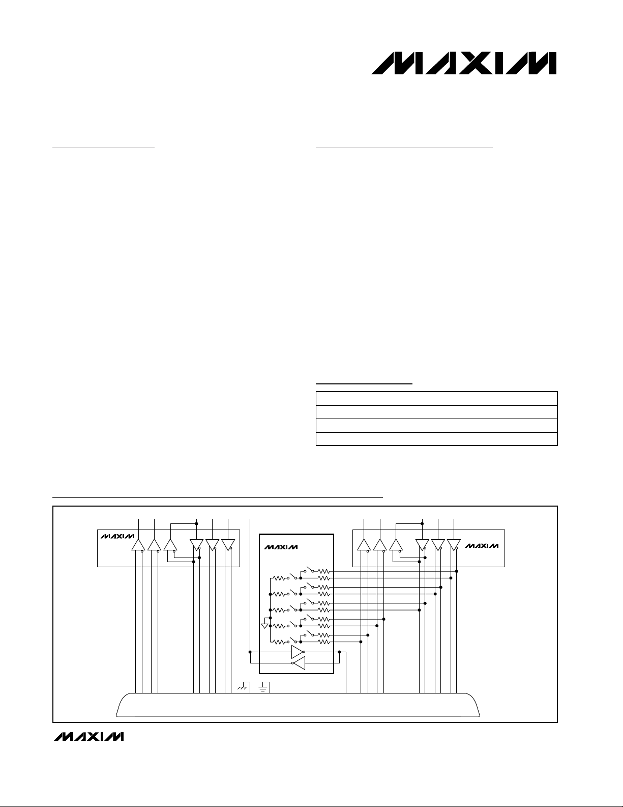
Typical Operating Circuit
Pin Configuration appears at end of data sheet.
For price, delivery, and to place orders, please contact Maxim Distribution at 1-888-629-4642,
or visit Maxim’s website at www.maxim-ic.com.
PART TEMP RANGE PIN-PACKAGE
MAX3172CAI 0°C to +70°C 28 SSOP
MAX3172EAI -40°C to +85°C 28 SSOP
MAX3174CAI 0°C to +70°C 28 SSOP
CTS DSR RTSDTR LLDCD
MAX3171
MAX3173
R2R3
13 5 10 8 22 6 23 20 19 4 1 7 1618 3 9 17 12 15 11 24 14 2
CTS B
CTS A
DSR B
DSR A
D3
R1
DCD B
DCD A
D2
DTR B
DTR A
D1
RTS B
RTS A
SHIELD
MAX3172
MAX3174
SG
DB-25 CONNECTOR
RXD RXC TXDTXC SCTE
D3
R1
R2R3
R4
D4
LL A
RXD B
RXD A
RXC B
RXC A
TXC B
TXC A
SCTE B
SCTE A
D1D2
TXD B
MAX3170
TXD A
Page 2
MAX3172/MAX3174
+3.3V Multiprotocol Software-Selectable
Cable Terminators and Transceivers
2 _______________________________________________________________________________________
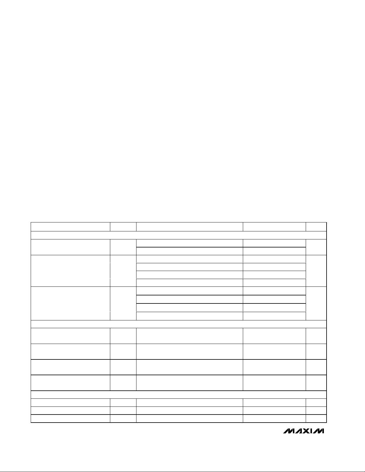
ABSOLUTE MAXIMUM RATINGS
ELECTRICAL CHARACTERISTICS
(VCC= +3.3V ± 5%, TA= T
MIN
to T
MAX
. Typical values are at VCC= +3.3V, TA= +25°C, unless otherwise noted. See Note 2 for V+
and V- input voltage conditions.)
Stresses beyond those listed under “Absolute Maximum Ratings” may cause permanent damage to the device. These are stress ratings only, and functional
operation of the device at these or any other conditions beyond those indicated in the operational sections of the specifications is not implied. Exposure to
absolute maximum rating conditions for extended periods may affect device reliability.
Note 1: V+ and V- can have maximum magnitudes of 7V, but their absolute difference cannot exceed 13V.
(All voltages referenced to GND unless otherwise noted.)
Supply Voltages
V
CC
......................................................................-0.3V to +4V
V+ (Note 1)..........................................................-0.3V to +7V
V- (Note 1) ...........................................................+0.3V to -7V
V+ to V- (Note 1) ...............................................................13V
Logic Input Voltages
M0, M1, M2, DCE/DTE, INVERT, T4IN ................-0.3V to +6V
Logic Output Voltages
R4OUT...................................................-0.3V to (V
CC
+ 0.3V)
Short-Circuit Duration............................................Continuous
Transmitter Outputs
T4OUT ................................................................-15V to +15V
Short-Circuit Duration ........................................................60s
Receiver Input
R4INA .................................................................-15V to +15V
Termination Network Inputs (applied individually)
R_A, R_B ............................................................-15V to +15V
Continuous Power Dissipation (T
A
= +70°C)
28-Pin SSOP (derate 9.52mW/°C above +70°C) ........762mW
Operating Temperature Range
MAX3172CAI/MAX3174CAI...............................0°C to +70°C
MAX3172EAI...................................................-40°C to +85°C
Junction Temperature......................................................+150°C
Storage Temperature Range .............................-65°C to +150°C
Lead Temperature (soldering, 10s) .................................+300°C
DC CHARACTERISTICS
Supply Current
(Digital Inputs = GND or V
V+ Supply Current
(T4IN = GND)
V- Supply Current
(T4IN = V
TERMINATOR NETWORKS (R_A, R_B)
Differential-Mode Impedance
V.35 Mode
Common-Mode Impedance
V.35 Mode
Differential-Mode Impedance
V.11 Mode
Network OFF Impedance I
LOGIC INPUTS (M0, M1, M2, INVERT, DCE/DTE, T4IN)
Input High Voltage V
Input Low Voltage V
Logic Input Current IIH, I
PARAMETER SYMBOL CONDITIONS MIN TYP MAX UNITS
)
CC
CC
I
I
CC
V+
I
V-
Z
IH
IL
)
All modes V.10 receiver inactive 80 200
All modes V.10 receiver active 400 750
No-cable mode
V.10/V.11/V.28/V.35 modes unloaded 0.5 2.5
V.10/V.11 modes T4OUT loaded 11.0 14.0
V.28/V.35 modes T4OUT loaded 3.0 5.0
No-cable mode -0.4 -1.0
V.10/V.11/V.28/V.35 modes unloaded -0.8 -2.5
V.10/V.11 modes T4OUT loaded -11.0 -14.0
V.28/V.35 modes T4OUT loaded -3.0 -5.0
Figure 1, -2V ≤ V
Figure 2, -2V ≤ V
Figure 1, -7V ≤ V
Switches open, -15V ≤ VA ≤ +15V, V
= GND or V
V
B
VIN = VCC or GND ±1 µA
IL
0.2 1.0
≤ +2V 90 104 110 Ω
CM
≤ +2V 135 153 165 Ω
CM
≤ +7V 100 104 110 Ω
CM
= VA,
B
floating
B
50 150 kΩ
2.0 V
0.8 V
µA
mA
mA
Page 3
MAX3172/MAX3174
+3.3V Multiprotocol Software-Selectable
Cable Terminators and Transceivers
_______________________________________________________________________________________ 3
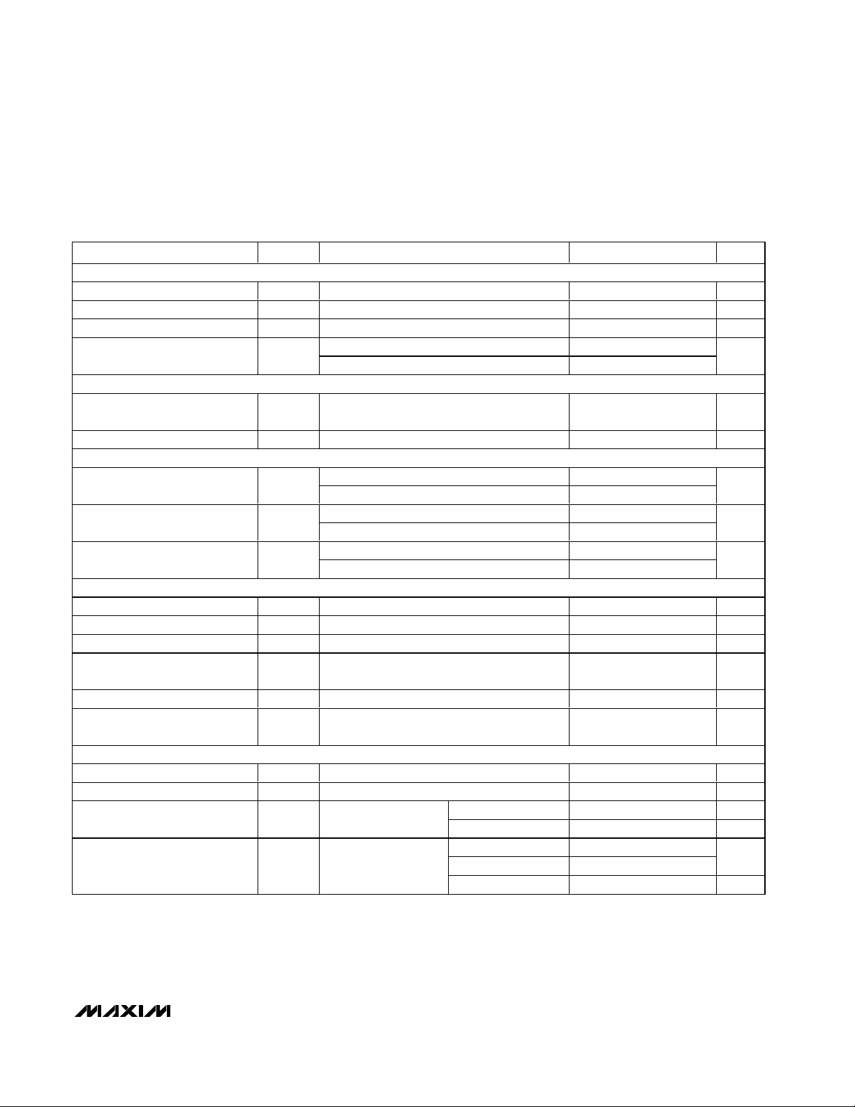
ELECTRICAL CHARACTERISTICS (continued)
(VCC= +3.3V ± 5%, TA= T
MIN
to T
MAX
. Typical values are at VCC= +3.3V, TA= +25°C, unless otherwise noted. See Note 2 for V+
and V- input voltage conditions.)
LOGIC OUTPUT (R4OUT)
Output High Voltage V
Output Low Voltage V
Rise or Fall Time tr, t
Output Leakage Current
(Receiver Output Three-Stated)
TRANSMITTER OUTPUT (T4OUT)
Output Leakage Current I
Data Rate V.10/V.28 240 kbps
RECEIVER INPUT (R4INA)
Receiver Glitch Rejection
(MAX3172 only)
Receiver Input Resistance R
Data Rate
V.10 TRANSMITTER
Output Voltage Swing V
Loaded Output Voltage Swing V
Short-Circuit Current I
Rise or Fall Time tr, t
Transmitter Propagation Delay t
Data Skew
V.10 RECEIVER
Threshold Voltage V
Input Hysteresis ∆V
Receiver Propagation Delay t
Data Skew
PARAMETER SYMBOL CONDITIONS MIN TYP MAX UNITS
PHL
| t
PHL
| t
ODO
PHL
t
PLH
PHL
t
PLH
OH
OL
Z
IN
ODL
SC
, t
TH
TH
, t
I
I
10% to 90%, CL = 15pF 15 ns
f
R4OUT = GND 30 50 100
R4OUT = V
-0.25V < V
power-off or no-cable mode
Minimum pulse width passed 5
Maximum pulse width rejected 15
V.10 enabled, -10V ≤ V
V.28 enabled, -15V ≤ V
MAX3172 64
MAX3174 240
RL = 3.9kΩ, Figure 3 ±4.0 ±4.4 ±6.0 V
RL = 450Ω, Figure 3 0.9 × V
T4OUT = GND ±100 ±150 mA
10% to 90%, RL = 450Ω, CL = 100pF,
f
Figure 3
PLHRL
R
|
Figure 4
PLH
Figure 4
|
= 1.0mA V
SOURCE
= 1.6mA 0.4 V
SINK
CC
< +0.25V,
T4OUT
≤ +10V 20 40
R4INA
≤ +15V 3 5 7
R4INA
= 450Ω, CL = 100pF, Figure 3 2 µs
= 450Ω, CL = 100pF, Figure 3 50 ns
L
MAX3172 5 10 15 µs
MAX3174 60 120 ns
MAX3172CAI 0.5 4
MAX3172EAI 0.5 5
MAX3174 5 16 ns
- 1.0 V
CC
0.1 1
-100 100 µA
ODO
2µs
25 100 250 mV
15 mV
µA
µs
kΩ
kbps
V
µs
Page 4
MAX3172/MAX3174
+3.3V Multiprotocol Software-Selectable
Cable Terminators and Transceivers
4 _______________________________________________________________________________________
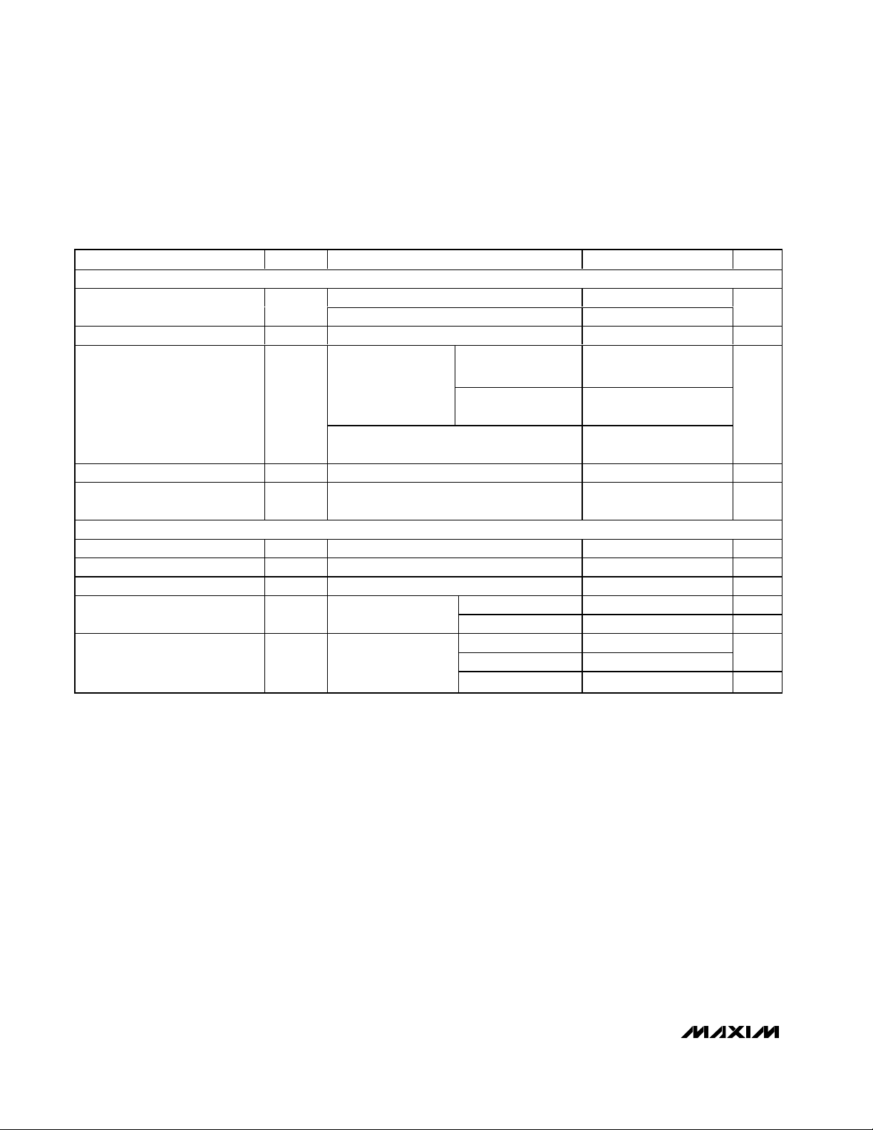
ELECTRICAL CHARACTERISTICS (continued)
(VCC= +3.3V ± 5%, TA= T
MIN
to T
MAX
. Typical values are at VCC= +3.3V, TA= +25°C, unless otherwise noted. See Note 2 for V+
and V- input voltage conditions.)
Note 2: The charge pump on the MAX3171/MAX3173 can supply V+ and V- to the MAX3172/MAX3174. The V+ and V- input levels
vary with the mode of chipset operation as follows:
V.35/V.28 modes: +5.55V ≤ V+ ≤ +6.50V, -6.50V ≤ V- ≤ -5.45V
Typical operation: V+ = +5.90V, V- = -5.80V
V.10/V.11 modes: +4.20V ≤ V+ ≤ +5.0V, -4.60V ≤ V- ≤ -3.80V
Typical operation: V+ = +4.60V, V- = -4.20V
The MAX3171/MAX3173 are guaranteed to provide these V+/V- supply levels.
V.28 TRANSMITTER
Output Voltage Swing V
Short-Circuit Current I
Output Slew Rate SR
Transmitter Propagation Delay t
Data Skew
V.28 RECEIVER
Input Threshold Low V
Input Threshold High V
Input Hysteresis V
Receiver Propagation Delay t
Data Skew
PARAMETER SYMBOL CONDITIONS MIN TYP MAX UNITS
RL = 3kΩ, Figure 3 ±5.0 ±5.4
O
Open circuit, Figure 3 ±6.5
T4OUT = GND ±25 ±60 mA
RL = 3kΩ,
C
= 2500pF
L
measured from +3V
to -3V or -3V to +3V,
Figure 3
R
= 7kΩ , CL = 150pF measured from
L
+3V to -3V or -3V to +3V, Figure 3
PLH
-
|
Figure 4
PLH
Figure 4
|
MAX3172CAI
MAX3174CAI
MAX3172EAI 3 30
MAX3172 5 10 15 µs
MAX3174 200 ns
MAX3172CAI 0.5 4
MAX3172EAI 0.5 5
MAX3174 100 ns
430
630
2.0 1.6 V
PHL
| t
PHL
| t
t
PLH
t
PLH
SC
, t
PHL
IL
IH
HYS
, t
PHL
V
V/µs
1µs
100 ns
1.1 0.8 V
0.5 V
µs
Page 5
MAX3172/MAX3174
+3.3V Multiprotocol Software-Selectable
Cable Terminators and Transceivers
_______________________________________________________________________________________ 5
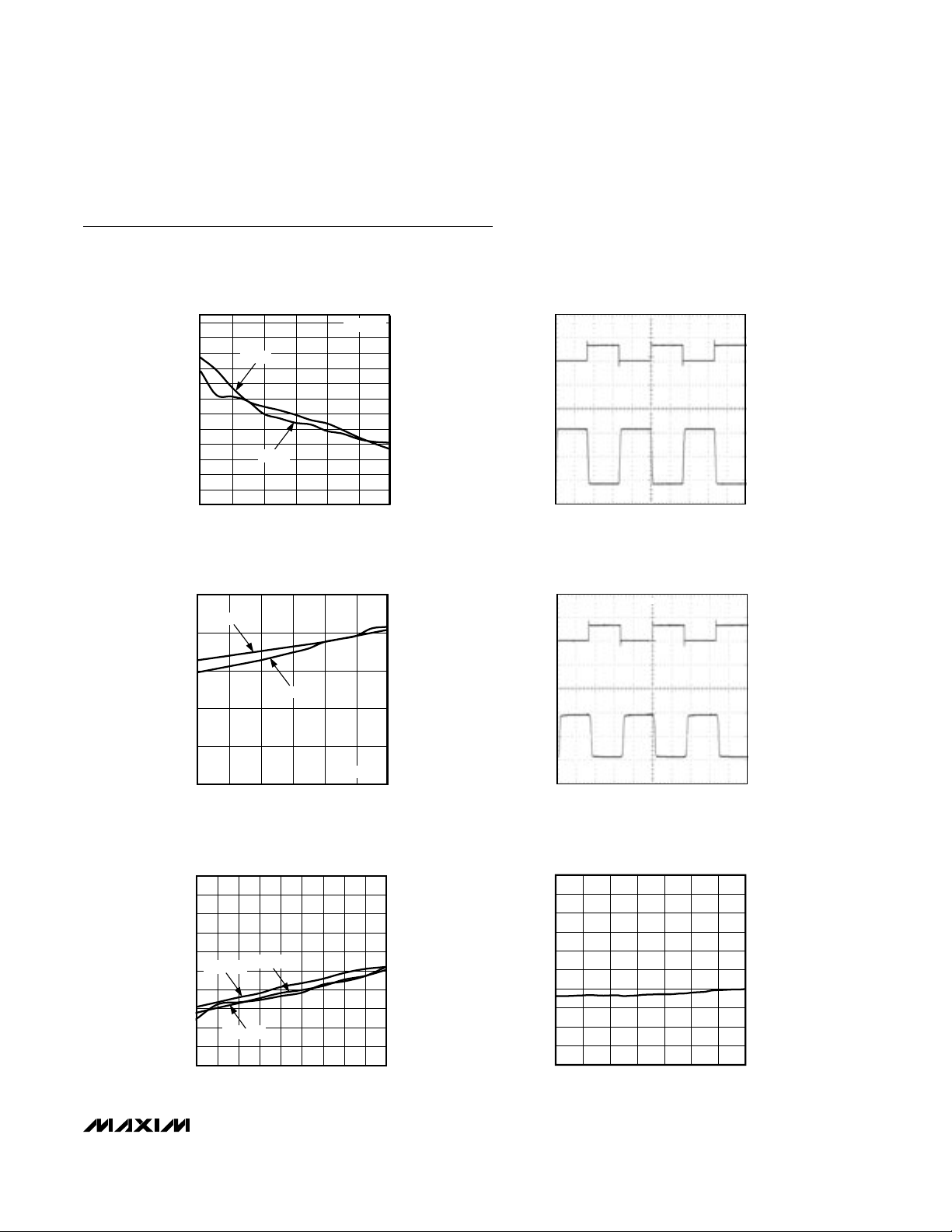
Typical Operating Characteristics
(V
CC
= +3.3V (see Note 2 in Electrical Characteristics table), TA= +25°C, unless otherwise noted.)
V.10 60kbps TRANSMITTER
WAVEFORM (450Ω/100pF)
MAX3172-04
10µs/div
0
5V
0
5V
-5V
5V/div
T4OUT
5V/div
T4IN
100
102
101
104
103
106
105
107
109
108
110
-10 10 20 3004050607080
V.11/V.35 DIFFERENTIAL-MODE
IMPEDANCE vs. TEMPERATURE
MAX3172-05
TEMPERATURE (°C)
DIFFERENTIAL-MODE IMPEDANCE (Ω)
VCM = -7V
VCM = 0
VCM = +7V
100
103
102
101
105
104
109
108
107
106
110
-7 -5 -3 -1 1357
V.11/V.35 DIFFERENTIAL-MODE
IMPEDANCE vs. COMMON-MODE VOLTAGE
MAX3172-06
COMMON-MODE VOLTAGE (V)
DIFFERENTIAL-MODE IMPEDANCE (Ω)
V.28 SLEW RATE
vs. LOAD CAPACITANCE
24
22
20
18
16
14
12
10
SLEW RATE (V/µs)
8
6
4
2
0
+SLEW
-SLEW
500
0
1000 1500
LOAD CAPACITANCE (pF)
2000
RL = 3kΩ
2500
MAX3172-01
3000
V.10 RISE AND FALL TIMES
vs. LOAD CAPACITANCE
2.5
FALL TIME
2.0
1.5
RISE TIME
1.0
MAX3172-03
WAVEFORM (3kΩ/1000pF LOAD)
5V
0
5V
0
-5V
V.28 60kbps TRANSMITTER
10µs/div
MAX3172-02
T4IN
5V/div
T4OUT
5V/div
RISE AND FALL TIMES (µs)
0.5
0
RL = 450Ω
0 1000500 1500 2000 2500 3000
LOAD CAPACITANCE (pF)
Page 6
MAX3172/MAX3174
+3.3V Multiprotocol Software-Selectable
Cable Terminators and Transceivers
6 _______________________________________________________________________________________
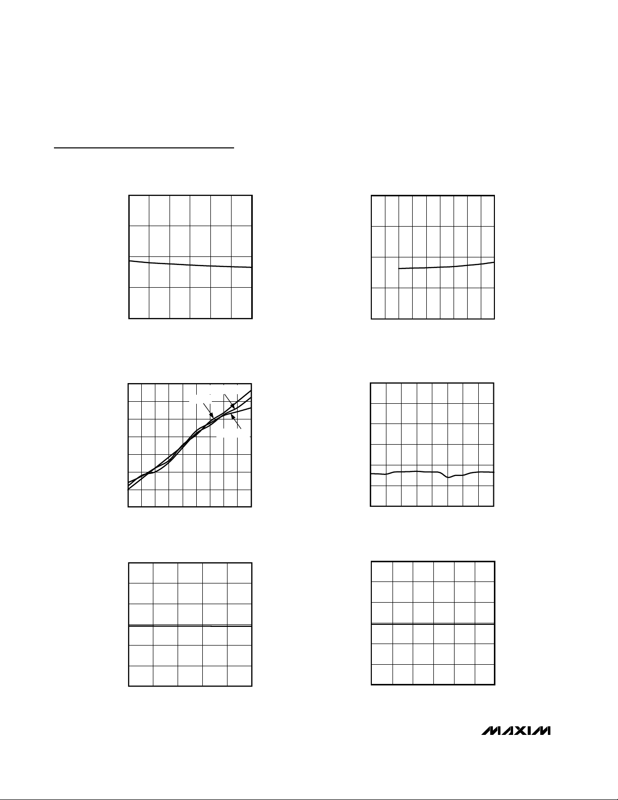
Typical Operating Characteristics (continued)
(V
CC
= +3.3V (see Note 2 in Electrical Characteristics table), TA= +25°C, unless otherwise noted.)
105.0
V.11/V.35 DIFFERENTIAL-MODE
IMPEDANCE vs. V+
V.11/V.35 DIFFERENTIAL-MODE
IMPEDANCE vs. V-
105.0
104.5
104.0
103.5
DIFFERENTIAL-MODE IMPEDANCE (Ω)
103.0
4.2 4.84.4 4.6 5.0 5.2 5.4
V+ (V)
V.35 COMMON-MODE IMPEDANCE
154
153
152
151
150
149
COMMON-MODE IMPEDANCE (Ω)
148
147
-10 10 200304050607080
vs. TEMPERATURE
VCM = 2.0V
VCM = 0
VCM = -2.0V
TEMPERATURE (°C)
MAX3172-07
MAX3172-09
104.5
104.0
103.5
DIFFERENTIAL-MODE IMPEDANCE (Ω)
103.0
-5.4 -4.4-4.6-5.0-5.2 -4.8 -4.2 -4.0 -3.8 -3.6
V- (V)
V.35 COMMON-MODE IMPEDANCE
vs. COMMON-MODE VOLTAGE
154
153
152
151
150
COMMON-MODE IMPEDANCE (Ω)
149
148
-2.0 -1.0-1.5 -0.5 0 0.5 1.0 1.5 2.0
COMMON-MODE VOLTAGE (V)
MAX3172-08
MAX3172-10
V.35 COMMON-MODE
IMPEDANCE vs. V+
165
160
155
150
145
COMMON-MODE IMPEDANCE (Ω)
140
135
5.5 5.95.7 6.1 6.3 6.5
V+ (V)
MAX3172-11
165
160
155
150
145
COMMON-MODE IMPEDANCE (Ω)
140
135
-6.6 -6.2 -6.0-6.4 -5.8 -5.6 -5.4
V.35 COMMON-MODE
IMPEDANCE vs. V-
V- (V)
MAX3172-12
Page 7

MAX3172/MAX3174
+3.3V Multiprotocol Software-Selectable
Cable Terminators and Transceivers
_______________________________________________________________________________________ 7
Figure 1. V.11 or V.35 Differential Impedance Measurement
Figure 2. V.35 Common-Mode Impedance Measurement
Figure 3. V.10/V.28 Driver Test Circuit
Figure 4. V.10/V.28 Receiver Test Circuit
Test Circuits
A
R1
52Ω
OHMMETER
B
S1 ON
R3
127Ω
S2 OFF
R2
52Ω
VCM = ±7V OR ±2V
A
R1
52Ω
S1 ON
R3
OHMMETER
R2
VCM = ±2V
B
52Ω
127Ω
S2 ON
T
C
L
TR
R
L
15pF
Page 8

MAX3172/MAX3174
+3.3V Multiprotocol Software-Selectable
Cable Terminators and Transceivers
8 _______________________________________________________________________________________
Pin Description
PIN NAME FUNCTION
1M2Mode-Select Pin (see Tables 1 and 3 for detailed information)
2M1Mode-Select Pin (see Tables 1 and 3 for detailed information)
3M0Mode-Select Pin (see Tables 1 and 3 for detailed information)
4V
5 R5A Termination Network 5 Node A
6 R5B Termination Network 5 Node B
7 T4IN Transmitter CMOS Input
8 R4OUT Receiver CMOS Output
9,18, 22 GND Ground
10 R4B Termination Network 4 Node B
11 R4A Termination Network 4 Node A
12 R3C Termination Network 3 Node C
13 R3B Termination Network 3 Node B
14 R3A Termination Network 3 Node A
15 R1A Termination Network 1 Node A
16 R1B Termination Network 1 Node B
CC
+3.3V Supply Voltage (±5%). Bypass VCC to GND with a 0.1µF capacitor.
17 R1C Termination Network 1 Node C
19 R2C Termination Network 2 Node C
20 R2B Termination Network 2 Node B
21 R2A Termination Network 2 Node A
23 R4INA Inverting Receiver Input
24 V-
25 T4OUT Inverting Transmitter Output
26 V+
27 DCE/DTE
28 INVERT
Negative Supply (connect to V- pin of MAX3171/MAX3173). Bypass V- to GND with
a 0.1µF capacitor.
Positive Supply (connect to V+ pin of MAX3171/MAX3173). Bypass V+ to GND with
a 0.1µF capacitor.
DCE/DTE Mode-Select Pin. Logic level LOW selects DTE interface. See Tables 1
and 3 for detailed information.
Mode-Select Pin (inverts functionality of DCE/DTE input for T4/R4). See Tables 1 and
3 for detailed information.
Page 9

MAX3172/MAX3174
+3.3V Multiprotocol Software-Selectable
Cable Terminators and Transceivers
_______________________________________________________________________________________ 9
Detailed Description
The MAX3172/MAX3174 contain five software-selectable
multiprotocol cable termination networks. Each network is
capable of terminating V.11 transceivers (RS-422, RS530, RS-530A, RS-449, V.36, and X.21) with a 100Ω differential load, V.35 transceivers with a T-network load, or
V.28 (RS-232) and V.10 transceivers (RS-423) with an
open circuit load. The MAX3172/MAX3174, along with the
MAX3170 and MAX3171/MAX3173, form a complete
+3.3V software-selectable DTE or DCE interface port supporting V.11/RS-422, RS-530, RS-530A, V.36/RS-449,
V.35, V.28/RS-232, V.10/RS-423, and X.21 serial interfaces.
The MAX3172/MAX3174 also contain a multiprotocol
transceiver that is software-selectable between V.10 and
V.28 operation modes. This transceiver is intended as the
handshake signal I/O in a DCE/DTE port application, and
is designed to use V+ and V- levels generated by the
MAX3171/MAX3173 charge pump. The MAX3172 features 10µs deglitching on the V.10/V.28 receiver input to
allow unterminated operation. The MAX3174 is used in
applications that do not require deglitching on the serial
handshake signals.
No-Cable Mode
The MAX3172/MAX3174 enter no-cable mode when the
mode-select inputs are all HIGH (M0 = M1 = M2 = 1). In
this mode, the driver, receiver, and bias circuitry are disabled, and the supply current drops to less than 200µA.
In no-cable mode, all five termination networks are
placed in the V.11 mode of operation (shorting pins R_A
and R_B with a 100Ω resistor). The receiver output enters
a high-impedance state in no-cable mode, allowing this
output line to be shared with other receivers (the receiver
output has an internal pullup resistor to pull the output
HIGH if not driven). Also, in no-cable mode, the transmitter output enters a high-impedance state so that this output can be shared with other devices.
Cable Termination
The MAX3172/MAX3174 software-selectable resistor networks are intended for use with the MAX3170 clock/data
transceiver chip. The termination network is used for the
V.11, V.35, and V.28 transmitters. The MAX3172/
MAX3174 provide the advantage of not having to build
expensive termination networks from resistors and relays,
manually changing termination modules, or building termination networks into custom cables.
Each termination network can be in one of three modes:
V.35, V.11, or high impedance (high-Z) as shown in
Figure 5 (see Table 2). For example, in V.35 mode, all five
Table 1. Termination Mode Selection
Table 2. Switch Configuration by Mode
MODE M2 M1 M0 DCE/DTE INVERT R1 R2 R3 R4 R5
V.10/RS-423 0 0 0 0 X Z Z Z Z Z
RS-530A 0 0 1 0 X Z Z V.11 V.11 V.11
RS-530 0 1 0 0 X Z Z V.11 V.11 V.11
X.21 0 1 1 0 X Z Z V.11 V.11 V.11
V.35 1 0 0 0 X V.35 V.35 V.35 V.35 V.35
RS-449/V.36 1 0 1 0 X Z Z V.11 V.11 V.11
V.28/RS-232 1 1 0 0 X Z Z Z Z Z
No Cable 1 1 1 0 X V.11 V.11 V.11 V.11 V.11
V.10/RS-423 0 0 0 1 X Z Z Z Z Z
RS-530A 0 0 1 1 X Z Z Z V.11 V.11
RS-530 0 1 0 1 X Z Z Z V.11 V.11
X.21 0 1 1 1 X Z Z Z V.11 V.11
V.35 1 0 0 1 X V.35 V.35 V.35 V.35 V.35
RS-449/V.36 1 0 1 1 X Z Z Z V.11 V.11
V.28/RS-232 1 1 0 1 X Z Z Z Z Z
No Cable 1 1 1 1 X V.11 V.11 V.11 V.11 V.11
MODE SW1 SW2
V.35 ON ON
V.11 ON OFF
V.28/V.10 (Z) OFF OFF
Page 10

MAX3172/MAX3174
+3.3V Multiprotocol Software-Selectable
Cable Terminators and Transceivers
10 ______________________________________________________________________________________
networks are configured to provide 100Ω differential
impedance and 150Ω common-mode impedance to terminate the MAX3170 V.35 transmitter outputs and receiver inputs.
Termination Mode Selection
The mode-select pins M0, M1, M2, and DCE/DTE control
the state of the five termination networks (Table 1). The
mode-select table of the MAX3172/MAX3174 is compatible with the MAX3170 mode-select table so that the M0,
M1, M2, and DCE/DTE pins can be connected to the corresponding pins on the MAX3170. For example, M2 = 1,
M1 = 0, M0 = 0 corresponds to V.35 mode for both the
MAX3172/MAX3174 and the MAX3170 clock/data transceiver chip.
R4/T4 Mode Selection
The MAX3172/MAX3174 include a transceiver for use in
applications requiring an extra serial handshake signal
(for example, local loopback). The transceiver can be
Table 3. R4/T4 Mode-Select Table
Not Used (Default V.11) 0 0 0 0 0 Z V.10
RS-530A 0 0 1 0 0 Z V.10
RS-530 0 1 0 0 0 Z V.10
X.21 0 1 1 0 0 Z V.10
V.35 1 0 0 0 0 Z V.28
RS-449/V.36 1 0 1 0 0 Z V.10
V.28/RS-232 1 1 0 0 0 Z V.28
No Cable 1 1 1 0 0 Z Z
Not Used (Default V.11) 0 0 0 1 0 V.10 Z
RS-530A 0 0 1 1 0 V.10 Z
RS-530 0 1 0 1 0 V.10 Z
X.21 0 1 1 1 0 V.10 Z
V.35 1 0 0 1 0 V.28 Z
RS-449/V.36 1 0 1 1 0 V.10 Z
V.28/RS-232 1 1 0 1 0 V.28 Z
No Cable 1 1 1 1 0 Z Z
Not Used (Default V.11) 0 0 0 0 1 V.10 Z
RS-530A 0 0 1 0 1 V.10 Z
RS-530 0 1 0 0 1 V.10 Z
X.21 0 1 1 0 1 V.10 Z
V.35 1 0 0 0 1 V.28 Z
RS-449/V.36 1 0 1 0 1 V.10 Z
V.28/RS-232 1 1 0 0 1 V.28 Z
No Cable 1 1 1 0 1 Z Z
Not Used (Default V.11) 0 0 0 1 1 Z V.10
RS-530A 0 0 1 1 1 Z V.10
RS-530 0 1 0 1 1 Z V.10
X.21 0 1 1 1 1 Z V.10
V.35 1 0 0 1 1 Z V.28
RS-449/V.36 1 0 1 1 1 Z V.10
V.28/RS-232 1 1 0 1 1 Z V.28
No Cable 1 1 1 1 1 Z Z
PROTOCOL M2 M1 M0 DCE/DTE INVERT T4 R4
Page 11

MAX3172/MAX3174
+3.3V Multiprotocol Software-Selectable
Cable Terminators and Transceivers
______________________________________________________________________________________ 11
configured for V.10 or V.28 operation as a driver or
receiver (Table 3). This mode-selection table is compatible for use with the MAX3170 (clock/data transceiver)
and the MAX3171/MAX3173 (control transceiver). For
example, if X.21 mode is selected in DCE mode (M2 = 0,
M1 = 1, M0 = 1, and DCE/DTE = 1), the MAX3170,
MAX3171/MAX3173, and MAX3172/MAX3174 transceivers will all be placed in X.21 DCE mode.
Fail-Safe
The MAX3172/MAX3174 guarantee a logic HIGH
receiver output when the receiver input is shorted to
GND or when it is connected to a terminated transmission line with the driver disabled. The V.10 receiver
threshold is between +25mV and +250mV. If the V.10
receiver input voltage is less than +25mV, R4OUT is
logic HIGH. If the V.10 receiver input is greater than
+250mV, R4OUT is logic LOW.
The V.28 receiver threshold is between +0.8V and
+2.0V. If the V.28 receiver input voltage is less than
+0.8V, R4OUT is logic HIGH. If the receiver input is
greater than +2.0V, R4OUT is logic LOW. If the driving
transmitter is disabled or disconnected, the receiver’s
input voltage is pulled to zero by its internal termination.
With the receiver thresholds of the MAX3172/MAX3174,
this results in a logic HIGH.
Applications Information
Older multiprotocol cable termination implementations
have been constructed using expensive relays with discrete resistors, custom cables with built-in termination,
or complex circuit board configurations to route signals
to the correct termination. The MAX3172/MAX3174 provide a simple solution to this termination problem. All
required termination configurations are software selectable using four mode-control input pins (M2, M1, M0,
and DCE/DTE).
V.11 Termination
For high-speed data transmission, the V.11 specification recommends terminating the cable at the receiver
Figure 6. Typical V.11 Interface
A
B
S2 OFF
V.11 MODE V.35 MODE HIGH-Z MODE
A
C*
B
S2 ON
S1 OFF
A
B
S2 OFF
C*
C*
*NODE C IS PROVIDED IN NETWORKS 1,2,3.
R2
52Ω
R1
52Ω
S1 ON
R3
127Ω
R2
52Ω
R1
52Ω
S1 ON
R3
127Ω
R2
52Ω
R1
52Ω
R3
127Ω
Figure 5. MAX3172/MAX3174 Termination Network Configurations
BALANCED
INTERCONNECTING
GENERATOR
CABLE
TERMINATION
A
B
C
A′
B′
C′
CABLE
100Ω
MIN
LOAD
RECEIVER
Page 12

MAX3172/MAX3174
+3.3V Multiprotocol Software-Selectable
Cable Terminators and Transceivers
12 ______________________________________________________________________________________
with a minimum of a 100Ω resistor (Figure 6). This resistor, although not required, prevents reflections from
corrupting transmitted data.
In Figure 7, the MAX3172/MAX3174 are used to termi-
nate the V.11 receiver. Internal to the MAX3172/
MAX3174, S1 is closed and S2 is open to present a
104Ω typical differential resistance and high-Z common-mode impedance. S3 opens to disable the
MAX3170’s internal V.28 termination.
The V.11 specification allows for signals with commonmode variations of ±7V with differential signal amplitudes from 2V to 6V. Also, data rates may be as high as
10Mbps. The MAX3172/MAX3174 maintain steady termination impedance between 100Ω and 110Ω over
these conditions.
V.35 Termination
Figure 8 shows a standard V.35 interface. The genera-
tor and the load must both present a 100Ω ±1 0 Ω differ-
ential impedance and a 150Ω ±1 5 Ω common-mode
impedance (as shown by the resistive T-networks in
Figure 8). The V.35 driver generates a current output
(typically ±11mA) that develops an output voltage
between 440mV and 660mV across the load termination networks.
Figure 8. Typical V.35 Interface
Figure 7. V.11 Termination and Internal Resistance Networks
A′
R1
52Ω
S1
R2
52Ω
B′
C′
MAX3172
MAX3174
R3
127Ω
S2
GENERATOR
A
A
B
BALANCED
INTERCONNECTING
CABLE
GND
R5
30kΩ
R8
5kΩ
S3
30kΩ
A′
R6
10kΩ
R7
10kΩ
R4
CABLE
TERMINATION
MAX3170
RECEIVER
LOAD
RECEIVER
50Ω
125Ω
50Ω
B
C
B′
C′
125Ω
50Ω
50Ω
Page 13

MAX3172/MAX3174
+3.3V Multiprotocol Software-Selectable
Cable Terminators and Transceivers
______________________________________________________________________________________ 13
In Figure 9, the MAX3172/MAX3174 are used to imple-
ment the resistive T-network that is needed to properly
terminate the V.35 driver and receiver. Internal to the
MAX3172/MAX3174, S1 and S2 are closed to connect
the T-network resistors to the circuit. The V.28 termina-
tion resistor, internal to the MAX3170, is disabled by
opening S3 to avoid interference with the T-network
impedance.
The V.35 specification allows for ±4V of ground difference between the V.35 generator and V.35 load. The
V.35 data rates may be as high as 10Mbps. The
MAX3172/MAX3174 maintain correct terminal impedances over these conditions.
V.35 EMI Reduction
For applications where EMI reduction is especially
important, the MAX3172/MAX3174 termination networks provide a pin for shunting common-mode driver
currents to GND (Figure 10). Mismatches between A
and B driver output propagation delays create a common-mode disturbance on the cable. This commonmode energy can be shunted to GND by placing a
100pF capacitor (C1 to GND) from the center point of
the T-network termination (R1C, R2C, and R3C).
V.28 Termination
Most industry-standard V.28 receivers (including the
MAX3170) do not require external termination because
the receiver includes an internal 5kΩ termination resistor. When the MAX3172/MAX3174 are placed in V.28
mode, all five of the termination networks are placed in
a high-Z mode. In high-Z mode, the MAX3172/
MAX3174 termination networks will not interfere with the
MAX3170's internal 5kΩ termination.
Figure 9. V.35 Termination and Internal Resistance Networks
Figure 10. V.35 Driver
R3
127Ω
R2
52Ω
R1
52Ω
A
B
C(GND)
MAX3172
MAX3174
S1
S2
C1
100pF
DRIVER
R_C
A′
R1
52Ω
S1
R2
52Ω
B′
C′
MAX3172
MAX3174
R3
127Ω
S2
A
R5
30kΩ
R8
5kΩ
S3
B
GND
R4
30kΩ
10kΩ
10kΩ
R6
R7
MAX3170
RECEIVER
Page 14

MAX3172/MAX3174
+3.3V Multiprotocol Software-Selectable
Cable Terminators and Transceivers
14 ______________________________________________________________________________________
In Figure 11, the MAX3170 and MAX3172/MAX3174 are
placed in V.28 mode. Switches S1 and S2 are opened
on the MAX3172/MAX3174 to place the network in highZ mode. Switch S3 is closed on the MAX3170 to enable
the 5kΩ terminating resistor.
V.28 Interface
The V.28 interface is an unbalanced single-ended interface (Figure 12). The V.28 driver generates a minimum
of ±5V across the load impedance between A' and C'.
The V.28 receiver specification calls for input trip points
at ±3V. To aid in rejecting system noise, the MAX3170
V.28 receiver has a typical hysteresis of 0.5V. Also, the
MAX3172/MAX3174 have more tightly specified input
trip points to guarantee fail-safe operation (see Fail-
Safe).
The MAX3172/MAX3174 V.28 receiver provides an
internal 5kΩ termination resistance.
V.10 Interface
The V.10 interface (Figure 12) is an unbalanced singleended interface capable of driving a 450Ω load. The
V.10 driver generates a minimum voltage of ±4V
(V
ODO
) across A' and C' when unloaded and a mini-
mum voltage of ±0.9 ✕V
ODO
when loaded with 450Ω.
The V.10 receiver input trip threshold is defined
between +300mV and -300mV with input impedance
characteristics shown in Figure 13.
The MAX3172/MAX3174 V.10 mode receiver has a
threshold between +25mV and +250mV to ensure that
the receiver has proper fail-safe operation (see Fail-
Safe). To aid in rejecting system noise, the MAX3172/
MAX3174 V.10 receiver has a typical hysteresis of
15mV. Switch S3 in Figure 14 is open in V.10 mode to
disable the 5kΩ V.28 termination at the receiver input.
Receiver Glitch Rejection
To allow operation in an unterminated or otherwise
noisy system, the MAX3172 features 10µs of receiver
input glitch rejection. The glitch-rejection circuitry
blocks the reception of high-frequency noise with a bit
period less than 5µs while receiving low-frequency signals with a bit period greater than 15µs, allowing glitchfree operation in unterminated systems at up to 64kbps.
Figure 12. Typical V.28 and V.10 Interface
Figure 11. V.28 Termination and Internal Resistance Networks
Figure 13. V.10 Receiver Input Impedance
A′
R1
MAX3172
52Ω
MAX3174
S1
R2
52Ω
B′
C′
GENERATOR
-10V
-3.25mA
UNBALANCED
INTERCONNECTING
CABLE
A
C
I
Z
-3V
TERMINATION
A′
C′
S2
+3V
CABLE
R3
127Ω
LOAD
RECEIVER
3.25mA
+10V
A
R5
30kΩ
R8
5kΩ
S3
B
GND
R4
30kΩ
10kΩ
10kΩ
R6
R7
MAX3170
RECEIVER
V
Z
Page 15

MAX3172/MAX3174
+3.3V Multiprotocol Software-Selectable
Cable Terminators and Transceivers
______________________________________________________________________________________ 15
The MAX3174 does not have this glitch rejection and
can be operated at frequencies up to 240kbps if properly terminated.
DCE vs. DTE Operation
Figure 15 illustrates a DCE or DTE controller-selectable
interface. The DCE/DTE input switches the MAX3172/
MAX3174s’ mode of operation. Logic high selects DCE,
which enables driver 4 on the MAX3172/MAX3174
(INVERT = 0), driver 3 on the MAX3171/MAX3173, and
driver 3 on the MAX3170. A logic low selects DTE,
which enables receiver 4 on the MAX3172/MAX3174
(INVERT = 0), receiver 1 on the MAX3171/MAX3173,
and receiver 1 on the MAX3170.
This application requires only one DB-25 connector.
See Figure 15 for complete signal routing in DCE and
DTE modes. For example, driver 4 routes the LL(DCE)
signal to pin 18 in DCE mode, while in DTE mode,
receiver 4 routes pin 18 to the LL(DTE) signal.
Complete Multiprotocol X.21 Interface
A complete DTE-to-DCE interface operating in X.21
mode is shown in Figure 16. The MAX3172/MAX3174 terminate the V.11 clock and data signals, and its transceiver carries the local loopback (LL) signal. The MAX3170
carries the clock and data signals, and the
MAX3171/MAX3173 carry the control signals. The control
signals generally do not require external termination.
Compliance Testing
A European Standard EN45001 test report is available
for the MAX3170–MAX3174 chipset. A copy of the test
report is available from Maxim upon request.
R6
10kΩ
R8
5kΩ
A′
C′
A
GND
R5
30kΩ
R7
10kΩ
R4
30kΩ
MAX3172
MAX3174
S3
RECEIVER
Figure 14. V.10 Internal Resistance Networks
Page 16

MAX3172/MAX3174
+3.3V Multiprotocol Software-Selectable
Cable Terminators and Transceivers
16 ______________________________________________________________________________________
Figure 15. Multiprotocol DCE/DTE Port
MAX3171
MAX3173
CTS(DTE)
RTS(DCE)
DSR(DTE)
DTR(DCE)
R2R3
R1
DCD(DTE)
DCD(DCE)
D3
DTR(DTE)
DSR(DCE)
D2
RTS(DTE)
CTS(DCE)
D1
13 5 10 8 22 6 23 20 19 4 1 7 18 16 3 9 17 12 15 11 24 14 2
DTE
CTS B
CTS A
DSR B
DSR A
DCE
RTS B
RTS A
DTR B
DTR A
DCD B
DCD B
DCD A
DCD A
DTR B
DSR B
DTR A
DSR A
RTS B
CTS B
RTS A
CTS A
M1M2M0
DCE/DTE
SHIELD
RXD(DTE)
TXD(DCE)
LL(DTE)
LL(DCE)
MAX3172
MAX3174
R4
D4
DCE/DTE
M2M1M0
SG
LL A
DB-25 CONNECTOR
LL A
RXC(DTE)
SCTE(DCE)
RXD B
RXD A
TXD B
TXD A
R2R3
RXC B
SCTE B
R1
RXC A
SCTE A
TXC(DTE)
TXC(DCE)
D3
TXC B
TXC B
SCTE(DTE)
RXC(DCE)
TXC A
SCTE B
TXC A
RXC B
TXD(DTE)
RXD(DCE)
D1D2
TXD B
SCTE A
RXC A
RXD B
TXD A
RXD A
MAX3170
M1M2M0
M1M2M0
DCE/DTE
DCE/DTE
Page 17

MAX3172/MAX3174
+3.3V Multiprotocol Software-Selectable
Cable Terminators and Transceivers
______________________________________________________________________________________ 17
Figure 16. DCE-TO-DTE X.21 Interface
SERIAL
CONTROLLER
SCTE
TXD
TXC
RXC
RXD
RTS
DTE
MAX3170
D1
D2
D3
R1
R2
R3
LL
MAX3171
MAX3173
D1
MAX3172
MAX3174
103Ω
103Ω
103Ω
D4
R4
TXD
SCTE
TXC
RXC
RXD
LL
RTS
MAX3174
103Ω
103Ω
R4
D4
DCE
MAX3170MAX3172
MAX3171
MAX3173
SERIAL
CONTROLLER
R3
R2
R1
D3
D2
D1
R3
TXD
SCTE
TXC
RXC
RXD
LL
RTS
DTR
DCD
DSR
CTS
D2
D3
R1
R2
R3
DTR
DCD
DSR
CTS
R2
R1
D3
D2
D1
DTR
DCD
DSR
CTS
Page 18

MAX3172/MAX3174
+3.3V Multiprotocol Software-Selectable
Cable Terminators and Transceivers
18 ______________________________________________________________________________________
Pin Configuration
28
27
26
25
24
23
22
21
20
19
18
17
16
15
1
2
3
4
5
6
7
8
9
10
11
12
13
14
INVERT
DCE/DTE
V+
T4OUT
V-
R4INA
R1A
GND
R2A
R2B
R2C
GND
R1C
R1B
R3A
R3B
R3C
R4A
R4B
GND
R4OUT
T4IN
R5B
R5A
V
CC
M0
M1
M2
28 SSOP
TOP VIEW
MAX3172
MAX3174
Chip Information
TRANSISTOR COUNT: 2506
Page 19

+3.3V Multiprotocol Software-Selectable
Cable Terminators and Transceivers
Maxim cannot assume responsibility for use of any circuitry other than circuitry entirely embodied in a Maxim product. No circuit patent licenses are
implied. Maxim reserves the right to change the circuitry and specifications without notice at any time.
Maxim Integrated Products, 120 San Gabriel Drive, Sunnyvale, CA 94086 408-737-7600 ____________________ 19
© 2004 Maxim Integrated Products Printed USA is a registered trademark of Maxim Integrated Products.
MAX3172/MAX3174
Package Information
(The package drawing(s) in this data sheet may not reflect the most current specifications. For the latest package outline information,
go to www.maxim-ic.com/packages
.)
e
D
12
INCHES
DIM
MIN
A
0.068
A1
0.002
B
0.010
C
HE
N
A
B
A1
D
E
e
H
L
0.004
SEE VARIATIONS
0.205
0.0256 BSC
0.301
0.025
0∞
L
MAX
0.078
0.008
0.015
0.008
0.212
0.311
0.037
8∞
MILLIMETERS
MAX
MIN
1.73 1.99
0.21
0.05
0.38
0.25
0.20
0.09
5.38
5.20
0.65 BSC
7.90
7.65
0.63
0.95
0∞
8∞
INCHES
MIN
D
0.239
D
0.239
D
0.278
D
0.317
0.397
D
MAX
0.249
0.249
0.289
0.328
0.407
MILLIMETERS
MAX
MIN
6.07
6.33
6.07
6.33
7.07
7.33
8.07
8.33
10.07
10.33
N
14L
16L
20L
24L
28L
C
SSOP.EPS
NOTES:
1. D&E DO NOT INCLUDE MOLD FLASH.
2. MOLD FLASH OR PROTRUSIONS NOT TO EXCEED .15 MM (.006").
3. CONTROLLING DIMENSION: MILLIMETERS.
4. MEETS JEDEC MO150.
5. LEADS TO BE COPLANAR WITHIN 0.10 MM.
PROPRIETARY INFORMATION
TITLE:
PACKAGE OUTLINE, SSOP, 5.3 MM
21-0056
REV.DOCUMENT CONTROL NO.APPROVAL
1
C
1
 Loading...