

Page 1
General Description
The MAX3171/MAX3173 are three-driver/three-receiver
multiprotocol transceivers that operate from a single
+3.3V supply. The MAX3171/MAX3173, along with the
MAX3170 and MAX3172/MAX3174, form a complete
software-selectable data terminal equipment (DTE) or
data communications equipment (DCE) interface port
that supports V.28 (RS-232) and V.10/V.11 (RS-449,
V.36, EIA-530, EIA-530-A, X.21, RS-423) protocols. The
MAX3171/MAX3173 transceivers carry the serial interface control signaling; the MAX3170 transceivers carry
the clock and data signals. The MAX3172/
MAX3174 have an extra transceiver for applications
requiring four transceivers for control signaling.
An internal charge pump and proprietary low-dropout
transmitter output stage allow V.28, V.11, and V.10
compliant operation from a single +3.3V supply. A nocable mode is entered when all mode pins (M0, M1,
and M2) are pulled high or left unconnected. In nocable mode, supply current decreases to 2mA and all
transmitter and receiver outputs are disabled (high
impedance). Short-circuit limiting and thermal-shutdown circuits protect the drivers against excessive
power dissipation.
The MAX3171 features 10µs deglitching on the
V.10/V.11/V.28 receiver inputs. The MAX3173 is available for applications that do not require deglitching on
the serial handshake signals.
These parts require only four surface-mount capacitors
for charge-pump operation in addition to supply
bypassing.
Features
♦ Industry’s First +3.3V Multiprotocol Transceiver
♦ Certified TBR-1 and TBR-2 Compliant
(NET1 and NET2)
♦ Supports V.28 (RS-232) and V.10/V.11 (RS-449,
V.36, EIA-530, EIA-530-A, X.21, RS-423) Protocols
♦ 3V/5V Logic Compatibility
♦ Software-Selectable DCE/DTE
♦ True Fail-Safe Receiver Operation
♦ Available in Small 28-Pin SSOP Package
♦ 10µs Receiver Input Deglitching (MAX3171 only)
♦ All Transmitter Outputs Fault Protected to ±15V,
Tolerate Cable Miswiring
________________________Applications
Data Networking PCI Cards
CSU and DSU Telecommunications
Data Routers
MAX3171/MAX3173
+3.3V Multiprotocol 3Tx/3Rx
Software-Selectable Control Transceivers
________________________________________________________________ Maxim Integrated Products 1
19-1703; Rev 1; 8/01
Ordering Information
Typical Operating Circuit
Pin Configuration appears at end of data sheet
For pricing, delivery, and ordering information, please contact Maxim/Dallas Direct! at
1-888-629-4642, or visit Maxim’s website at www.maxim-ic.com.
CTS DSR RTSDTR LLDCD
PART TEMP. RANGE PIN-PACKAGE
MAX3171CAI 0°C to +70°C 28 SSOP
MAX3173CAI 0°C to +70°C 28 SSOP
RXD RXC TXDTXC SCTE
MAX3171
MAX3173
R2R3
13 5 10 8 22 6 23 20 19 4 1 7 1618 3 9 17 12 15 11 24 14 2
CTS B
CTS A
DSR B
DSR A
D3
R1
DCD B
DCD A
D2
DTR B
DTR A
D1
RTS B
RTS A
SHIELD
MAX3172
MAX3174
R4
SG
DB-25 CONNECTOR
R2R3
D4
LL A
RXD A
RXD B
RXC B
RXC A
D3
R1
TXC B
TXC A
SCTE B
SCTE A
D1D2
TXD B
MAX3170
TXD A
Page 2
MAX3171/MAX3173
+3.3V Multiprotocol 3Tx/3Rx
Software-Selectable Control Transceivers
2 _______________________________________________________________________________________
ABSOLUTE MAXIMUM RATINGS
ELECTRICAL CHARACTERISTICS
(VCC= 3.3V ±5%; C1 = C2 = 1µF, C3 = C4 = C5 = 3.3µF, and TA= T
MIN
to T
MAX
, unless otherwise noted. Typical values are at V
CC
= +3.3V, TA= +25°C.) (Note 2)
Stresses beyond those listed under “Absolute Maximum Ratings” may cause permanent damage to the device. These are stress ratings only, and functional
operation of the device at these or any other conditions beyond those indicated in the operational sections of the specifications is not implied. Exposure to
absolute maximum rating conditions for extended periods may affect device reliability.
Note 1: V+ and V- can have maximum magnitudes of 7V, but their absolute difference cannot exceed 13V.
(All voltages referenced to GND unless otherwise noted.)
Supply Voltages
V
CC
......................................................................-0.3V to +4V
V+ (Note 1) ..........................................................-0.3V to +7V
V- (Note 1) ...........................................................+0.3V to -7V
V+ to V- (Note 1) ...............................................................13V
Logic Input Voltages
M0, M1, M2, DCE/DTE, T_IN ...............................-0.3V to +6V
Logic Output Voltages
R_OUT...................................................-0.3V to (V
CC
+ 0.3V)
Short-Circuit Duration............................................Continuous
Transmitter Outputs
T_OUT_...............................................................-15V to +15V
Short-Circuit Duration ........................................................60s
Receiver Inputs
R_IN_ ..................................................................-15V to +15V
Continuous Power Dissipation (T
A
= +70°C)
28-Pin SSOP (derate 11.1mW/°C above +70°C) ........889mW
Operating Temperature Range
MAX3171CAI/MAX3173CAI...............................0°C to +70°C
Storage Temperature Range ............................-65°C to +150°C
Lead Temperature (soldering, 10s) ................................+300°C
DC CHARACTERISTICS
Supply Current
(DCE Mode, Digital Inputs =
GND or V
Outputs Static)
Internal Power Dissipation P
V+ Output Voltage V+
V- Output Voltage V-
Charge-Pump Enable Time Delay until V+ and V- specifications met 1 ms
LOGIC INPUTS (M0, M1, M2, DCE/DTE, T_IN)
Input High Voltage V
Input Low Voltage V
PARAMETER SYMBOL CONDITIONS MIN TYP MAX UNITS
I
, Transmitter
CC
CC
D
IH
IL
IL
V.11/V.10 modes 220 300
V.11/V.10 modes (no load) 6 23
V.28 mode 24 40
V.28 mode (no load) 6 23
No-cable mode 2 8
V.11/V.10 modes (no load) 20
V.11/V.10 modes (full load) 450
V.28 mode (full load) 40
No-cable mode 6.6
V.11/V.10 modes (no load) 4.4
V.11/V.10 modes (full load) 4.2
V.28 mode 5.55
No-cable mode 4.6
V.11/V.10 modes (no load) -4.0
V.11/V.10 modes (full load) -3.8
V.28 mode -5.45
No-cable mode -4.2
T_IN ±1
M0, M1, M2, DCE / DTE = V
M0, M1, M2, DCE / DTE = GND 30 50 100
CC
2.0 V
0.8 V
±1Logic Input Current IIH, I
mA
mW
V
V
µA
Page 3
MAX3171/MAX3173
+3.3V Multiprotocol 3Tx/3Rx
Software-Selectable Control Transceivers
_______________________________________________________________________________________ 3
ELECTRICAL CHARACTERISTICS (continued)
(VCC= 3.3V ±5%; C1 = C2 = 1µF, C3 = C4 = C5 = 3.3µF, and TA= T
MIN
to T
MAX
, unless otherwise noted. Typical values are at V
CC
PARAMETER SYMBOL CONDITIONS MIN TYP MAX UNITS
LOGIC OUTPUTS (R_OUT)
Output High Voltage V
Output Low Voltage V
Rise or Fall Time tr, t
Output Leakage Current
(Receiver Output Three-Stated)
TRANSMITTER OUTPUTS
Output Leakage Current I
Data Rate
Receiver Glitch Rejection
(MAX3171 only)
Receiver Input Resistance R
Data Rate
V.11 TRANSMITTER
Unloaded Differential Output
Voltage
Loaded Differential Output
Voltage
Change in Magnitude of Output
Differential Voltage
Common-Mode Output Voltage V
Change in Magnitude of Output
Common-Mode Voltage
Short-Circuit Current I
Rise or Fall Time tr, t
Transmitter Input to Output t
Data Skew | t
Output-to-Output Skew t
Channel-to-Channel Skew 2ns
V.11 RECEIVER
Differential Threshold Voltage V
Input Hysteresis ∆V
V
V
∆V
∆V
PHL
PHL
OH
OL
Z
IN
ODO
ODL
OD
OC
OC
SC
, t
- t
SKEW
TH
I
I
10% to 90%, Figure 4 15 ns
f
R_OUT = GND 30 50 100
R_OUT = V
-0.25V ≤ V
no-cable mode
V.28 240
V.10 115
V.11 10 Mbps
Minimum pulse width passed 5
Minimum pulse width rejected 15
-10V ≤ VAB ≤ +10V, VA or VB grounded,
V.11/V.35, no-cable mode
-15V ≤ VA ≤ +15V, V.28 mode 3 5 7
MAX3171
MAX3173
R = 1.95kΩ, Figure 1 4.0 6.0 V
R = 50Ω, Figure 1 0.5 ✕ V
R = 50Ω, Figure 1 0.2 V
R = 50Ω, Figure 1 3.0 V
R = 50Ω, Figure 1 0.2 V
T_OUTA/B = GND 60 150 mA
10% to 90%, Figure 2 10 25 ns
f
Figure 2 50 80 ns
PLH
| Figure 2 2 10 ns
PLH
Figure 2 2 ns
-7V ≤ VCM ≤ +7V -200 -100 -25 mV
-7V ≤ VCM ≤ +7V 5 15 mV
TH
= 1.0mA VCC - 1.0 V
SOURCE
= 1.6mA 0.4 V
SINK
CC
≤ +0.25V, power off or
OUT
V.10/V.28 64
V.11 64
V.10/V.28 240
V.11 10 Mbps
-100 100 µA
20 40
ODO
±1
µA
kbps
µs
KΩ
kbps
V
Page 4
MAX3171/MAX3173
+3.3V Multiprotocol 3Tx/3Rx
Software-Selectable Control Transceivers
4 _______________________________________________________________________________________
ELECTRICAL CHARACTERISTICS (continued)
(VCC= 3.3V ±5%; C1 = C2 = 1µF, C3 = C4 = C5 = 3.3µF, and TA= T
MIN
to T
MAX
, unless otherwise noted. Typical values are at V
CC
= +3.3V, TA= +25°C.) (Note 2)
Note 2: V+ and V- are also used to supply the MAX3172/MAX3174. The MAX3171/MAX3173 are tested with additional current load
on V+ and V- to capture the effect of loading from the MAX3172/MAX3174 in all operation modes.
PARAMETER SYMBOL CONDITIONS MIN TYP MAX UNITS
Receiver Input to Output t
Data Skew | t
PHL
P H L
, t
- t
MAX3171 5 10 15 µs
PLH
MAX3173 60 120 ns
MAX3171 0.5 4 µs
|
P LH
MAX3173 5 16 ns
V.10 TRANSMITTER
Unloaded Output Voltage
Loaded Output Voltage Swing V
Short-Circuit Current I
V
ODO
ODL
SC
Transmitter Rise or Fall Time tr, t
Transmitter Input to Output t
Data Skew | t
PHL
P H L
, t
- t
RL = 3.9kΩ, Figure 3 ±4.0 ±4.4 ±6.0 V
RL = 450Ω, Figure 3
T_OUTA = GND ±100 ±150 mA
RL = 450Ω, C
f
PLHRL
P LH
= 450Ω, C
| RL = 450Ω, C
V.10 RECEIVER
Threshold Voltage V
Input Hysteresis ∆V
Receiver Input to Output t
Data Skew | t
PHL
P H L
TH
TH
, t
- t
MAX3171, Figure 4 5 10 15 µs
PLH
MAX3173, Figure 4 60 120 ns
MAX3171, Figure 4 0.5 4 µs
|
P LH
MAX3173, Figure 4 5 16 ns
V.28 TRANSMITTER
Output Voltage Swing V
Short-Circuit Current I
O
SC
All transmitters loaded with RL = 3kΩ±5.0 ±5.4
No load ±6.5
T_OUTA = GND ±25 ±60 mA
RL = 3kΩ, CL = 2500pF, measured from +3V
Output Slew Rate SR
to -3V or from -3V to +3V, Figure 3
R
= 7kΩ, CL = 150pF, measured from +3V
L
to -3V or from -3V to +3V, Figure 3
Transmitter Input to Output t
Data Skew | t
PHL
P H L
, t
- t
Figure 3 1 µs
PLH
| Figure 3 100 ns
P LH
V.28 RECEIVER
Input Threshold Low V
Input Threshold High V
Input Hysteresis V
Propagation Delay t
Data Skew | t
PLH
P H L
IL
IH
HYS
, t
- t
MAX3171, Figure 4 5 10 15
PHL
MAX3173, Figure 4 200
MAX3171, Figure 4 0.5 4.0 µs
|
P LH
MAX3173, Figure 4 100 ns
= 100pF, Figure 3 2 µs
L
= 100pF, Figure 3 2 µs
L
=100pF, Figure 3 50 ns
L
✕
0.9
V
ODO
+25 +100 +300 mV
430
630
2.0 V
V
15 mV
V
V/µs
0.8 V
0.5 V
µs
Page 5
MAX3171/MAX3173
+3.3V Multiprotocol 3Tx/3Rx
Software-Selectable Control Transceivers
_______________________________________________________________________________________ 5
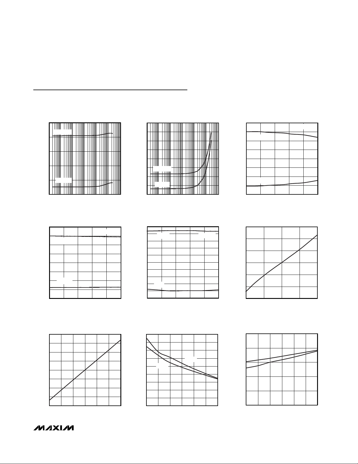
Typical Operating Characteristics
(VCC= +3.3V, C1 = C2 = 1.0µF, C3 = C4 = C5 = 3.3µF, TA= +25°C, unless otherwise noted.)
-8
-6
-4
-2
0
2
4
6
8
-40 -15 10 35 60 85
V.28 LOADED OUTPUT VOLTAGE
vs. TEMPERATURE
MAX3171 toc04
TEMPERATURE (°C)
OUTPUT VOLTAGE (V)
V
OUT+
V
OUT-
RL = 3k
Ω
-5
-2
-3
-4
-1
0
1
2
3
4
5
-40 10-15 356085
V.10 LOADED OUTPUT VOLTAGE
vs. TEMPERATURE
MAX3171 toc05
TEMPERATURE (°C)
OUTPUT VOLTAGE (V)
V
OUT+
V
OUT-
RL = 450
Ω
-0.3
-0.1
-0.2
0.1
0
0.2
0.3
-10 0-5 5 10
V.10/V.11 RECEIVER INPUT CURRENT
vs. INPUT VOLTAGE
MAX3171 toc06
INPUT VOLTAGE (V)
INPUT CURRENT (mA)
-4
-3
-2
-1
0
1
2
3
4
-15 -5-10 0 5 10 15
V.28 RECEIVER INPUT CURRENT
vs. INPUT VOLTAGE
MAX3171 toc07
INPUT VOLTAGE (V)
INPUT CURRENT (mA)
0
4
2
10
8
6
16
14
12
18
0 1000500 1500 2000 2500 3000
V.28 SLEW RATE
vs. LOAD CAPACITANCE
MAX3171toc11
CAPACITANCE (pF)
SLEW RATE (V/µs)
+SLEW
-SLEW
0
0.5
1.5
1.0
2.0
2.5
0 1000500 1500 2000 2500 3000
V.10 TRANSMITTER RISE AND FALL TIMES
vs. LOAD CAPACITANCE
MAX3171toc12
CAPACITANCE (pF)
RISE/FALL TIME (µs)
FALL
RISE
V.10/V.11 MODE SUPPLY CURRENT vs.
DATA RATE
250
FULL LOAD
200
150
100
SUPPLY CURRENT (mA)
50
NO LOAD
0
0.001 0.01 10k 100k0.1 1k 1000k
DATA RATE (kbps)
MAX3171 toc01
SUPPLY CURRENT (mA)
V.28 MODE SUPPLY CURRENT
vs. DATA RATE
80
70
60
50
40
30
FULL LOAD
20
NO LOAD
10
0
0.001 0.01 10k 100k0.1 1k 1000k
DATA RATE (kbps)
MAX3171 toc02
V.11 LOADED DIFFERENTIAL
OUTPUT VOLTAGE vs. TEMPERATURE
4
3
V
2
1
0
-1
OUTPUT VOLTAGE (V)
-2
-3
-4
OUT+
V
OUT-
-40 -15 10 35 60 85
TEMPERATURE (°C)
RL = 100
Ω
MAX3171 toc03
Page 6

MAX3171/MAX3173
+3.3V Multiprotocol 3Tx/3Rx
Software-Selectable Control Transceivers
6 _______________________________________________________________________________________
Typical Operating Characteristics (continued)
(VCC= +3.3V, C1 = C2 = 1.0µF, C3 = C4 = C5 = 3.3µF, TA= +25°C, unless otherwise noted.)
TIN2
TOUT2/
RIN2
ROUT2
5V/div
10µs/div
MAX3173 LOOPBACK SCOPE PHOTO
530A MODE (UNLOADED)
MAX3171 toc10
TIN
TOUT/
RIN
ROUT
5V/div
10µs/div
MAX3173 LOOPBACK SCOPE PHOTO
V.11 MODE (UNLOADED)
MAX3171 toc08
TIN
TOUT/
RIN
ROUT
5V/div
10µs/div
MAX3171 LOOPBACK SCOPE PHOTO
V.28 MODE (R
L
= 3kΩ)
MAX3171 toc09
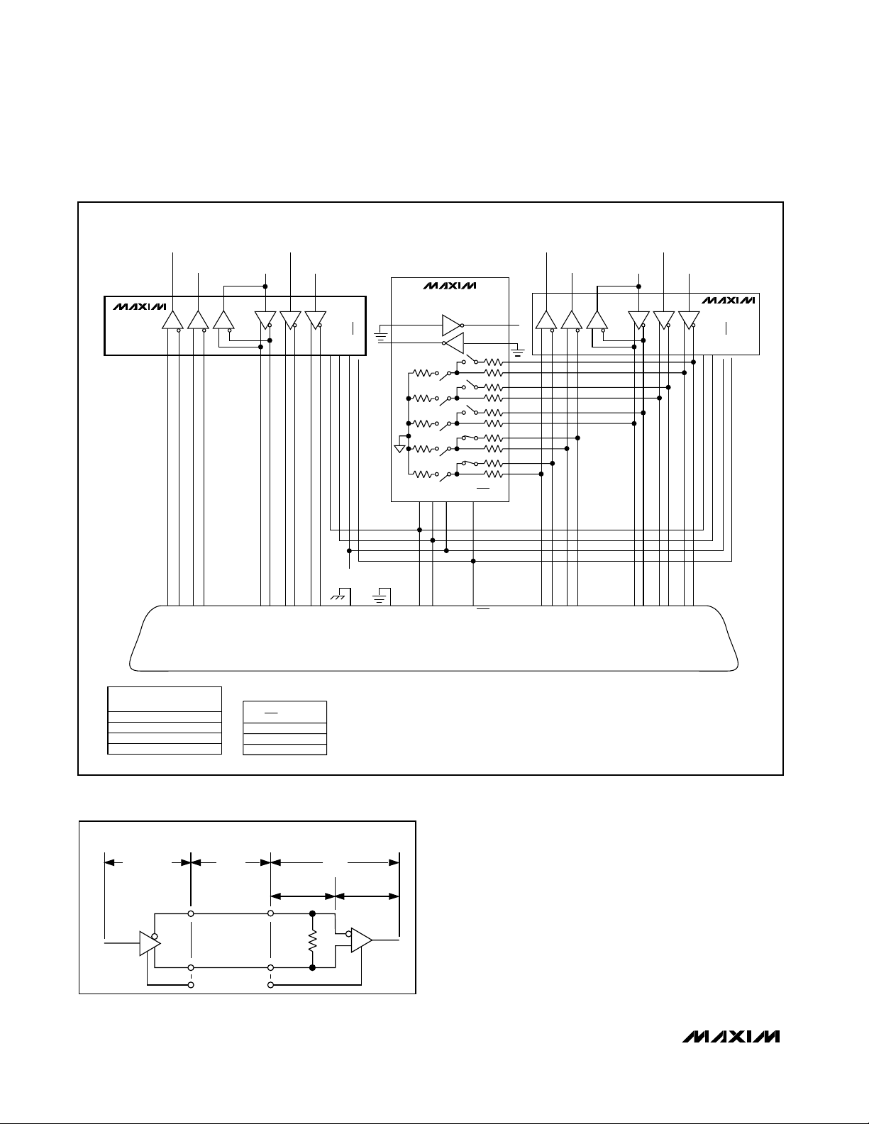
Figure 1. V.11 DC Test Circuit
Figure 2. V.11 AC Test Circuit
Test Circuits
V
OD
R
100Ω
V
R
OC
100pF
RxTx
50pF
100pF
Page 7

MAX3171/MAX3173
+3.3V Multiprotocol 3Tx/3Rx
Software-Selectable Control Transceiver
_______________________________________________________________________________________ 7
Pin Description
Figure 3. V.10/V.28 Driver Test Circuit
Figure 4. V.10/V.28 Receiver Test Circuit
Test Circuits (continued)
Tx
C
L
PIN NAME FUNCTION
1V+
2 C2+
3C2-
4V-
5, 6, 7 T_IN Transmitter CMOS Inputs (T1IN, T2IN, T3IN)
Positive Supply Generated by the Charge Pump (connect to V+ pin of MAX3172/MAX3174).
Bypass V+ to ground with a 3.3µF ceramic capacitor.
Positive Terminal of the Inverting Charge-Pump Capacitor. Connect C2+ to C2- with a 1µF
ceramic capacitor.
Negative Terminal of the Inverting Charge-Pump Capacitor. Connect C2+ to C2- with a 1µF
ceramic capacitor.
Negative Supply Generated by the Charge Pump (connect to V- pin of MAX3172/MAX3174).
Bypass V- to ground with a 3.3µF ceramic capacitor.
R
L
Tx Rx
50pF
8, 9, 10 R_OUT Receiver CMOS Outputs (R1OUT, R2OUT, R3OUT)
11, 12, 13 M_
14 DCE/DTE
15, 18 R_INB Noninverting Receiver Inputs (R3INB, R2INB)
16, 17 R_INA Inverting Receiver Inputs (R3INA, R2INA)
19 T3OUTB/R1INB Noninverting Transmitter Output/Noninverting Receiver Input
20 T3OUTA/R1INA Inverting Transmitter Output/Inverting Receiver Input
21, 23 T_OUTB Noninverting Transmitter Outputs (T2OUTB, T1OUTB)
22, 24 T_OUTA Inverting Transmitter Outputs (T2OUTA, T1OUTA)
25 C1-
26 GND Ground
27 V
28 C1+ Positive Terminal of the Voltage-Doubler Charge-Pump Capacitor. Connect C1+ to C1- with a
CC
Mode Select Inputs (M0, M1, M2). Internally pulled up to V
information.
DCE/DTE Mode Select Input. Logic level high selects DCE interface; logic level low selects
DTE interface. Internally pulled up to V
Negative Terminal of the Voltage-Doubler Charge-Pump Capacitor. Connect C1+ to C1- with
a 1µF ceramic capacitor.
+3.3V Supply Voltage (±5%). Bypass VCC to ground with a 3.3µF ceramic capacitor.
1µF ceramic capacitor.
CC
.
. See Table 1 for detailed
CC
Page 8

MAX3171/MAX3173
+3.3V Multiprotocol 3Tx/3Rx
Software-Selectable Control Transceivers
8 _______________________________________________________________________________________
Detailed Description
The MAX3171/MAX3173 are three-driver/three-receiver
multiprotocol transceivers that operate from a single
+3.3V supply. The MAX3171/MAX3173, along with the
MAX3170 and MAX3172/MAX3174, form a complete
software-selectable DTE or DCE interface port that supports the V.28 (RS-232), V.10/V.11 (RS-449, V.36, EIA530, EIA-530-A, X.21, RS-423), and V.35 protocols. The
MAX3171/MAX3173 carry the control signals, while the
MAX3170 transceiver carries the high-speed clock and
data signals. The MAX3172/MAX3174 provide termination for the clock and data signals and have an extra
transceiver for applications requiring four transceivers
for control handshaking.
The MAX3171/MAX3173 feature a 2mA no-cable mode,
true fail-safe operation, and thermal shutdown circuitry.
Thermal shutdown protects the drivers against excessive power dissipation. When activated, the thermal
shutdown circuitry places the driver outputs into a highimpedance state.
Mode Selection
The state of mode select pins M0, M1, and M2 determines
which serial interface protocol is selected (Table 1). The
state of the DCE/DTE input determines whether the transceivers will be configured as a DTE serial port or a DCE
serial port. When the DCE/DTE input is logic HIGH, driver T3 is activated and receiver R1 is disabled. When
the DCE/DTE input is logic LOW, driver T3 is disabled
and receiver R1 is activated. M0, M1, M2, and
DCE/DTE are internally pulled up to V
CC
to ensure logic
HIGH if left unconnected.
The MAX3171/MAX3173’s mode can be selected
through software control of the M0, M1, M2, and
DCE/DTE inputs. Alternatively, the mode can be selected by shorting the appropriate combination of mode
control inputs to GND (the inputs left floating will be
internally pulled up to V
CC
). If the M0, M1, and M2
mode inputs are all unconnected, the MAX3171/
MAX3173 will enter no-cable mode.
Table 1. Mode Selection
Figure 5. Charge-Pump Connections
Z = High impedance
PROTOCOL
V.11 0 0 0 0 V.11 V.11 Z V.11 V.11 V.11
RS-530A 0 0 1 0 V.11 V.10 Z V.11 V.10 V.11
RS-530 0 1 0 0 V.11 V.11 Z V.11 V.11 V.11
X.21 0 1 1 0 V.11 V.11 Z V.11 V.11 V.11
V.35 1 0 0 0 V.28 V.28 Z V.28 V.28 V.28
RS-449/V.36 1 0 1 0 V.11 V.11 Z V.11 V.11 V.11
V.28/RS-232 1 1 0 0 V.28 V.28 Z V.28 V.28 V.28
No cable 1 1 1 0 ZZZZZZ
V.11 0 0 0 1 V.11 V.11 V.11 Z V.11 V.11
RS-530A 0 0 1 1 V.11 V.10 V.11 Z V.10 V.11
RS-530 0 1 0 1 V.11 V.11 V.11 Z V.11 V.11
X.21 0 1 1 1 V.11 V.11 V.11 Z V.11 V.11
V.35 1 0 0 1 V.28 V.28 V.28 Z V.28 V.28
RS-449/V.36 1 0 1 1 V.11 V.11 V.11 Z V.11 V.11
V.28/RS-232 1 1 0 1 V.28 V.28 V.28 Z V.28 V.28
No cable 1 1 1 1 ZZZZZZ
M2 M1 M0 DCE/DTE T1 T2 T3 R1 R2 R3
LOGIC INPUTS TRANSMITTERS RECEIVERS
MAX3171
1
MAX3173
C3
3.3µF
3.3µF
C2
1µF
C4
V+
2
C2+
3
C2-
4
V-
C1+
V
GND
C1-
28
27
CC
C5
26
3.3µF
25
C1
1µF
Page 9

MAX3171/MAX3173
+3.3V Multiprotocol 3Tx/3Rx
Software-Selectable Control Transceiver
_______________________________________________________________________________________ 9
No-Cable Mode
The MAX3171/MAX3173 enter no-cable mode when the
mode select pins are left unconnected or tied HIGH
(M0 = M1 = M2 = 1). In this mode, the multiprotocol drivers and receivers are disabled and the supply current
is less than 8mA. The receiver outputs enter a highimpedance state in no-cable mode, which allows these
output lines to be shared with other receivers (the
receiver outputs have an internal pullup resistor to pull
the outputs HIGH if not driven). Also, in no-cable mode,
the transmitter outputs enter a high-impedance state,
so these output lines can be shared with other devices.
Dual Charge-Pump Voltage Converter
The MAX3171/MAX3173 internal power supply consists
of a regulated dual charge pump that provides positive
and negative output voltages from a +3.3V supply. The
charge pump operates in discontinuous mode: If the output voltage is less than the regulated voltage, the charge
pump is enabled; if the output voltage exceeds the regulated voltage, the charge pump is disabled. Each charge
pump requires a flying capacitor (C1, C2) and a reservoir capacitor (C3, C4) to generate the V+ and V- supplies. See Figure 5 for charge-pump connections.
The charge pump is designed to supply V+ and Vpower to the MAX3172/MAX3174 in addition to the
MAX3171/MAX3173 internal transceivers. Connect the
MAX3172/MAX3174 V+ and V- terminals to the
MAX3171/MAX3173 V+ and V- terminals, respectively.
Fail-Safe
The MAX3171/MAX3173 guarantee a logic HIGH
receiver output when the receiver inputs are shorted or
open, or when they are connected to a terminated
transmission line with drivers disabled. The V.11 receiver threshold is set between -25mV and -200mV to guarantee fail-safe operation. If the differential receiver input
voltage (B - A) is ≥ -25mV, R_OUT is logic HIGH. In the
case of a terminated bus with all transmitters disabled,
the receiver’s differential input voltage is pulled to 0 by
the termination. With the MAX3171/MAX3173 receiver
thresholds, this results in R_OUT logic HIGH with a
25mV (min) noise margin.
The V.10 receiver threshold is set between +25mV and
+300mV. If the V.10 receiver input voltage is ≤ +25mV,
ROUT is logic HIGH. The V.28 receiver threshold is set
between 0.8V and 2.0V. If the receiver input voltage is
≤ 0.8V, ROUT is logic HIGH. In the case of a terminated
bus with transmitters disabled, the V.10/V.28 receiver’s
input voltage is pulled to ground by the termination.
With the MAX3172/MAX3174 receiver thresholds, this
results in R_OUT logic HIGH.
Applications Information
Capacitor Selection
The capacitors used for the charge pumps, as well as
the supply bypassing, should have a low-ESR and lowtemperature coefficient. Multilayer ceramic capacitors
with an X7R dielectric offer the best combination of performance, size, and cost. The flying capacitors (C1,
C2) should have a value of 1µF, while the reservoir
capacitors (C3, C4) and bypass capacitor (C5) should
have a minimum value of 3.3µF (Figure 5). To reduce
the ripple present on the transmitter outputs, capacitors
C3, C4, and C5 can be increased. Do not increase the
value of C1 and C2.
Local Loopback Control Signal
For applications that require the use of local loopback
(LL) signal routing, an extra transceiver is available for
use on the MAX3172/MAX3174 multiprotocol termination network device.
Cable-Selectable Mode
Figure 6 shows a cable-selectable mulitprotocol interface. The mode control lines (M0, M1, M2, and
DCE/DTE) are wired to the DB-25 connector. To select
the serial interface mode, the appropriate combinations
of M0, M1, M2, and DCE/DTE are grounded within the
cable wiring. The control lines that are not grounded
are pulled high by the internal pullups on the MAX3170.
The serial interface protocol of the MAX3171/MAX3173
(MAX3170 and MAX3172/MAX3174) is now selected
based on the cable connected to the DB-25 interface.
V.11 (RS-422) Interface
As shown in Figure 7, the V.11 protocol is a fully balanced differential interface. The V.11 driver generates
±2V (min) between nodes A and B when 100Ω (min)
resistance is presented at the load. The V.11 receiver is
sensitive to ±200mV differential signals at the receiver
inputs A’ and B’. The V.11 receiver input must comply
with the impedance curve of Figure 8 and reject common-mode signals up to ±7V developed across the
cable (referenced from C to C’ in Figure 7).
The MAX3171/MAX3173 V.11 mode receiver has a differential threshold between -200mV and -25mV to
ensure that the receiver has proper fail-safe operation
(see Fail-Safe). To aid in rejecting system noise, the
MAX3171/MAX3173 V.11 receiver has a 15mV (typ)
hysteresis. Switch S3 in Figure 9 is open in V.11 mode
to disable the V.28 5kΩ termination at the inverting
receiver input. Because the control signals are slow
(64kbps), 100Ω termination resistance is generally not
required for the MAX3171/MAX3173.
Page 10
MAX3171/MAX3173
+3.3V Multiprotocol 3Tx/3Rx
Software-Selectable Control Transceivers
10 ______________________________________________________________________________________
V.10 Interface
The V.10 interface (Figure 10) is an unbalanced singleended interface capable of driving a 450Ω load. The
V.10 driver generates a ±4V (min) V
ODO
voltage across
A' and C' when unloaded and a minimum of ±0.9
✕
V
ODO
voltage with a 450Ω load. The V.10 receiver input
trip threshold is defined between +300mV and -300mV
with the input impedance characteristic shown in
Figure 8.
The MAX3171/MAX3173 V.10 mode receiver has a
threshold between +25mV and +300mV to ensure that
the receiver has proper fail-safe operation (see Fail-
Figure 6. Cable-Selectable Multiprotocol DCE/DTE Port
Figure 7. Typical V.11 Interface
MAX3171
MAX3173
CTS(DTE)
RTS(DCE)
DSR(DTE)
DTR(DCE)
R2R3
R1
DCD(DTE)
DCD(DCE)
D3
DTR(DTE)
DSR(DCE)
D2
RTS(DTE)
CTS(DCE)
D1
13 5 10 8 22 6 23 20 19 4 1 7 18 21 25 16 3 9 17 12 15 11 24 14 2
DTE
CTS B
CTS A
DSR
DCE
RTS B
RTS A
DSR
DTR B
DTR A
DCD
DCD
DCD
DCD
DTR B
DSR
DTR A
DSR
RTS B
CTS B
RTS A
CTS A
M1M2M0
V
CC
SHIELD
DCE/DTE
SG
DB-25 CONNECTOR
MAX3172
MAX3174
R4
M2M1M0
M1M0
D4
DCE/DTE
DCE/DTE
RXD(DTE)
TXD(DCE)
RXD
TXD B
RXC(DTE)
SCTE(DCE)
R2R3
RXD
RXC
TXD A
SCTE B
R1
RXC
SCTE A
TXC(DTE)
TXC(DCE)
D3
TXC B
TXC B
SCTE(DTE)
RXC(DCE)
TXC A
SCTE B
RXC
TXC A
TXD(DTE)
RXD(DCE)
D1D2
TXD B
SCTE A
RXC
RXD
TXD A
RXD
MAX3170
M1M2M0
DCE/DTE
CABLE WIRING FOR
MODE SELECTION
MODE
V.35
RS-449, V.36
RS-232
PIN 18
PIN 7
N.C.
PIN 7
PIN 21
PIN 7
PIN 7
N.C.
CABLE WIRING FOR
DCE/DTE SELECTION
MODE
DTE
DCE
PIN 25
PIN 7
N.C.
GENERATOR
BALANCED
INTERCONNECTING
CABLE
A
B
C
CABLE
TERMINATION
A′
100Ω
MIN
B′
C′
LOAD
RECEIVER
Page 11

MAX3171/MAX3173
+3.3V Multiprotocol 3Tx/3Rx
Software-Selectable Control Transceiver
______________________________________________________________________________________ 11
Figure 12. V.28 Termination and Internal Resistance Networks
Figure 11. V.10 Internal Resistance Network
Figure 10. Typical V.10/V.28 Interface
Figure 9. V.11 Termination and Internal Resistance Networks
Figure 8. Receiver Input Impedance Curve
I
-10V
-3.25mA
Z
-3V
+3V
3.25mA
V
+10V
A′
A
R5
30kΩ
R8
5kΩ
S3
B
B′
C′
GND
R4
30kΩ
10kΩ
R6
R7
10kΩ
MAX3171
MAX3173
RECEIVER
UNBALANCED
INTERCONNECTING
GENERATOR
CABLE
TERMINATION
A
A′
CABLE
LOAD
RECEIVER
A
A
′
R5
30k
30k
S4
Ω
R6
10k
Ω
R7
10k
R4
Ω
Ω
S5
Z
B
′
C
′
R8
5k
Ω
S3
B
GND
A
A
′
R5
30k
Ω
R8
5k
Ω
S3
B
B
′
30k
R6
10k
Ω
R7
10k
Ω
R4
Ω
MAX3171
MAX3173
RECEIVER
MAX3171
MAX3173
RECEIVER
C
C
′
C′
GND
Page 12

MAX3171/MAX3173
+3.3V Multiprotocol 3Tx/3Rx
Software-Selectable Control Transceivers
12 ______________________________________________________________________________________
Safe). To aid in rejecting system noise, the
MAX3171/MAX3173 V.10 receiver has 15mV (typ) hysteresis. Switch S3 in Figure 11 is open in V.10 mode to
disable the 5kΩ V.28 termination at the receiver input.
Switch S4 is closed, and switch S5 is open to internally
ground the receiver B input.
V.28 Interface
The V.28 interface is an unbalanced single-ended interface (Figure 12). The V.28 generator provides ±5V
(min) across the load impedance between A’ and C’.
The V.28 standard specifies input trip points at ±3V.
The MAX3171/MAX3173 V.28 mode receiver has a
threshold between +0.8V and +2.0V to ensure that the
receiver has proper fail-safe operation (see Fail-Safe). To
aid in rejecting system noise, the MAX3171/MAX3173
V.28 receiver has a 500mV (typ) hysteresis. Switch S3 in
Figure 12 is closed in V.28 mode to enable the 5kΩ V.28
termination at the receiver input.
Receiver Glitch Rejection
To facilitate operation in an unterminated or otherwise
noisy system, the MAX3171 features 10µs of receiver
input glitch rejection in V.10, V.11, and V.28 modes.
The glitch rejection circuitry blocks the reception of
high-frequency noise (tB< 5µs) while receiving a lowfrequency signal (tB> 15µs), allowing glitch-free operation in unterminated systems at up to 64kbps. The
MAX3173 does not have this feature and can be operated at data rates up to 240kbps if properly terminated.
DTE vs. DCE Operation
Figure 13 shows a DCE or DTE controller-selectable
interface. The DCE/DTE input switches the port’s mode
of operation. A logic high selects DCE, which enables
Figure 13. Multiprotocol DCE/
DTE
Port
MAX3171
MAX3173
CTS(DTE)
RTS(DCE)
DSR(DTE)
DTR(DCE)
R2R3
R1
DCD(DTE)
DCD(DCE)
D3
DTR(DTE)
DSR(DCE)
D2
RTS(DTE)
CTS(DCE)
D1
13 5 10 8 22 6 23 20 19 4 1 7 18 16 3 9 17 12 15 11 24 14 2
DTE
CTS B
CTS A
DSR B
DSR A
DCE
RTS B
RTS A
DTR B
DTR A
DCD B
DCD A
DCD B
DCD A
DTR B
DTR A
DSR B
DSR A
RTS B
CTS B
RTS A
CTS A
M1M2M0
DCE/DTE
SHIELD
RXD(DTE)
TXD(DCE)
LL(DTE)
LL(DCE)
MAX3172
MAX3174
R4
D4
DCE/DTE
M2M1M0
SG
LL A
DB-25 CONNECTOR
LL A
RXC(DTE)
SCTE(DCE)
RXD B
RXD A
TXD B
TXD A
R2R3
RXC B
SCTE B
R1
RXC A
SCTE A
TXC(DTE)
TXC(DCE)
D3
TXC B
TXC B
SCTE(DTE)
RXC(DCE)
TXC A
SCTE B
TXC A
RXC B
TXD(DTE)
RXD(DCE)
D1D2
TXD B
SCTE A
RXC A
RXD B
TXD A
RXD A
MAX3170
M1M2M0
M1M2M0
DCE/DTE
DCE/DTE
Page 13

driver 3 on the MAX3171/MAX3173, driver 3 on the
MAX3170, and driver 4 on the MAX3172/MAX3174. A
logic low selects DTE, which enables receiver 1 on the
MAX3171/MAX3173, receiver 1 on the MAX3170, and
receiver 4 on the MAX3172/MAX3174.
This application requires only one DB-25 connector. See
Figure 13 for complete signal routing in DCE and DTE
modes. For example, driver 3 routes the DCD (DCE) signal to pins 22 and 6 in DCE mode, while in DTE mode,
receiver 1 routes pins 22 and 6 to DCD (DTE).
Complete Multiprotocol X.21 Interface
Figure 14 shows a complete DCE-to-DTE interface
operating in X.21 mode. The MAX3171/MAX3173 generate the control signals, and the MAX3170 is used to
generate the clock and data signals. The MAX3172/
MAX3174 generate local loopback and are used to terminate the clock and data signals to support the V.11
protocol for cable termination. The control signals do
not need external termination.
MAX3171/MAX3173
+3.3V Multiprotocol 3Tx/3Rx
Software-Selectable Control Transceiver
______________________________________________________________________________________ 13
Figure 14. DCE-to-DTE X.21 Interface
SERIAL
CONTROLLER
DTE
MAX3170
MAX3172
MAX3174
MAX3174
DCE
MAX3170MAX3172
SERIAL
CONTROLLER
TXD
SCTE
TXC
RXC
RXD
RTS
DTR
DCD
D1
D2
D3
R1
R2
R3
LL
MAX3171
MAX3173
D1
D2
D3
R1
103Ω
103Ω
103Ω
D4
R4
SCTE
TXD
TXC
RXC
RXD
LL
RTS
DTR
DCD
103Ω
103Ω
R3
R2
R1
D3
D2
D1
R4
D4
MAX3171
MAX3173
R3
R2
R1
D3
TXD
SCTE
TXC
RXC
RXD
LL
RTS
DTR
DCD
DSR
CTS
R2
R3
DSR
CTS
D2
D1
DSR
CTS
Page 14

Compliance Testing
A European Standard EN 45001 test report is available
for the MAX3170–MAX3174 chipset. A copy of the test
report will be available from Maxim.
Pin Configuration
28
27
26
25
24
23
22
21
20
19
18
17
16
15
1
2
3
4
5
6
7
8
9
10
11
12
13
14
C1+
V
CC
GND
C1-
T1OUTA
T1OUTB
R3INB
T2OUTA
T2OUTB
T3OUTA/R1INA
T3OUTB/R1INB
R2INB
R2INA
R3INA
DCE/DTE
M2
M1
M0
R3OUT
R2OUT
R1OUT
T3IN
T2IN
T1IN
V-
C2-
C2+
V+
SSOP
TOP VIEW
MAX3171
MAX3173
Chip Information
TRANSISTOR COUNT: 1763
PROCESS: BiCMOS
MAX3171/MAX3173
+3.3V Multiprotocol 3Tx/3Rx
Software-Selectable Control Transceivers
14 ______________________________________________________________________________________
Page 15

Maxim cannot assume responsibility for use of any circuitry other than circuitry entirely embodied in a Maxim product. No circuit patent licenses are
implied. Maxim reserves the right to change the circuitry and specifications without notice at any time.
Maxim Integrated Products, 120 San Gabriel Drive, Sunnyvale, CA 94086 408-737-7600 ____________________ 15
© 2001 Maxim Integrated Products Printed USA is a registered trademark of Maxim Integrated Products.
Package Information
MAX3171/MAX3173
+3.3V Multiprotocol 3Tx/3Rx
Software-Selectable Control Transceiver
SSOP.EPS
 Loading...