

Page 1
General Description
The MAX3160E/MAX3161E/MAX3162E are programmable RS-232/RS-485/RS-422 multiprotocol transceivers.
The MAX3160E/MAX3161E are pin programmable as a
2Tx/2Rx RS-232 interface or a single RS-485/RS-422
transceiver. The MAX3162E is configured as a 2Tx/2Rx
RS-232 interface, and a single RS-485/RS-422 transceiver simultaneously.
The MAX3160E/MAX3161E/MAX3162E feature enhanced
electrostatic discharge (ESD) protection. All of the transmitter outputs and receiver inputs are protected to ±15kV
using the Human Body Model.
All devices incorporate a proprietary low-dropout transmitter output stage, and an on-board dual charge pump
to allow RS-232- and RS-485-/RS-422-compliant performance from a +3V to +5.5V supply. The receivers feature
true fail-safe circuitry that guarantees a logic-high receiver output when the receiver inputs are open or shorted.
These devices also feature pin-selectable transmitter
slew rates for RS-232 and RS-485/RS-422 modes. Slewrate limiting minimizes EMI and reduces reflections
caused by improperly terminated cables, allowing errorfree data transmission up to 250kbps. Disabling slew-rate
limiting allows these devices to transmit at data rates up
to 10Mbps in RS-485/RS-422 mode and up to 1Mbps in
RS-232 mode. The MAX3160E/MAX3161E/MAX3162E
feature a 10nA shutdown mode, short-circuit limiting, and
thermal shutdown circuitry to protect against excessive
power dissipation.
The MAX3160E/MAX3162E offer a flow-through pinout that facilitates board layout. The MAX3160E/
MAX3161E/MAX3162E are available in tiny SSOP packages and operate over the commercial and extended
temperature ranges.
________________________Applications
Point-of-Sales Equipment Peripherals
Industrial Controls Networking
RS-232 to RS-485 Security Systems
Interface Converters
Features
♦ Single Supply Operation from +3V to +5.5V
♦ ESD Protection
±15kV Human Body Model
♦ Pin-Selectable as 2Tx/2Rx RS-232 or Single
RS-485/RS-422 (MAX3160E/MAX3161E)
♦ 2Tx/2Rx RS-232 and Single RS-485/RS-422
(MAX3162E)
♦ Pin-Selectable RS-232/RS-485 Transmitter Slew
Rates Reduce EMI
♦ 10Mbps RS-485 and 1Mbps RS-232 Data Rates
♦ Pin-Selectable Half-Duplex or Full-Duplex
RS-485/RS-422 Operation (MAX3160E/MAX3161E)
♦ RS-485/RS-422 True Fail-Safe Receivers
♦ 10nA Shutdown Supply Current
♦ 1/8-Unit Load Allows up to 256 Transceivers on
the Bus
MAX3160E/MAX3161E/MAX3162E
±15kV ESD-Protected, +3.0V to +5.5V, 10nA,
RS-232/RS-485/RS-422 Multiprotocol Transceivers
________________________________________________________________ Maxim Integrated Products 1
19-3580; Rev 0; 2/05
EVALUATION KIT
AVAILABLE
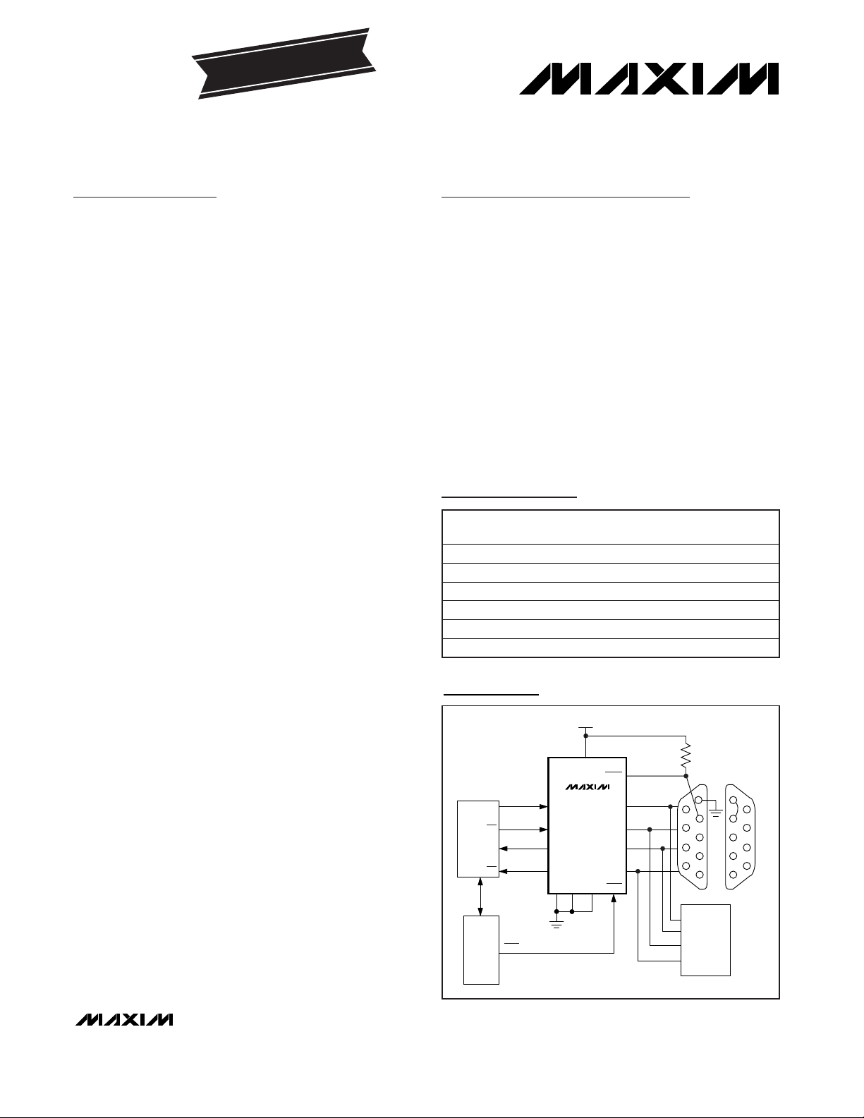
Typical Operating Circuit
Pin Configurations appear at end of data sheet.
Selector Guide appears at end of data sheet.
TX
V
CC
DI/T1IN
Z(B)/T1OUT
R1OUT
B/R1IN
GND FAST HDPLX SHDN
Y(A)/T2OUT
A/R2IN
CTS
13
10
DE485/T2IN
RTS
11
15
6
RO/R2OUT
RX
12
8
13
7
14
910
12
16
5
11
RJ45
DB9
SHDN
µP
SPI
MAX3100
RS-485/RS232
2
MAX3160E
+3V TO +5.5V
4
For price, delivery, and to place orders, please contact Maxim Distribution at 1-888-629-4642,
or visit Maxim’s website at www.maxim-ic.com.
Ordering Information
PART
TEMP RANGE
PIN-
PACKAGE
CODE
MAX3160ECAP
20 SSOP A20-2
MAX3160EEAP
20 SSOP A20-2
MAX3161ECAG
24 SSOP A24-3
MAX3161EEAG
24 SSOP A24-3
MAX3162ECAI
28 SSOP A28-1
MAX3162EEAI
28 SSOP A28-1
PACKAGE
0°C to +70°C
-40°C to +85°C
0°C to +70°C
-40°C to +85°C
0°C to +70°C
-40°C to +85°C
Page 2
MAX3160E/MAX3161E/MAX3162E
±15kV ESD-Protected, +3.0V to +5.5V, 10nA,
RS-232/RS-485/RS-422 Multiprotocol Transceivers
2 _______________________________________________________________________________________
ABSOLUTE MAXIMUM RATINGS
ELECTRICAL CHARACTERISTICS
(VCC= +3V to +5.5V, C1–C4 = 0.1µF when tested at +3.3V ±10%; C1 = 0.047µF and C2, C3, C4 = 0.33µF when tested at +5V±10%;
T
A
= T
MIN
to T
MAX
, unless otherwise noted. Typical values are at VCC= +3.3V and TA= +25°C.) (Note 2)
Stresses beyond those listed under “Absolute Maximum Ratings” may cause permanent damage to the device. These are stress ratings only, and functional
operation of the device at these or any other conditions beyond those indicated in the operational sections of the specifications is not implied. Exposure to
absolute maximum rating conditions for extended periods may affect device reliability.
Note 1: V+ and V- can have maximum magnitudes of 7V, but their absolute difference cannot exceed 13V.
V
CC
to GND..............................................................-0.3V to +6V
V+ to GND ................................................................-0.3V to +7V
V- to GND. ................................................................-7V to +0.3V
V+ - V- (Note 1)....................................................................+13V
Input Voltages
T1IN, T2IN, DI, DE485,
RE485, TE232, RE232, SHDN,
FAST, HDPLX, RS485/RS232 to GND. .................-0.3V to +6V
A, B, R1IN, R2IN to GND .................................................±25V
Output Voltages
T1OUT, T2OUT, Y, Z to GND (V
CC
= 0 or
SHDN = GND) ..............................................................±13.2V
T1OUT, T2OUT to GND (V
CC
= 5.5V and
SHDN = V
CC
) .....................................................-13.2V to +9V
R2OUT, R1OUT, RO to GND..................-0.3V to (V
CC
+ 0.3V)
Output Short-Circuit Duration
T1OUT, T2OUT, Y, Z ..............................................Continuous
Continuous Power Dissipation (T
A
= +70°C)
20-Pin SSOP (derate 8.0mW/°C above +70°C) ...........640mW
24-Pin SSOP (derate 8.0mW/°C above +70°C) ...........640mW
28-Pin SSOP (derate 9.1mW/°C above +70°C) ...........727mW
Operating Temperature Ranges
MAX316_CA_......................................................0°C to +70°C
MAX316_EA_ ...................................................-40°C to +85°C
Storage Temperature Range .............................-65°C to +150°C
Junction Temperature......................................................+150°C
Lead Temperature (soldering, 10s) .................................+300°C
PARAMETER
CONDITIONS
UNITS
DC CHARACTERISTICS
MAX3160E/MAX3161E, no load,
RS-485/ RS-232 = GND
1.2 2.8
MAX3160E/MAX3161E, no load,
RS-485/ RS-232 = V
CC
2.5 5.5
VCC Standby Current I
CC
MAX3162E, no load 3 6
mA
VCC Shutdown Current I
SHDN
SHDN = GND, receiver inputs open or
grounded
1µA
TRANSMITTER AND LOGIC INPUTS (DI, T1IN, T2IN, DE485, RRRREEEE444488885555, TE232, RRRREEEE222233332222, FAST, HDPLX, SHDN, RS-485/ RRRRSSSS----222233332222 )
Logic-Input Low V
IL
0.8 V
VCC = +3.3V 2.0
Logic-Input High V
IH
VCC = +5V 2.4
V
Logic-Input Leakage Current I
INL
±1µA
Transmitter Logic Hysteresis V
HYS
0.5 V
RS-232 AND RS-485/RS-422 RECEIVER OUTPUTS (R1OUT, R2OUT, RO)
Receiver Output-Voltage Low V
OL
I
OUT
= 2.5mA 0.4 V
Receiver Output-Voltage High V
OH
I
OUT
= -1.5mA V
CC
- 0.6 V
Receiver Output Short-Circuit
Current
I
OSR
0 ≤ VO ≤ V
CC
±85 mA
Receiver Output Leakage
Current
I
OZR
Receivers disabled
±1µA
SYMBOL
MIN TYP MAX
0.01
±0.01
±20
±0.05
Page 3
MAX3160E/MAX3161E/MAX3162E
±15kV ESD-Protected, +3.0V to +5.5V, 10nA,
RS-232/RS-485/RS-422 Multiprotocol Transceivers
_______________________________________________________________________________________ 3
ELECTRICAL CHARACTERISTICS (continued)
(VCC= +3V to +5.5V, C1–C4 = 0.1µF when tested at +3.3V ±10%; C1 = 0.047µF and C2, C3, C4 = 0.33µF when tested at +5V±10%;
T
A
= T
MIN
to T
MAX
, unless otherwise noted. Typical values are at VCC= +3.3V and TA= +25°C.) (Note 2)
PARAMETER
CONDITIONS
UNITS
RS-232 RECEIVER INPUTS (R1IN, R2IN)
Input Voltage Range -25
V
Logic-Input Low 0.8
V
CC
= +3.3V 2.0
Logic-input High
V
CC
= +5V 2.4
V
Input Hysteresis 0.5 V
VCC = +3.0V to 5.5V 3 5 7
Input Resistance
V
CC
= 0 6 11 16
kΩ
RS-485/RS-422 RECEIVER INPUTS (Note 3)
MAX3160E 48
Input Resistance R
IN
-7V < VCM < +12V
MAX3161E/
MAX3162E
96
kΩ
MAX3160E
V
CM
= -7V
Input Current I
IN
MAX3161E/MAX3162E
V
CM
= -7V
mA
Input Differential Threshold V
TH
-7V ≤ VCM ≤ +12V
-50 mV
Input Hysteresis ∆V
TH
30 mV
RS-232 TRANSMITTER OUTPUTS (T1OUT, T2OUT)
Output Voltage Swing
Both transmitter outputs loaded with 3kΩ
to GND
±5
V
Output Resistance VCC = V+ = V- = 0, T_OUT = ±2V
Ω
Output Short-Circuit Current I
SC
T_OUT = GND
±60 mA
MAX3160E
MAX3161E ±25
Output Leakage Current I
O
V
OUT
= ±9V
TE232 = GND or SHDN =
GND
MAX3162E ±25
µA
RS-485/RS-422 TRANSMITTER OUTPUTS (Y, Z)
R = 27Ω
(RS-485)
1.5
Differential Output Voltage V
OD
Figure 1
R = 50Ω
(RS-422)
2
V
Change in Magnitude of
Differential Output Voltage for
Complementary Output States
R = 27Ω or 50Ω, Figure 1 0.2 V
Common-Mode Output Voltage
V
OC
R = 27Ω or 50Ω, Figure 1 3 V
Change in Magnitude of
Common-Mode Output Voltage
for Complementary Output
States
R = 27Ω or 50Ω, Figure 1 0.2 V
SYMBOL
VCM = +12V 0.25
VCM = +12V 0.125
MIN TYP MAX
-200
+25
-0.15
-0.075
|∆VOD|
|∆VOC|
300 10M
±5.4
±30
±125
Page 4
MAX3160E/MAX3161E/MAX3162E
±15kV ESD-Protected, +3.0V to +5.5V, 10nA,
RS-232/RS-485/RS-422 Multiprotocol Transceivers
4 _______________________________________________________________________________________
PARAMETER
CONDITIONS
UNITS
Output Short-Circuit Current I
SC
VY or VZ = -7V to +12V
mA
MAX3160E
MAX3161E ±25
Output Leakage Current
I
O
VY or VZ = -7V or +12V,
DE485 = GND or SHDN =
GND
MAX3162E ±25
µA
RS-232 TRANSMITTER TIMING CHARACTERISTICS (SLOW MODE, FAST = GND, 250kbps, one transmitter switching)
Maximum Data Rate RL = 3kΩ, CL = 1000pF
kbps
Transmitter Skew
RL = 3kΩ, CL = 150pF, Figure 6 25 ns
CL = 150pF
to 1000pF
630
Transition-Region Slew Rate
V
CC
= +3.3V, TA = +25°C,
R
L
= 3kΩ to 7kΩ,
measured from +3.0V to
-3.0V or -3.0V to +3.0V
C
L
= 150pF
to 2500pF
430
V/µs
RS-232 TRANSMITTER TIMING CHARACTERISTICS (FAST MODE, FAST = VCC, 1Mbps, one transmitter switching)
VCC = +3V to +4.5V, RL = 3kΩ, CL = 250pF 1
Maximum Data Rate
V
CC
= +4.5V to +5.5V, RL = 3kΩ,
C
L
= 1000pF
1
Mbps
Transmitter Skew
RL = 3kΩ, CL = 150pF, Figure 6 10 ns
13 150
Transition-Region Slew Rate
V
CC
= +3.3V, TA = +25°C, R
L
= 3kΩ to 7kΩ, CL = 150pF to
1000pF, measured from +3.0V
to -3.0V or -3.0V to +3.0V
MAX3161E
24 150
V/µs
RS-232 RECEIVER TIMING CHARACTERISTICS
Receiver Propagation Delay
R_IN to R_OUT, CL = 15pF, Figure 5
µs
Receiver Output Enable Time
CL = 50pF, Figures 2, 10, MAX3162E
ns
Receiver Output Disable Time
CL = 15pF, Figures 2, 10, MAX3162E
ns
Receiver Skew
CL = 50pF, Figure 5
ns
RS-485/RS-422 DRIVER TIMING CHARACTERISTICS (SLOW MODE, FAST = GND, 250kbps)
Differential Driver Propagation
Delay
t
DPHL
,
t
DPLH
R
DIFF
= 54Ω, CL = 50pF, Figures 3, 7
800 ns
Differential Driver Rise and Fall
Time
t
DR,
t
DF
R
DIFF
= 54Ω, CL = 50pF, Figures 3, 7
800 ns
Differential Driver Propagation
Delay Skew
R
DIFF
= 54Ω, CL = 50pF, Figures 3, 7 200 ns
Driver Output Enable Time
CL = 50pF, Figures 4, 8
900 ns
Driver Output Disable Time
CL = 50pF, Figures 4, 8
400 ns
ELECTRICAL CHARACTERISTICS (continued)
(VCC= +3V to +5.5V, C1–C4 = 0.1µF when tested at +3.3V ±10%; C1 = 0.047µF and C2, C3, C4 = 0.33µF when tested at +5V±10%;
T
A
= T
MIN
to T
MAX
, unless otherwise noted. Typical values are at VCC= +3.3V and TA= +25°C.) (Note 2)
SYMBOL
t
TSKEW
MIN TYP MAX
±250
±125
250
t
TSKEW
t
PHL,tPLH
t
RZL,tRZH
t
RLZ,tRHZ
t
RSKEW
t
DSKEW
t
, t
DZH
t
, t
DLZ
DZL
DHZ
MAX3160E
MAX3162E
200 400
200 400
0.15
200
200
100
400
200
Page 5
MAX3160E/MAX3161E/MAX3162E
±15kV ESD-Protected, +3.0V to +5.5V, 10nA,
RS-232/RS-485/RS-422 Multiprotocol Transceivers
_______________________________________________________________________________________ 5
PARAMETER
CONDITIONS
UNITS
RS-485/RS-422 DRIVER TIMING CHARACTERISTICS FAST MODE, FAST = VCC, 10Mbps)
Differential Driver Propagation
Delay
t
DPHL,
t
DPLH
R
DIFF
= 54Ω, CL = 50pF, Figures 3, 7 60 120 ns
Differential Driver Rise and Fall
Times
R
DIFF
= 54Ω, CL = 50pF, Figures 3, 7 10 25 ns
Differential Driver Propagation
Delay Skew
R
DIFF
= 54Ω, CL = 50pF, Figures 3, 7 10 ns
Driver Output Enable Time
CL = 50pF, Figures 4, 8
900 ns
Driver Output Disable Time
CL = 50pF, Figures 4, 8
400 ns
RS-485/RS-422 RECEIVER TIMING CHARACTERISTICS
Receiver Propagation Delay
t
RPLH
,
t
RPHL
CL = 15pF, Figures 9, 11 80 150 ns
Receiver Propagation Delay
Skew
CL = 15pF, Figures 9, 11 1 10 ns
Receiver Output Enable Time
MAX3162E, CL = 50pF, Figures 2, 10
ns
Receiver Output Disable Time
MAX3162E, CL = 15pF, Figures 2, 10
ns
ESD PROTECTION
R_IN, T_OUT, A, B, Y, Z Human Body Model
kV
ELECTRICAL CHARACTERISTICS (continued)
(VCC= +3V to +5.5V, C1–C4 = 0.1µF when tested at +3.3V ±10%; C1 = 0.047µF and C2, C3, C4 = 0.33µF when tested at +5V±10%;
T
A
= T
MIN
to T
MAX
, unless otherwise noted. Typical values are at VCC= +3.3V and TA= +25°C.) (Note 2)
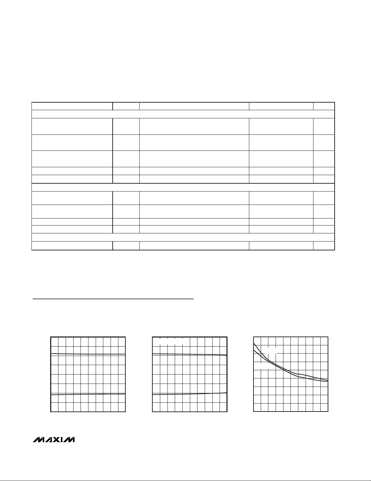
Typical Operating Characteristics
(VCC= +3.3V, 250kbps data rate, C
BYPASS
, C1, C2, C3, C4 = 0.1µF, all RS-232 transmitters (RS-232 mode) loaded with 3kΩ to
ground, TA= +25°C, unless otherwise noted.)
-10.00
-5.00
-7.50
-2.50
5.00
7.50
2.50
0
10.00
0 1000 2000 3000 4000 5000
RS-232 TRANSMITTER OUTPUT VOLTAGE
vs. LOAD CAPACITANCE (FAST = GND)
MAX3160E toc01
LOAD CAPACITANCE (pF)
TRANSMITTER OUTPUT VOLTAGE (V)
-10.00
-5.00
-7.50
-2.50
5.00
7.50
2.50
0
10.00
0 500 1000 1500 2000 2500
RS-232 TRANSMITTER OUTPUT VOLTAGE
vs. LOAD CAPACITANCE (FAST = V
CC
)
MAX3160E toc02
LOAD CAPACITANCE (pF)
TRANSMITTER OUTPUT VOLTAGE (V)
DATA RATE = 1Mbps
0
4
2
8
6
10
12
16
14
18
0 1000 2000 3000 4000 5000
RS-232 TRANSMITTER SLEW RATE
vs. LOAD CAPACITANCE (FAST = GND)
MAX3160E toc03
LOAD CAPACITANCE (pF)
SLEW RATE (V/µs)
RISING
FALLING
Note 2: All currents into the device are positive. All currents out of the device are negative.
Note 3: Applies to A, B for MAX3162E and MAX3160E/MAX3161E with HDPLX = GND, or Y, Z for MAX3160E/MAX3161E with
HDPLX = V
CC.
SYMBOL
tDR, t
DF
t
DSKEW
t
DZH,tDZL
t
DHZ,tDLZ
t
RSKEW
t
, t
RZL
RZH
t
, t
RLZ
RHZ
MIN TYP MAX
400
200
100
100
±15
Page 6
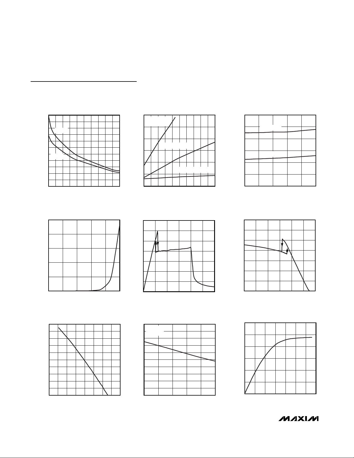
MAX3160E/MAX3161E/MAX3162E
±15kV ESD-Protected, +3.0V to +5.5V, 10nA,
RS-232/RS-485/RS-422 Multiprotocol Transceivers
6 _______________________________________________________________________________________
0
50
150
100
200
250
-40 10-15 35 60 85
SHUTDOWN CURRENT
vs. TEMPERATURE
MAX3160E toc07
TEMPERATURE (°C)
SHUTDOWN CURRENT (nA)
0
40
20
80
60
120
100
140
0462 8 10 12
RS-485/RS-422 OUTPUT CURRENT
vs. DRIVER-OUTPUT LOW VOLTAGE
MAX3160E toc08
OUTPUT LOW VOLTAGE (V)
OUTPUT CURRENT (mA)
0
40
20
80
60
120
100
140
-7 -3 -1-5 135
RS-485/RS-422 OUTPUT CURRENT
vs. DRIVER-OUTPUT LOW VOLTAGE
MAX3160E toc09
OUTPUT LOW VOLTAGE (V)
OUTPUT CURRENT (mA)
0
20
10
40
30
60
50
70
90
80
100
0 1.0 1.50.5 2.0 2.5 3.0 3.5 4.0
RS-485/RS-422 DRIVER OUTPUT CURRENT
vs. DIFFERENTIAL OUTPUT VOLTAGE
MAX3160E toc10
OUTPUT LOW VOLTAGE (V)
OUTPUT CURRENT (mA)
2.0
2.3
2.2
2.1
2.4
2.5
2.6
2.7
2.8
2.9
3.0
-40 10-15 35 60 85
RS-485/RS-422 DRIVER DIFFERENTIAL
OUTPUT vs. TEMPERATURE
MAX3160E toc11
TEMPERATURE (°C)
OUTPUT VOLTAGE (V)
R
DIFF
= 100Ω
FIGURE 1
0
10
5
20
15
25
30
0 1.5 2.00.5 1.0 2.5 3.0 3.5
RECEIVER OUTPUT CURRENT vs. RECEIVER-
OUTPUT LOW VOLTAGE
MAX3160E toc12
OUTPUT LOW VOLTAGE (V)
OUTPUT CURRENT (mA)
Typical Operating Characteristics (continued)
(VCC= +3.3V, 250kbps data rate, C
BYPASS
, C1, C2, C3, C4 = 0.1µF, all RS-232 transmitters (RS-232 mode) loaded with 3kΩ to
ground, TA= +25°C, unless otherwise noted.)
0
20
10
50
40
30
60
70
100
90
80
110
0 400 800 1200 1600 2000
RS-232 TRANSMITTER SLEW RATE
vs. LOAD CAPACITANCE (FAST = V
CC
)
MAX3160E toc04
LOAD CAPACITANCE (pF)
SLEW RATE (V/µs)
RISING
FALLING
0
30
20
10
40
50
60
0 20001000 3000 4000 5000
OPERATING SUPPLY CURRENT
vs. LOAD CAPACITANCE WHEN
TRANSMITTING DATA (RS-232 MODE)
MAX3160E to05
LOAD CAPACITANCE (pF)
SUPPLY CURRENT (mA)
DATA RATE =
1Mbps
DATA RATE = 250kbps
DATA RATE = 20kbps
0
1.0
0.5
2.0
1.5
2.5
3.0
-40 10-15 35 60 85
MAX3160E/MAX3161E
NO-LOAD SUPPLY CURRENT
vs. TEMPERATURE
MAX3160E toc06
TEMPERATURE (°C)
SUPPLY CURRENT (mA)
RS-485 MODE
RS-232 MODE
Page 7
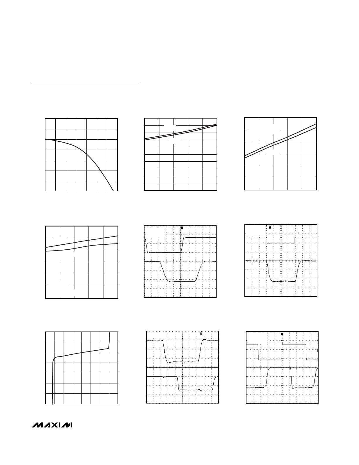
MAX3160E/MAX3161E/MAX3162E
±15kV ESD-Protected, +3.0V to +5.5V, 10nA,
RS-232/RS-485/RS-422 Multiprotocol Transceivers
_______________________________________________________________________________________ 7
0
30
20
10
40
50
60
70
80
90
100
-40 10-15 35 60 85
RS-485/RS-422 RECEIVER PROPAGATION
DELAY vs. TEMPERATURE
MAX3160E toc14
TEMPERATURE (°C)
PROPAGATION DELAY (ns)
RISING
FALLING
20
30
25
40
35
45
50
-40 10-15 35 60 85
RS-485/RS-422 DRIVER PROPAGATION DELAY
vs. TEMPERATURE (FAST = V
CC
)
MAX3160E toc15
TEMPERATURE (°C)
PROPAGATION DELAY (ns)
CL = 50pF
R
DIFF
= 54Ω
DATA RATE = 10Mbps
FALLING
RISING
100
200
150
300
250
350
400
-40 10-15 35 60 85
RS-485/RS-422 DRIVER PROPAGATION DELAY
vs. TEMPERATURE (FAST = GND)
MAX3160E toc16
TEMPERATURE (°C)
PROPAGATION DELAY (ns)
CL = 50pF
R
DIFF
= 54Ω
DATA RATE = 250kbps
FALLING
RISING
20ns/div
RS-485/RS-422 DRIVER PROPAGATION
(FAST = V
CC
, 10Mbps)
VY - V
Z
2V/div
DI
2V/div
MAX3160E toc17
CL = 50pF
R
DIFF
= 54
Ω
1.0µs/div
RS-485/RS-422 DRIVER PROPAGATION
(FAST = GND, 250kbps)
VY - V
Z
2V/div
DI
2V/div
MAX3160E toc18
CL = 50pF
R
DIFF
= 54
Ω
4ns/div
RS-485/RS-422 RECEIVER PROPAGATION
(FAST = V
CC
, 5Mbps)
VY - V
Z
2V/div
RO
2V/div
MAX3160E toc20
CL = 15pF
100ns/div
RS-485/RS-422 RECEIVER PROPAGATION
(FAST = V
CC
, 5Mbps)
VY - V
Z
2V/div
MAX3160E toc21
CL = 50pF
R
DIFF
= 54
Ω
DE485
2V/div
0
4
2
8
6
12
10
14
0 1.0 1.50.5 2.0 2.5 3.0 3.5
RECEIVER OUTPUT CURRENT
vs. RECEIVER-OUTPUT HIGH VOLTAGE
MAX3160E toc13
OUTPUT-HIGH VOLTAGE (V)
OUTPUT CURRENT (mA)
Typical Operating Characteristics (continued)
(VCC= +3.3V, 250kbps data rate, C
BYPASS
, C1, C2, C3, C4 = 0.1µF, all RS-232 transmitters (RS-232 mode) loaded with 3kΩ to
ground, TA= +25°C, unless otherwise noted.)
-1000
-800
-400
-600
0
200
-200
400
-20 -10 -5-15 0 5 101520
I-V OUTPUT IMPEDANCE CURVE
IN RS-232 SHUTDOWN MODE
MAX3160E toc19
OUTPUT VOLTAGE (V)
OUTPUT CURRENT (µA)
Page 8
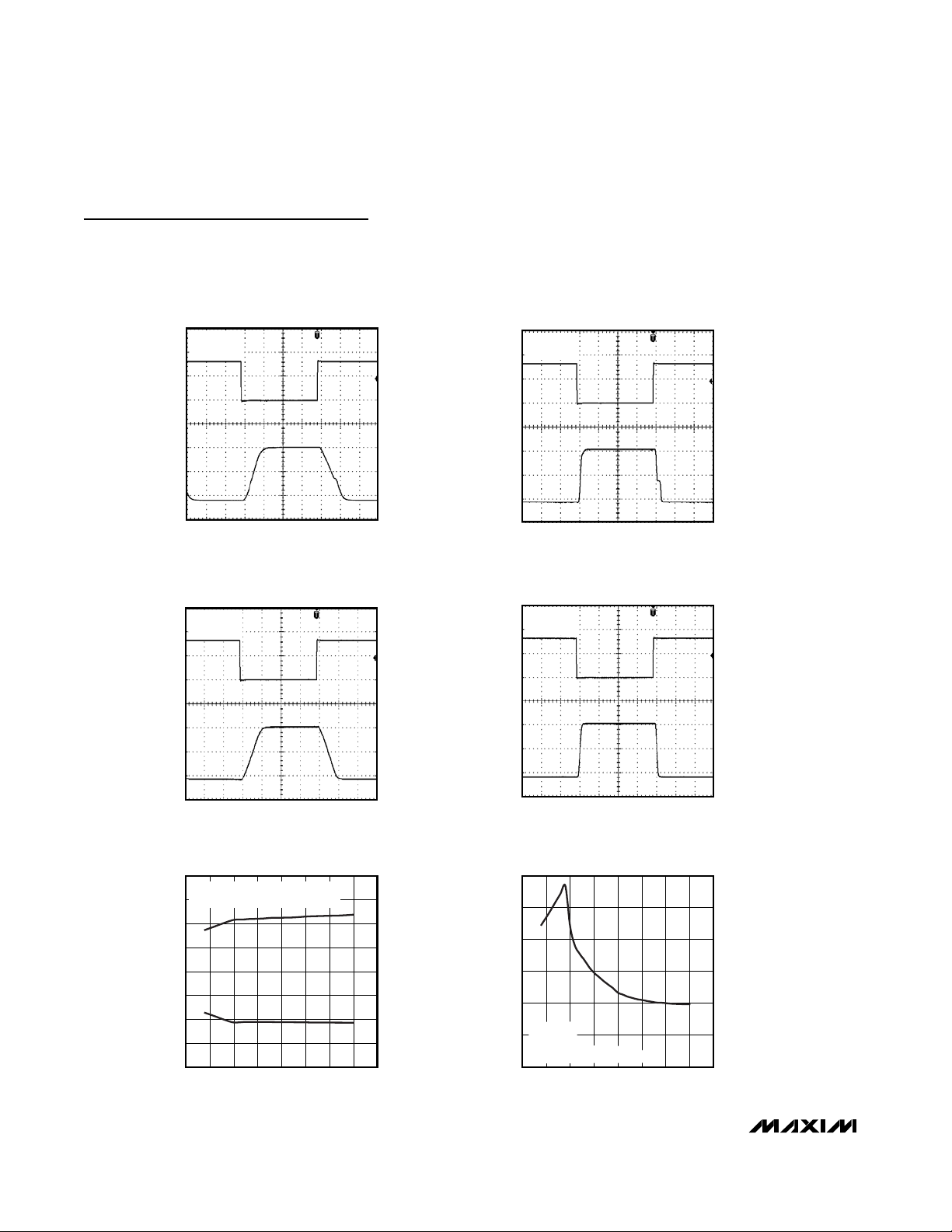
MAX3160E/MAX3161E/MAX3162E
±15kV ESD-Protected, +3.0V to +5.5V, 10nA,
RS-232/RS-485/RS-422 Multiprotocol Transceivers
8 _______________________________________________________________________________________
1.0µs/div
MAX3160E
RS-232 TRANSMITTER PROPAGATION
(FAST = GND, 250kbps)
T_OUT
5V/div
MAX3160E toc22
CL = 1000pF
R
L
= 7kΩ
DI
2V/div
1.0µs/div
MAX3160E
RS-232 TRANSMITTER PROPAGATION
(FAST = V
CC
, 250kbps)
T_OUT
5V/div
MAX3160E toc23
CL = 150pF
R
L
= 7kΩ
DI
2V/div
1.0µs/div
MAX3161E/MAX3162E
RS-232 TRANSMITTER PROPAGATION
(FAST = GND, 250kbps)
T_OUT
5V/div
MAX3160E toc24
CL = 1000pF
R
L
= 7kΩ
DI
2V/div
1.0µs/div
MAX3161E/MAX3162E
RS-232 TRANSMITTER PROPAGATION
(FAST = V
CC
, 250kbps)
T_OUT
5V/div
MAX3160E toc25
CL = 150pF
R
L
= 7kΩ
DI
2V/div
-10.00
-5.00
-7.50
0
-2.50
2.50
5.00
7.50
10.00
2.0 3.0 3.52.5 4.0 4.5 5.0 5.5 6.0
TRANSMITTER OUTPUT VOLTAGE
vs. SUPPLY VOLTAGE (FAST = GND)
MAX3160E toc26
SUPPLY VOLTAGE (V)
TRANSMITTER OUTPUT VOLTAGE (V)
INPUTS AT VCC AND GND
2 TRANSMITTERS LOADED WITH 3kΩ
0
2
4
6
8
10
12
2.0 3.02.5 3.5 4.0 4.5 5.0 5.5 6.0
SUPPLY CURRENT vs. SUPPLY VOLTAGE
WITH RS-232 RUNNING (FAST = GND)
MAX3160E toc27
SUPPLY VOLTAGE (V)
SUPPLY CURRENT (mA)
CL = 50pF
R
L
= 3kΩ
1 TRANSMITTER AT 250kbps
Typical Operating Characteristics (continued)
(VCC= +3.3V, 250kbps data rate, C
BYPASS
, C1, C2, C3, C4 = 0.1µF, all RS-232 transmitters (RS-232 mode) loaded with 3kΩ to
ground, TA= +25°C, unless otherwise noted.)
Page 9

MAX3160E/MAX3161E/MAX3162E
±15kV ESD-Protected, +3.0V to +5.5V, 10nA,
RS-232/RS-485/RS-422 Multiprotocol Transceivers
_______________________________________________________________________________________ 9
Pin Description
PIN
MAX3160E
NAME FUNCTION
1 1 1 C1+ Positive Terminal of the Positive Flying Capacitor
222VCCPositive Supply Voltage
3 3 3 C1- Negative Terminal of the Positive Flying Capacitor
4 4 4 GND Ground
— 5 5 T1OUT RS-232 Driver Output
5 — — Z(B)/T1OUT
Inverting RS-485/RS-422 Driver Output in Full-Duplex Mode
(and Inverting RS-485/RS-422 Receiver Input in Half-Duplex
Mode)/RS-232 Driver Output
— — 6 Z Inverting RS-485/RS-422 Driver Output
— 6 — Z(B)
Inverting RS-485/RS-422 Driver Output in Full-Duplex Mode
(and Inverting RS-485/RS-422 Receiver Input in Half-Duplex
Mode)
6 — — Y(A)/T2OUT
Noninverting RS-485/RS-422 Driver Output in Full-Duplex
Mode (and Noninverting RS-485/RS-422 Receiver Input in
Half-Duplex Mode)/RS-232 Driver Output
— — 7 Y Noninverting RS-485/RS-422 Driver Output
— 7 — Y(A)
Noninverting RS-485/RS-422 Driver Output in Full-Duplex
Mode (and Noninverting RS-485/RS-422 Receiver Input in
Half-Duplex Mode)
7 9 9 R1OUT RS-232 Receiver Output
— 8 8 T2OUT RS-232 Driver Output
8 10 — RO/R2OUT RS-485/RS-422 Receiver Output/RS-232 Receiver Output
91113SHDN
Active-Low Shutdown-Control Input. Drive SHDN low to shut
down transmitters and charge pump.
— — 10 R2OUT RS-232 Driver Output
10 12 14 FAST
Transmitter Speed-Select Input. Select slew-rate limiting for
RS-232 and RS-485/RS-422. Slew-rate limits with a logic-level
low.
— — 11 RO RS-485/RS-422 Receiver Output
11 13 —
Pin-Selectable Mode Functionality Input. Operates as
RS-485/RS-422 with a logic-level high; operates as RS-232
with a logic-level low.
——12RE485
RS-485/RS-422 Receiver Enable Input. Logic-level low enables
RS-485/RS-422 receivers.
12 14 — HDPLX
Pin-Selectable Mode Functionality Input. Operates in fullduplex mode when low; operates in half-duplex mode when
high.
MAX3161E MAX3162E
RS - 485/RS - 232
Page 10
MAX3160E/MAX3161E/MAX3162E
±15kV ESD-Protected, +3.0V to +5.5V, 10nA,
RS-232/RS-485/RS-422 Multiprotocol Transceivers
10 ______________________________________________________________________________________
Pin Description (continued)
PIN
MAX3160E
NAME FUNCTION
13 — — A/R2IN
Noninverting RS-485/RS-422 Receiver Input/RS-232 Receiver
Input
14 — — B/R1IN
Inverting RS-485/RS-422 Receiver Input/RS-232 Receiver Input
——15RE232
RS-232 Receiver Enable. Logic-level low enables
RS-232 receivers.
— 15 17 A Noninverting RS-485/RS-422 Receiver Input
15 19 — DE485/T2IN RS-485/RS-422 Driver Enable/RS-232 Driver Input
— — 16 TE232 RS-232 Transmitter Output Enable
— 16 18 B Inverting RS-485/RS-422 Receiver Input
16 20 — DI/T1IN RS-485/RS-422 Driver Input/RS-232 Driver Input
— 17 19 R2IN RS-232 Receiver Input
17 21 25 V- Negative Charge-Pump Rail
— 18 20 R1IN RS-232 Receiver Input
18 22 26 C2- Negative Terminal of the Negative Flying Capacitor
19 23 27 C2+ Positive Terminal of the Negative Flying Capacitor
20 24 28 V+ Positive Charge-Pump Rail
— — 21 T2IN RS-232 Driver Input
— — 22 DE485 RS-485/RS-422 Driver Enable Input
— — 23 DI RS-485/RS-422 Driver Input
— — 24 T1IN RS-232 Driver Input
MAX3161E MAX3162E
Page 11
MAX3160E/MAX3161E/MAX3162E
±15kV ESD-Protected, +3.0V to +5.5V, 10nA,
RS-232/RS-485/RS-422 Multiprotocol Transceivers
______________________________________________________________________________________ 11
MAX3160E Functional Diagram
V
CC
C1
C
BYPASS
RS-232
OUTPUTS
LOGIC
OUTPUTS
RS-232 MODE
C1+
1
V
CC
2
C1-
3
GND
4
5
6
7
8
SHDN
FAST RS-485/RS-232
T1
ESD
T2
PROTECTION
CHARGE
PUMP
R1
R2
MAX3160E
V+
C2+
C2-
V-
ESD
PROTECTION
HDPLX
RS-485 MODE
V
CC
20
C3
19
C2
18
17
C4
16
LOGIC
INPUTS
15
14
RS-232
INPUTS
13
129
1110
C1
RS-485
OUTPUTS
LOGIC
OUTPUT
C
BYPASS
C1+
1
V
CC
2
C1-
3
GND
4
5
6
7
R0
8
SHDN
9
10
FAST
Z
Y
R
MAX3160E
CHARGE
PUMP
ESD
PROTECTION
RS-485/RS-232
DE485
D
ESD
PROTECTION
HDPLX
C2+
C2-
V+
20
19
18
V-
17
16
15
B
14
A
13
12
11
C4
LOGIC
INPUTS
RS-485
INPUTS
LOGIC
INPUT
C2
C3
Page 12

MAX3160E/MAX3161E/MAX3162E
±15kV ESD-Protected, +3.0V to +5.5V, 10nA,
RS-232/RS-485/RS-422 Multiprotocol Transceivers
12 ______________________________________________________________________________________
MAX3161E Functional Diagram
C1
C
BYPASS
C3
C2
C4
24
23
22
21
20
19
16
15
1
2
3
4
RS-485
OUTPUTS
LOGIC
INPUTS
LOGIC
OUTPUT
RS-485
INPUTS
LOGIC
INPUT
SHDN
FAST RS-485/RS-232
HDPLX
5
6
9
10
18
17
7
8
V+
C2+
C2-
V-
C1-
GND
V
CC
V
CC
C1+
14
13
11
12
CHARGE
PUMP
Z
Y
B
DE485
A
RS-485 MODE
D
R
R0
ESD
PROTECTION
ESD
PROTECTION
MAX3161E
24
23
22
21
20
19
18
17
1
2
3
4
RS-232
OUTPUT
LOGIC
INPUTS
LOGIC
OUTPUTS
RS-232
INPUTS
C1
C3
C2
C4
SHDN
HDPLX
FAST RS-485/RS-232
5
6
7
8
169
V+
C2+
C2-
V-
C1-
GND
V
CC
V
CC
C1+
14
13
11
12
CHARGE
PUMP
T1
T2
R1
R2
C
BYPASS
RS-232 MODE
1510
ESD
PROTECTION
RS-232
OUTPUT
ESD
PROTECTION
MAX3161E
Page 13

MAX3160E/MAX3161E/MAX3162E
±15kV ESD-Protected, +3.0V to +5.5V, 10nA,
RS-232/RS-485/RS-422 Multiprotocol Transceivers
______________________________________________________________________________________ 13
TE232
RE485
R
B
A
Z
Y
RO
28
27
26
25
24
23
22
211
1
2
3
4
RS-485
OUTPUTS
RS-232
OUTPUT
RS-232
OUTPUT
LOGIC
OUTPUTS
LOGIC
INPUT
RS-232
INPUTS
C1
C3
C2
C4
SHDN
FAST
5
6
7
8
V+
C2+
C2-
V-
C1-
GND
V
CC
V
CC
C1+
16
15
13
14
CHARGE
PUMP
T1
T2
R1
R2
20
19
18
17
LOGIC
INPUTS
RS-485
INPUTS
9
10
11
12
LOGIC
INPUTS
D
DE485
C
BYPASS
ESD
PROTECTION
ESD
PROTECTION
RE-232
MAX3162E
MAX3162E Functional Diagram
C
L
R
DIFF
V
OD
Z
3V
DE485
Y
DI
Figure 3. RS-485/RS-422 Driver Timing Test Circuit
Figure 4. RS-485/RS-422 Driver Enable/Disable Timing Test Load
1k
C
L
V
CC
TEST POINT
RECEIVER
OUTPUT
S1
1kΩ
S2
Figure 2. RS-485/RS-422 and RS-232 Receiver Enable/Disable
Timing Test Load
Figure 1. RS-485/RS-422 Driver DC Test Load
V
OD
V
OC
R
R
Z
Y
Test Circuits
V
CC
OUTPUT
UNDER TEST
500Ω
C
L
S1
S2
Page 14

MAX3160E/MAX3161E/MAX3162E
±15kV ESD-Protected, +3.0V to +5.5V, 10nA,
RS-232/RS-485/RS-422 Multiprotocol Transceivers
14 ______________________________________________________________________________________
Test Circuits (continued)
t
PHL
t
PLH
50%
V
CC
1.5V
+3V
1.5V
INPUT
OUTPUT
0V
50%
GND
t
RSKEW
= | t
PLH
- t
PHL
|
Figure 5. RS-232 Receiver Propagation-Delay Timing
INPUT
OUTPUT
+3V
1.5V 1.5V
V+
0V
V-
0V
t
PLH
t
PHL
t
SKEW = | tPLH
- t
PHL
|
Figure 6. RS-232 Transmitter Propagation-delay Timing
DI
3V
0
Z
Y
V
O
0
-V
O
V
O
1.5V
t
DPLH
1/2 V
O
10%
t
DR
90%
90%
t
DPHL
1.5V
1/2 V
O
10%
t
DF
V
DIFF
= Vy - V
z
V
DIFF
t
DSKEW = | tDPLH
- t
DPHL
|
Figure 7. RS-485/RS-422 Driver Propagation Delays
Figure 8. RS-485/RS-422 Driver Enable and Disable Times
V
OH
V
OL
A
B
1V
-1V
V
CC
/2 VCC/2
OUTPUT
INPUT
RO
t
RPLH
t
RPHL
t
RSKEW
= | t
RPLH
- t
RPHL
|
Figure 9. RS-485/RS-422 Receiver Propagation Delays
Figure 11. RS-485/RS-422 Receiver Propagation Delays Test
Circuit
OUTPUT NORMALLY LOW
OUTPUT NORMALLY HIGH
3V
0
V
CC
RO
RO
0
1.5V 1.5V
VOL + 0.5V
V
OH
- 0.5V
1.5V
1.5V
t
RZL
t
RLZ
t
RZH
t
RHZ
RE232 OR RE485
Figure 10. MAX3162 RS-485/RS-422 and RS-232 Receiver
Enable and Disable Times
3V
DE485
Y, Z
1.5V 1.5V
0
Y, Z
V
OL
0
t
DZL
2.3V
OUTPUT NORMALLY LOW
OUTPUT NORMALLY HIGH
2.3V
t
DZH
t
DLZ
V
+ 0.5V
OL
V
- 0.5V
OH
t
DHZ
B
V
ID
R
A
RO
C
L
Page 15

MAX3160E/MAX3161E/MAX3162E
±15kV ESD-Protected, +3.0V to +5.5V, 10nA,
RS-232/RS-485/RS-422 Multiprotocol Transceivers
______________________________________________________________________________________ 15
Detailed Description
The MAX3160E/MAX3161E/MAX3162E +3V to +5.5V,
multiprotocol transceivers can be pin-configured in a
number of RS-232 and RS-485/RE-422 interface combinations. These circuit configurations are ideal for the
design of RS-232 to RS-485 converters, multiprotocol
buses, or any application that requires both RS-232 and
RS-485 transceivers. The slew rate of these devices is
on-the-fly pin selectable, allowing reduced EMI data
rates, or up to 10Mbps RS-485 communications. Power
consumption can be reduced to 10nA by using the
shutdown function, but the RS-232 receivers remain
active allowing other devices to query the interface controller. A flow-through pinout and the space-saving
SSOP packages (available in commercial and extended
temperature ranges) facilitate board layout.
Device Selection
The MAX3160E/MAX3161E/MAX3162E contain RS-232
transceivers and an RS-485/RS-422 transceiver. The
primary difference between the devices is the multiplexing of the I/O ports.
The MAX3160E has common transmitter outputs and
receiver inputs for its RS-232 and RS-485/RS-422 transceivers, and common digital I/O ports. The MAX3160E
is optimized for multiprotocol operation on a single
interface bus and comes in a 20-pin SSOP package.
The MAX3161E has separate transmitter outputs and
receiver inputs for its RS-232 and RS-485/RS-422 transceivers, and common digital I/O ports. The MAX3161E is
optimized for multiplexing a single UART across two interface buses and is available in a 24-pin SSOP package.
The MAX3162E has separate transmitter outputs and
receiver inputs for its RS-232 and RS-485/RS-422 transceivers, and separate digital I/O ports. The MAX3162E
is optimized for protocol translation between two interface buses and comes in a 28-pin SSOP package.
See Tables 1–12, the Functional Diagrams, and the following descriptions for details on each device.
MAX3160E
The MAX3160E is a 2T
X
/2RXRS-232 transceiver in
RS-232 mode, capable of RS-232-compliant communication. Assertion of RS-485/RS-232 converts the device
to a single RS-485 transceiver by multiplexing the RS232 I/O ports to an RS-485 driver and receiver pair. The
logic inputs now control the driver input and the driver
enable. One logic output carries the RS-485 receiver output, and the other is tri-stated. The receiver input impedance is dependent on the device mode and is 1/4-unit
load for RS-485 operation and 5kΩ for RS-232 operation.
MAX3161E
The MAX3161E is a 2T
X
/2RXRS-232 transceiver in
RS-232 mode or a single RS-485/RS-422 transceiver in
RS-485 mode. When in RS-485 mode, the unused RS232 transmitter and receiver outputs are disabled. When
in RS-232 mode, the RS-485 transmitter outputs are disabled and the RS-232 receiver inputs are 5kΩ to GND.
The RS-485 receiver inputs are always 1/8-unit load.
Logic lines are shared between the two protocols and are
used for signal inputs and as an RS-485 driver enable.
MAX3162E
The MAX3162E is a 2Tx/2Rx RS-232 transceiver and a
single RS-485/RS-422 transceiver simultaneously. All
drivers, receivers, and transmitters can be enabled or
disabled by pin selection. All outputs are high-impedance when not activated. RS-232 receiver inputs are
5kΩ when enabled, and RS-485 receiver inputs are
1/8-unit load.
Fast-Mode Operation
The FAST control input is used to select the slew-rate
limiting of the RS-232 transmitters and the RS-485/
RS-422 drivers. With FAST unasserted, the RS-232
transmitters and the RS-485/RS-422 driver are slew-rate
limited to reduce EMI. RS-232 data rates up to 1Mbps
and RS-485/RS-422 data rates up to 10Mbps are possible when FAST is asserted. FAST can be changed during operation without interrupting data communications.
Half-Duplex RS-485/RS-422 Operation
Asserting HDPLX places the MAX3160E/MAX3161E in
half-duplex mode. The RS-485 receiver inputs are internally connected to the driver outputs. To receive
RS-485 data, disable the RS-485 outputs by driving
DE485 low. HDPLX has no affect on RS-232 operation.
Low-Power Shutdown
The MAX3160E/MAX3161E/MAX3162E have an activelow shutdown control input, SHDN. When SHDN is dri-
ven low, the charge pump and transmitters are shut
down and supply current is reduced to 10nA. The
RS-232 receiver outputs remain active if in RS-232
mode. The charge-pump capacitors must be
recharged when coming out of shutdown before resuming operation in either RS-232 or RS-485/RS-422 mode
(Figure 12).
Dual Charge-Pump Voltage Converter
The MAX3160E/MAX3161E/MAX3162E’s internal power
supply consists of a regulated dual charge pump that
provides output voltages of +5.5V (doubling charge
pump), and -5.5V (inverting charge pump), for input
voltages (VCC) over the +3.0V to +5.5V range. The
charge pumps operate in a discontinuous mode. If the
Page 16

MAX3160E/MAX3161E/MAX3162E
±15kV ESD-Protected, +3.0V to +5.5V, 10nA,
RS-232/RS-485/RS-422 Multiprotocol Transceivers
16 ______________________________________________________________________________________
magnitude of either output voltage is less than +5.5V,
the charge pumps are enabled. If the magnitude of
both output voltages exceeds +5.5V, the charge
pumps are disabled. Each charge pump requires a flying capacitor (C1, C2) and a reservoir capacitor (C3,
C4) to generate the V+ and V- supplies (see the
Functional Diagrams).
RS-485/RS-422 Transceivers
The MAX3160E/MAX3161E/MAX3162E RS-485/RS-422
transceivers feature fail-safe circuitry that guarantees a
logic-high receiver output when the receiver inputs are
open or shorted, or when they are connected to a terminated transmission line with all drivers disabled (see
the Fail-Safe Section). The MAX3160E/MAX3161E/
MAX3162E also feature pin-selectable reduced slewrate drivers that minimize EMI and reduce reflections
caused by improperly terminated cables, allowing
error-free data transmission up to 250kbps The transmitters can operate at speeds up to 10Mbps with the
slew-rate limiting disabled. Drivers are short-circuit current limited and thermally limited to protect them
against excessive power dissipation. Half-duplex communication is enabled by driving HDPLX high
(MAX3160E/MAX3161E.)
Fail-Safe
The MAX3160E/MAX3161E/MAX3162E guarantee a
logic-high RS-485 receiver output when the receiver
inputs are shorted or open, or when they are connected
to a terminated transmission line with all drivers disabled. This is done by having the receiver threshold
between -50mV and -200mV. If the differential receiver
input voltage (A-B) is greater than or equal to -50mV,
RO is logic-high. If A-B is less than or equal to -200mV,
RO is logic-low. In the case of a terminated bus with all
transmitters disabled, the receiver’s differential input
voltage is pulled to 0 by the termination. This results in
a logic-high with a 50mV minimum noise margin.
RS-232 Transceivers
The MAX3160E/MAX3161E/MAX3162E RS-232 transmitters are inverting-level translators that convert
CMOS-logic levels to ±5V EIA/TIA-232-compliant levels. The transmitters are guaranteed at a 250kbps data
rate in slew-rate limited mode (FAST = GND) with
worst-case loads of 3kΩ in parallel with 1000pF. Data
rates up to 1Mbps can be achieved by asserting FAST.
When powered down or in shutdown, the MAX3160E/
MAX3161E/MAX3162E outputs are high impedance
and can be driven to ±13.2V. The transmitter inputs do
not have pullup resistors. Connect unused inputs to
ground or VCC.
The receivers convert RS-232 signals to CMOS-logic output levels. All receivers have inverting outputs that
remain active in shutdown. The MAX3160E/MAX3161E/
MAX3162E permit their receiver inputs to be driven to
±25V. Floating receiver input signals are pulled to
ground through internal 5kΩ resistors, forcing the outputs to a logic-high. The MAX3162E has transmitter and
receiver enable pins that allow its outputs to be tri-stated.
±15kV ESD Protection
As with all Maxim devices, ESD-protection structures are
incorporated on all pins to protect against ESD encountered during handling and assembly. The MAX3160E/
MAX3161E/MAX3162E receiver inputs and transmitter
outputs have extra protection against static electricity
found in normal operation. Maxim’s engineers developed
state-of-the-art structures to protect these pins against
±15kV ESD, without damage. After an ESD event, the
MAX3160E/MAX3161E/MAX3162E continue working
without latchup.
The receiver inputs and transmitter outputs are characterized for ±15kV ESD protection using the Human
Body Model
ESD Test Conditions
ESD performance depends on a number of conditions.
Contact Maxim for a reliability report that documents
test setup, methodology, and results.
Human Body Model
Figure 13a shows the Human Body Model, and Figure
13b shows the current waveform it generates when discharged into a low impedance. This model consists of
a 100pF capacitor charged to the ESD voltage of interest, which is then discharged into the device through a
1.5kΩ resistor.
Page 17

MAX3160E/MAX3161E/MAX3162E
±15kV ESD-Protected, +3.0V to +5.5V, 10nA,
RS-232/RS-485/RS-422 Multiprotocol Transceivers
______________________________________________________________________________________ 17
Machine Model
The Machine Model for ESD testing uses a 200pF storage capacitor and zero-discharge resistance. It mimics
the stress caused by handling during manufacturing and
assembly. Of course, all pins (not just RS-485 inputs)
require this protection during manufacturing. Therefore,
the Machine Model is less relevant to the I/O ports than
are the Human Body Model and IEC 1000-4-2.
Applications Information
Capacitor Selection
The capacitor type used for C1–C4 is not critical for
proper operation; polarized or nonpolarized capacitors
can be used. Ceramic chip capacitors with an X7R
dielectric provide the best combination of performance,
cost, and size. The charge pump requires 0.1µF
capacitors for 3.3V operation. For other supply voltages, see Table 13 for required capacitor values. Do
not use values smaller than those listed in Table 13.
Increasing the capacitor values reduces ripple on the
transmitter outputs and slightly reduces power consumption. C2, C3, and C4 can be changed without
changing C1’s value. However, do not increase C1
without also increasing the values of C2, C3, C4,
and C
BYPASS
to maintain the proper ratios to the
other capacitors.
When using the minimum required capacitor values,
make sure the capacitance value does not degrade
excessively with temperature or voltage. This is typical
of Y5V and Z5U dielectric ceramic capacitors. If in
doubt, use capacitors with a larger nominal value. The
capacitor’s equivalent series resistance (ESR), which
usually rises at low temperatures, influences the
amount of ripple on V+ and V-.
Power-Supply Decoupling
In applications that are sensitive to power-supply noise,
decouple VCCto ground with a capacitor of the same
value as reservoir capacitors C2, C3, and C4. Connect
the bypass capacitor as close to the IC as possible.
40µs/div
SHDN
5V/div
T1OUT
2V/div
GND
T2OUT
2V/div
Figure 12. RS-232 Transmitter Outputs when Exiting Shutdown
CHARGE-CURRENT
LIMIT RESISTOR
DISCHARGE
RESISTANCE
STORAGE
CAPACITOR
C
s
100pF
R
C
1MΩ
RD
1.5kΩ
HIGH-
VOLTAGE
DC
SOURCE
DEVICE
UNDER
TEST
Figure 13a. Human Body ESD Test Model
IP 100%
90%
36.8%
t
RL
TIME
t
DL
CURRENT WAVEFORM
PEAK-TO-PEAK RINGING
(NOT DRAWN TO SCALE)
I
r
10%
0
0
AMPERES
Figure 13b. Human Body Model Current Waveform
Page 18

MAX3160E/MAX3161E/MAX3162E
±15kV ESD-Protected, +3.0V to +5.5V, 10nA,
RS-232/RS-485/RS-422 Multiprotocol Transceivers
18 ______________________________________________________________________________________
RS-232 Transmitter Outputs
when Exiting Shutdown
Figure 12 shows two transmitter outputs when exiting
shutdown mode. As they become active, the two transmitter outputs are shown going to opposite RS-232 levels (one transmitter input is high, the other is low). Each
transmitter is loaded with 3kΩ in parallel with 1000pF.
The transmitter outputs display no ringing or undesirable transients as they come out of shutdown. Note that
the transmitters are enabled only when V- exceeds
approximately -3V.
High Data Rates
The MAX3160E/MAX3161E/MAX3162E maintain the
RS-232 ±5V required minimum transmitter output voltage
even at high data rates. Figure 14 shows a transmitter
loopback test circuit. Figure 15 shows a loopback test
result at 250kbps, and Figure 16 shows the same test at
1Mbps. Figure 15 demonstrates a single slew-rate limited transmitter driven at 250kbps (FAST = GND) into an
RS-232 load in parallel with 1000pF. Figure 17 shows a
single transmitter driven at 1Mbps (FAST asserted),
loaded with an RS-232 receiver in parallel with 1000pF.
These transceivers maintain the RS-232 ±5V minimum
transmitter output voltage at data rates up to 1Mbps.
256 Transceivers on the Bus
The standard RS-485 receiver input impedance is 12kΩ
(one-unit load), and the standard driver can drive up to
32-unit loads. The MAX3160E has a 1/4-unit load
receiver input impedance (48kΩ), allowing up to 128
transceivers to be connected in parallel on one communication line. The MAX3161E/MAX3162E have a 1/8unit load receiver input impedance (96kΩ), allowing up
to 256 transceivers to be connected in parallel on one
communication line. Any combination of these devices
and/or other RS-485 transceivers with a total of 32-unit
loads or fewer can be connected to the line.
RS-485/RS-422
Driver Output Protection
Two mechanisms prevent excessive output current and
power dissipation caused by faults or by bus contention. The first, a foldback current limit on the output
stage, provides immediate protection against short circuits over the whole common-mode voltage range (see
the Typical Operating Characteristics). The second, a
thermal shutdown circuit, forces the driver outputs into
a high-impedance state if the die temperature becomes
excessive, typically over +150°C.
Protection Against Wiring Faults
EIA/TIA-485 standards require a common input voltage
range of -7V to +12V to prevent damage to the device.
The MAX3160E/MAX3161E/MAX3162E inputs are protected to RS-232 levels of ±25V for the receiver inputs
and ±13V for the transmitter/driver outputs. This provides additional protection for the RS-485 transceivers
against ground differential or faults due to miswiring.
RS-485/RS-422 Reduced
EMI and Reflections
The MAX3160E/MAX3161E/MAX3162E can be configured for slew-rate limiting by pulling FAST low. This minimizes EMI and reduces reflections caused by improperly
terminated cables. Operation in slew-rate limited mode
reduces the amplitudes of high-frequency harmonics.
RS-485/RS-422 Line Length vs. Data
Length
The RS-485/RS-422 standard covers line lengths up to
4000ft. For line lengths greater than 4000ft, use the
repeater application shown in Figure 17.
RS-232/RS-485 Protocol Translator
Figure 18 shows the MAX3162E configured as an
RS-232/RS-485 protocol translator. The direction of
translation is controlled through the RTS signal (R1IN).
The single-ended RS-232 receiver input signal is translated to a differential RS-485 transmitter output.
Similarly, a differential RS-485 receiver input signal is
translated to a single-ended RS-232 transmitter output.
RS-232 data received on R
2IN
is transmitted as an RS485 signal on Z and Y. RS-485 signals received on A
and B are transmitted as an RS-232 signal on T1
OUT
.
MAX3160E
MAX3161E
MAX3162E
5k
R_ IN
R_ OUT
C2-
C2+
C1-
C1+
V-
V+
V
CC
C4
C3
C1
C2
V
CC
C
BYPASS
SHDN
T_ OUT
T_ IN
GND
V
CC
1000pF
Figure 14. Loopback Test Circuit
Page 19
MAX3160E/MAX3161E/MAX3162E
±15kV ESD-Protected, +3.0V to +5.5V, 10nA,
RS-232/RS-485/RS-422 Multiprotocol Transceivers
______________________________________________________________________________________ 19
Multiprotocol Bus
The Typical Operating Circuit shows a standard appli-
cation for the MAX3160E. The MAX3160E’s outputs are
multiplexed between RS-232 and RS-485 protocols by
a microprocessor (µP). The µP also directs the shutdown functions, enable lines, and the duplex of the
MAX3160E. Data is transmitted to the MAX3100 UART
through an SPI™ port. The UART asynchronously
transfers data through the MAX3160E to the pin-selected RS-232 or RS-485 protocal. See Table 14 for commonly used cable connections.
Multiprotocol Bus Multiplexer
The Typical Application Circuit shows the MAX3161E
configured as a multiprotocol bus multiplexer. The
MAX3161E separates the RS-232 and RS-485 lines, but
shares the logic pins between modes. This application
allows the µP to monitor a point-to-point RS-232 bus, and
a multidrop RS-485 interface. The MAX3100 UART asynchronously transfers data through the MAX3161E to the
pin-selected RS-232 or RS-485 protocol.
1µs/div
R
OUT
T
OUT
5V/div
T
IN
1µs/div
R
OUT
Figure 15. MAX3161E/MAX3162E RS-232 Loopback Test Result
at 250kbps, FAST = Low
200ns/div
T
OUT
5V/div
R
OUT
T
IN
Figure 16. MAX3161E/MAX3162E RS-232 Loopback Test Result
at 1Mbps, FAST = High
SPI is a registered trademark of Motorola, Inc.
Page 20

MAX3160E/MAX3161E/MAX3162E
±15kV ESD-Protected, +3.0V to +5.5V, 10nA,
RS-232/RS-485/RS-422 Multiprotocol Transceivers
20 ______________________________________________________________________________________
A
B
Z
D DATA OUT
DATA IN
R
DI
DE485
RE485
RO
Y
120Ω
120Ω
NOTE: RE485 ON MAX3162E ONLY
MAX3160E
MAX3161E
MAX3162E
Figure 17. RS-485 Line Repeater
MAX3162E
R1OUT
RO
RE485
DE485
A
B
Z
Y
V-
R1IN
RE232
TE232
FAST
V+
T1OUT
C2-
C2+
C1-
C1+
V
CC
T1IN
R2OUT
DI
R2IN
GND
27
26
13
5
10
23
19
20
15
16
14
28
25
7
6
18
17
22
12
9
11
24
3
1
C1
100nF
C2
100nF
RCV
TX
RTS
C3
100nF
C4
100nF
2
3.3V
C
BYPASS
100nF
SHDN
Figure 18. Protocol Translator
Page 21

MAX3160E/MAX3161E/MAX3162E
±15kV ESD-Protected, +3.0V to +5.5V, 10nA,
RS-232/RS-485/RS-422 Multiprotocol Transceivers
______________________________________________________________________________________ 21
INPUTS OUTPUTS
SHDN
RS-485/
RRRRSSSS----2222333322
22
DI/T1IN,
Z(B)/T1OUT,
0X X
10 0 1
10 1 0
11 X
Table 1. MAX3160E
INPUTS OUTPUTS
SHDN
DI/T1IN,
0X X
10 0 1
10 1 0
11 X
Table 2. MAX3161E
INPUTS OUTPUTS
SHDN TE232 T1IN,T2IN
0X X
X0 X
11 0 1
11 1 0
Table 3. MAX3162E
INPUTS OUTPUTS
RRRRSSSS----2222333322
22
B/R1IN,
A/R2IN
R1OUT,
RO/R2OUT
X0 0 1
X0 1 0
X0
1
X1 X
R1OUT
RO/R2OUT in
RS-485 mode
Table 4. MAX3160E
INPUTS OUTPUTS
R1IN, R2IN
R1OUT,
RO/R2OUT
X0 0 1
X0 1 0
X 0 Inputs open 1
X1 X
R1OUT
RO/R2OUT in
RS-485 mode
Table 5. MAX3161E
INPUTS OUTPUTS
RRRREEEE2222333322
22
R1OUT, R2OUT
X1 X
High-impedance
X0 0 1
X0 1 0
X0
1
Table 6. MAX3162E
RS-232 Transmitters Truth Tables RS-232 Receivers Truth Tables
DE485/T2IN
Y(A)/T2OUT
1/8-unit load
RS-485 mode
SHDN
RS-485/
Inputs open
High-impedance,
RS-485/
22
RRRRSSSS----2222333322
DE485/T2IN
T1OUT, T2OUT
High-impedance
High-impedance
T1OUT, T2OUT
High-impedance
High-impedance
SHDN
RS-485/
RRRRSSSS----2222333322
22
High-impedance,
SHDN
R1IN, R2IN
Inputs open
Page 22

MAX3160E/MAX3161E/MAX3162E
±15kV ESD-Protected, +3.0V to +5.5V, 10nA,
RS-232/RS-485/RS-422 Multiprotocol Transceivers
22 ______________________________________________________________________________________
INPUTS OUTPUTS
SHDN RS-485/RRRRSSSS----2222333322
22
DE485/T2IN DI/T1IN Z(B)/T1OUT Y(A)/T2OUT
0 X X X 1/8-unit load 1/8-unit load
1 1 0 X 1/8-unit load 1/8-unit load
1110 1 0
1111 0 1
X 0 X X RS-232 mode
Table 7. MAX3160E
INPUTS OUTPUTS
SHDN
RS-485/RRRRSSSS----2222333322
22
DE485/T2IN DI/T1IN Z(B) Y(A)
0 X X X 1/8-unit load 1/8-unit load
X 0 X X 1/8-unit load 1/8-unit load
X X 0 X 1/8-unit load 1/8-unit load
1110 1 0
1111 0 1
Table 8. MAX3161E
INPUTS OUTPUTS
SHDN DE485 DI Z Y
0 X X High-impedance High-impedance
X 0 X High-impedance High-impedance
110 1 0
111 0 1
Table 9. MAX3162E
INPUTS OUTPUT
RS-485/RRRRSSSS----2222333322
22
SHDN HDPLX (A - B)* (Y - Z)* RO/R2OUT
10XXX
High-impedance up to V
CC
110≥-50mV X 1
110≤-200mV X 0
1 1 0 Floating X 1
111X≥-50mV 1
111X≤-200mV 0
1 1 1 X Floating 1
0 X X X X RS-232 mode
Table 10. MAX3160E
*Y and Z correspond to pins Y(A)/T2OUT and Z(B)/T1OUT. A and B correspond to pins A/R2IN and B/R1IN.
RS-485/RS-422 Drivers Truth Tables
RS-485/RS-422 Receivers Truth Tables
Page 23

MAX3160E/MAX3161E/MAX3162E
±15kV ESD-Protected, +3.0V to +5.5V, 10nA,
RS-232/RS-485/RS-422 Multiprotocol Transceivers
______________________________________________________________________________________ 23
SUPPLY
VOLTAGE (V)
C1 (µF)
C2, C3, C4,
C
BYPASS
(µF)
+3.0 to +3.6 0.1 0.1
+4.5 to +5.5 0.047 0.33
+3.0 to +5.5 0.1 0.47
Table 13. Required Minimum Capacitance
Values
INPUTS OUTPUT
RS-485/RS-232
SHDN HDPLX A - B Y(A) - Z(B) RO/R2OUT
1 0 XXX
High-impedance up to V
CC
110≥-50mV X 1
110≤-200mV X 0
1 1 0 Floating X 1
111X≥-50mV 1
111X≤-200mV 0
1 1 1 X Floating 1
0 X X X X RS-232 mode
Table 11. MAX3161E
INPUTS OUTPUT
SHDN RRRREEEE4444888855
55
A - B RO
0X X
X1 X
10≥-50mV 1
10≤-200mV 0
1
0 Inputs 1
Table 12. MAX3162E
RS-485/RS-422 Receivers Truth Tables (continued)
High-impedance
High-impedance
Page 24

MAX3160E/MAX3161E/MAX3162E
±15kV ESD-Protected, +3.0V to +5.5V, 10nA,
RS-232/RS-485/RS-422 Multiprotocol Transceivers
24 ______________________________________________________________________________________
TX
V
CC
HDPLX
DI/T1IN
T1OUT
R1OUT R1IN
DE485/T2IN
GND FAST SHDN
T2OUT
RO/R2OUT
R2IN
RX
RTS
CTS
13
RS-485/RS-232
12
11
10
19
8
10
17
9
18
Y(A)
RS-485
Z(B)
7
6
1
412 13 11
20
5
RJ45
DB9
RS-232
SHDN
µ
P
MAX3100
214
UART
MAX3161E
SPI
+3.3V
RS-485/
RS-232
MULTIPROTOCOL BUS MULTIPLEXER
Typical Application Circuit
PIN NUMBER
EIA/TIA-232
STANDARD
CONNECTOR
PIN
MAX3160E
MAX3161E
MAX3162E
FUNCTION
(AS SEEN BY DTE)
DCD 1 — — — — Data carrier detect
RD 2 R2IN 13 17 19 Received data
TD 3 T1OUT 5 5 5 Transmitted data
DTR 4 — — — — Data terminal ready
SG 5 GND 4 4 4 Signal ground
DSR 6 — — — — Data set ready
RTS 7 T2OUT 6 8 8 Req uest to send ( = D TE ready)
CTS 8 R1IN 14 18 20 Clear to send (= DCE ready)
RI 9 — — — — Ring indicator
Table 14. Cable Connections Commonly Used for EIA/TIA-232 and
V.24 Asynchronous Interfaces
EQUIVALENT
MAX3160E MAX3161E MAX3162E
Page 25

MAX3160E/MAX3161E/MAX3162E
±15kV ESD-Protected, +3.0V to +5.5V, 10nA,
RS-232/RS-485/RS-422 Multiprotocol Transceivers
______________________________________________________________________________________ 25
20
19
18
17
16
15
14
13
1
2
3
4
5
6
7
8
V+
C2+
C2-
V-GND
C1-
V
CC
C1+
TOP VIEW
DI/T1IN
DE485/T2IN
B/R1IN
A/R2INRO/R2OUT
R1OUT
Y(A)/T2OUT
Z(B)/T1OUT
12
11
9
10
HDPLX
FAST
MAX3160E
SSOP
RS-485/RS-232
24
23
22
21
20
19
18
17
1
2
3
4
5
6
7
8
V+
C2+
C2-
V-GND
C1-
V
CC
C1+
DI/T1IN
DE485/T2IN
R1IN
R2INT2OUT
Y(A)
Z(B)
T1OUT
16
15
14
13
9
10
11
12
B
A
HDPLX
RS-485/RS-232FAST
RO/R2OUT
R1OUT
SSOP
MAX3161E
28
27
26
25
24
23
22
21
20
19
18
17
16
15
1
2
3
4
5
6
7
8
9
10
11
12
13
14
V+
C2+
C2-
V-
T1IN
DI
RE232
DE485
T2IN
R1IN
R2IN
B
A
TE232
FAST
SHDN
RE485
RO
R2OUT
R1OUT
T2OUT
Y
Z
T1OUT
GND
C1-
V
CC
C1+
SSOP
MAX3162E
SHDN
SHDN
Selector Guide
Chip Information
TRANSISTOR COUNT: 1805
PROCESS: CMOS
Pin Configurations
PART
DUAL
MODE
MAX3160E No Yes 1/4
MAX3161E No No 1/8
MAX3162E Yes Yes 1/8
FLOW-
THROUGH
PINOUT
RS-485
INPUT
UNIT
LOADS
Page 26
MAX3160E/MAX3161E/MAX3162E
±15kV ESD-Protected, +3.0V to +5.5V, 10nA,
RS-232/RS-485/RS-422 Multiprotocol Transceivers
Maxim cannot assume responsibility for use of any circuitry other than circuitry entirely embodied in a Maxim product. No circuit patent licenses are
implied. Maxim reserves the right to change the circuitry and specifications without notice at any time.
26 ____________________Maxim Integrated Products, 120 San Gabriel Drive, Sunnyvale, CA 94086 408-737-7600
© 2005 Maxim Integrated Products Printed USA is a registered trademark of Maxim Integrated Products, Inc.
Package Information
SSOP.EPS
PACKAGE OUTLINE, SSOP, 5.3 MM
1
1
21-0056
C
REV.DOCUMENT CONTROL NO.APPROVAL
PROPRIETARY INFORMATION
TITLE:
NOTES:
1. D&E DO NOT INCLUDE MOLD FLASH.
2. MOLD FLASH OR PROTRUSIONS NOT TO EXCEED .15 MM (.006").
3. CONTROLLING DIMENSION: MILLIMETERS.
4. MEETS JEDEC MO150.
5. LEADS TO BE COPLANAR WITHIN 0.10 MM.
7.90
H
L
0∞
0.301
0.025
8∞
0.311
0.037
0∞
7.65
0.63
8∞
0.95
MAX
5.38
MILLIMETERS
B
C
D
E
e
A1
DIM
A
SEE VARIATIONS
0.0256 BSC
0.010
0.004
0.205
0.002
0.015
0.008
0.212
0.008
INCHES
MIN
MAX
0.078
0.65 BSC
0.25
0.09
5.20
0.05
0.38
0.20
0.21
MIN
1.73 1.99
MILLIMETERS
6.07
6.07
10.07
8.07
7.07
INCHES
D
D
D
D
D
0.239
0.239
0.397
0.317
0.278
MIN
0.249
0.249
0.407
0.328
0.289
MAX
MIN
6.33
6.33
10.33
8.33
7.33
14L
16L
28L
24L
20L
MAX
N
A
D
e
A1
L
C
HE
N
12
B
0.068
 Loading...