

General Description
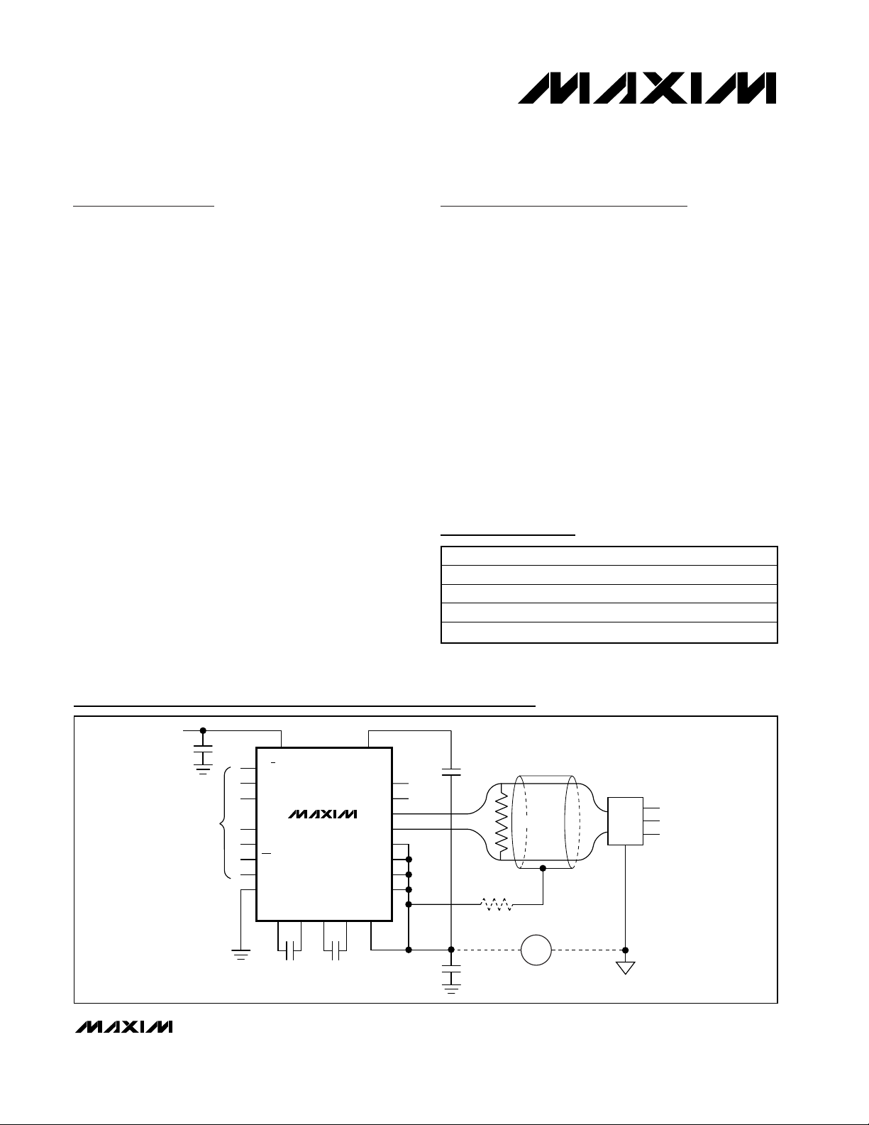
The MAX3158 is a high CMRR RS-485/RS-422 data-communications interface providing ±60V isolation in a
hybrid microcircuit. A single +5V supply on the logic side
powers both sides of the interface, with external 100V
capacitors transferring power from the logic side to the
isolated side. Each MAX3158 contains one transmitter
and one receiver and is guaranteed to operate at data
rates up to 250kbps. Drivers are short-circuit current limited and protected against excessive power dissipation
by thermal shutdown circuitry that places the driver outputs into a high-impedance state. The receiver input has
a fail-safe feature that guarantees a logic-high receiver
output if the inputs are open, shorted, or connected to a
terminated transmission line with all drivers disabled.
The MAX3158 typically draws 25mA of supply current
when unloaded or when fully loaded with the driver disabled. Supply current drops to 25µA when the device is
placed in shutdown mode. The device is pin selectable
between half- and full-duplex mode and also features
an independently programmable receiver and transmitter output phase through separate pins. The MAX3158
is a low-cost replacement for opto-isolated transceivers. For fully isolated RS-485/RS-422 transceivers,
refer to the MAX1480 family data sheet.
________________________Applications
Industrial Controls Telecommunications
Level Translators Local Area Networks
Features
♦ ±60V Isolated Data Interface
♦ +5V Single Supply
♦ Low-Cost Replacement for Opto-Isolated
Transceivers
♦ True Fail-Safe Receiver While Maintaining
EIA/TIA-485 Compliance
♦ Pin-Selectable Full/Half-Duplex Operation
♦ Phase Controls to Correct for Twisted-Pair
Reversal
♦ 25µA Low-Power Shutdown Mode
♦ Thermal Shutdown for Driver Overload Protection
♦ 28-Pin SSOP Package
♦ Slew-Rate-Limited Reduced EMI
MAX3158
High CMRR RS-485 Transceiver
with ±60V Isolation
________________________________________________________________ Maxim Integrated Products 1
Typical Operating Circuit
19-2778; Rev 0; 2/03
Ordering Information
Pin Configurations appear at end of data sheet.
PART TEMP RANGE
PIN-PACKAGE
MAX3158CAI 0°C to +70°C 28 SSOP
MAX3158CPI 0°C to +70°C 28 PDIP
MAX3158EAI -40°C to +85°C 28 SSOP
MAX3158EPI -40°C to +85°C 28 PDIP
For pricing, delivery, and ordering information, please contact Maxim/Dallas Direct! at
1-888-629-4642, or visit Maxim’s website at www.maxim-ic.com.
V
CC
0.1µF
MICRO
V
CC
H/F
TXP
RXP
DE
MAX3158
DI
RE
RO
GND
C1HI C2LO C2HIC1LO
C1
0.047µFC20.047µF
ISOVCC
A
B
Y
Z
YR
ZR
AR
BR
ISOCOM
C3
1µF
RS-485
NODE
REMOTE GND
10nF
RT = 100Ω
RG
±60V
C4
GND OFFSET
REMOTE MICRO
MAX3158
High CMRR RS-485 Transceiver
with ±60V Isolation
2 _______________________________________________________________________________________
ABSOLUTE MAXIMUM RATINGS
(All voltages referenced to GND, unless otherwise noted.)
ELECTRICAL CHARACTERISTICS
(VCC= +5V ±5%, YR = ZR = AR = BR = ISOCOM, C1 = C2 = 0.047µF, C3 = C4 = 1µF, TA= T
MIN
to T
MAX
, unless otherwise noted.
Typical values are at V
CC
= +5V and TA= +25°C.) (Note 1)
Stresses beyond those listed under “Absolute Maximum Ratings” may cause permanent damage to the device. These are stress ratings only, and functional
operation of the device at these or any other conditions beyond those indicated in the operational sections of the specifications is not implied. Exposure to
absolute maximum rating conditions for extended periods may affect device reliability.
Supply Voltage (VCC).............................................................+7V
Cable Ground (ISOCOM) ....................................................±75V
Isolated Supply ISOVCC Relative to Cable Ground
(ISOCOM) ...........................................................................+7V
Digital Input, Output Voltage
(DI, DE, RE, TXP, RXP, RO).....................-0.3V to (V
CC
+ 0.3V)
Digital Inputs (H/F) Relative to Cable Ground
(ISOCOM) .........................................-0.3V to (ISOVCC + 0.3V)
Driver Output Voltage (Y, Z) Relative to Cable Ground
(ISOCOM)............................................................-8V to +12.5V
Receiver Input Voltage (A, B) Relative to Cable Ground
(ISOCOM)............................................................-8V to +12.5V
Termination Connections (YR, ZR, AR, BR) Relative to Cable
Ground (ISOCOM)...............................................-8V to +12.5V
Charge-Pump Capacitance Low
(C1LO, C2LO) .........................................-0.3V to (V
CC
+ 0.3V)
Charge-Pump Capacitance High (C1HI, C2HI) Relative
to Cable Ground (ISOCOM) .............-0.3V to (ISOVCC + 0.3V)
Continuous Power Dissipation (T
A
= +70°C)
28-Pin SSOP (derate 10.8mW/°C above +70°C) ..........860mW
28-Pin PDIP (derate 14.3mW/°C above +70°C)..........1143mW
Operating Temperature Ranges
MAX3158C_I .......................................................0°C to +70°C
MAX3158E_I ....................................................-40°C to +85°C
Junction Temperature......................................................+150°C
Storage Temperature Range ............................-65°C to +160°C
Lead Temperature (soldering, 10s) ................................+300°C
DRIVER
Differential Driver Output,
No Load
Differential Driver Output,
Loaded
Change in Magnitude of
Differential Output Voltage
(Note 2)
PARAMETER SYMBOL CONDITIONS MIN TYP MAX UNITS
V
V
∆V
OD1
OD2
Figure 1, R = 10MΩ 6V
Figure 1, R = 50Ω (RS-422) 2.0
Figure 1, R = 27Ω (RS-485) 1.5
Figure 1, R = 50Ω or R = 27Ω 0.2 V
OD
V
Driver Common-Mode Voltage V
Change in Magnitude of
Common-Mode Voltage
(Note 2)
Input High Voltage V
Input Low Voltage V
DI Input Hysteresis V
OC
∆V
HYS
Figure 1, R = 50Ω or R = 27Ω,
relative to ISOCOM
V
OC
Figure 1, R = 50Ω or R = 27Ω 0.2 V
OC
DE, DI, RE, TXP, RXP, relative to GND,
IH
H/F relative to ISOCOM
DE, DI, RE, TXP, RXP, relative to GND,
IL
H/F relative to ISOCOM
2.0 V
100 mV
3.5 V
0.8 V
MAX3158
High CMRR RS-485 Transceiver
with ±60V Isolation
_______________________________________________________________________________________ 3
ELECTRICAL CHARACTERISTICS (continued)
(VCC= +5V ±5%, YR = ZR = AR = BR = ISOCOM, C1 = C2 = 0.047µF, C3 = C4 = 1µF, TA= T
MIN
to T
MAX
, unless otherwise noted.
Typical values are at V
CC
= +5V and TA= +25°C.) (Note 1)
PARAMETER SYMBOL CONDITIONS MIN TYP MAX UNITS
Input Current
Input Current (A and B) I
Output Leakage (Y and Z)
Full Duplex
Driver Short-Circuit Output
Current (Note 3)
RECEIVER
Receiver Differential Threshold
Voltage
Receiver Input Hysteresis ∆V
Receiver Output High Voltage V
Receiver Output Low Voltage V
Three-State Output Current at
Receiver
Receiver Input Resistance R
Receiver Output Short-Circuit
Current
SUPPLY CURRENT
Supply Current I
Supply Current in Shutdown
Mode
Maximum Ground Differential ∆V
I
I
IN1
IN2
DE, DI, RE ±2
H/F, TXP, RXP internal pulldown 10 40
DE = GND, VCC = GND or 5.25V, -7V ≤ (VIN V
IN3
DE = GND, VCC = GND or 5.25V, -7V ≤ (VIN V
DE = GND, VCC = GND or 5.25V, -7V ≤ (VIN -
I
V
O
DE = GND, VCC = GND or 5.25V, -7V ≤ (VIN V
I
OSD1
I
OSD2
V
OH
I
OZR
V
V
-7V ≤ VCM - V
TH
TH
IO = -4mA, VID = -50mV V CC - 1.5 V
IO = 4mA, VID = -200mV 0.4
OL
0.4V ≤ VO ≤ 2.4V ±1µA
-7V ≤ VCM - V
ISOCOM
IN
-7V ≤ VCM - V
BR open
I
OSR
CC
I
SHDN
GND
0V ≤ VRO ≤ V
No load, RE = DE = DI = GND or V
DE = GND, RE = VCC, V
DE = GND, RE = VCC, V
DE = GND, RE = VCC,
| ISOCOM leakage | ≤ 650µA
) ≤ +12V, AR = BR = ISOCOM
ISOCOM
) ≤ +12V, AR open, BR open
ISOCOM
) ≤ +12V, YR = ZR = ISOCOM
ISOCOM
) ≤ +12V, YR open, ZR open
ISOCOM
ISOCOM
ISOCOM
- 7V ≤ V
- 7V ≤ V
CC
≤ V
OUT
≤ V
OUT
≤ +12V -200 -125 -50 m V
ISOCOM
≤ +12V, AR = BR =
ISOCOM
≤ +12V, AR open,
ISOCOM
ISOVCC
+ 12V 250
ISOCOM
CC
= GND 25 60
ISOCOM
ISOCOM
= ±60V ±650
-5.0 +8.0
-0.58 +1.0
-5.0 +8.0
-0.58 +1.0
-250
25 mV
1.5
12
±7 ±100 mA
25 85 mA
±60 V
µA
mA
mA
mA
V
kΩ
µA
MAX3158
High CMRR RS-485 Transceiver
with ±60V Isolation
4 _______________________________________________________________________________________
SWITCHING CHARACTERISTICS
(VCC= +5V ±5%, YR = ZR = AR = BR = ISOCOM, C1 = C2 = 0.047µF, C3 = C4 = 1µF. Typical values are at VCC= +5V and TA= +25°C.)
Note 1: All currents into the device are positive; all currents out of the device are negative. All voltages are referred to device
ground unless otherwise noted.
Note 2: ∆V
OD
and ∆VOCare the changes in VODand VOC, respectively, when the DI input changes state.
Note 3: Current level applies to peak current just prior to foldback-current limiting.
Note 4: The device is put into shutdown by bringing RE high and DE low. If the enable inputs are in this state for less than 50ns,
the device is guaranteed not to enter shutdown. If the enable inputs are in this state for at least 700ns, the device is guaranteed to have entered shutdown.
Driver Input to Output
Driver Output Skew
| t
Driver Rise or Fall Time tDR, t
Maximum Data Rate f
Driver Enable to Output High t
Driver Enable to Output Low t
Driver Disable Time from Low t
Driver Disable Time from High t
Receiver Input to Output
Differential Receiver Skew
| t
Receiver Enable to Output Low t
Receiver Enable to Output High t
Receiver Disable Time from Low t
Receiver Disable Time from High t
Time to Shutdown t
Driver Enable from Shutdown to
Output High
Driver Enable from Shutdown to
Output Low
Receiver Enable from Shutdown
to Output High
Receiver Enable from Shutdown
to Output Low
Charge-Pump Oscillating
Frequency
PARAMETER SYMBOL CONDITIONS MIN TYP MAX UNITS
DPLH
RPLH
- t
- t
DPHL
RPHL
t
DPLH
t
DPHL
t
|
|
DSKEW
MAX
DZH
DZL
DLZ
DHZ
t
RPLH
t
RPHL
t
RSKEW
RZL
RZH
RLZ
RHZ
SHDN
t
DZH
(SHDN)
t
DZL
(SHDN)
t
RZH
(SHDN)
t
RZL
(SHDN)
f
OSC
Figures 3 and 5, R
C
= CL2 = 100pF
L1
Figures 3 and 5, R
C
= CL2 = 100pF
L1
Figures 3 and 5, R
C
= CL2 = 100pF
L1
Figures 3 and 5, R
DF
C
= CL2 =100pF
L1
Figures 4 and 6, CL = 100pF, S2 closed 3500 ns
Figures 4 and 6, CL = 100pF, S1 closed 3500 ns
Figures 4 and 6, CL = 15pF, S1 closed 300 ns
Figures 4 and 6, CL = 15pF, S2 closed 300 ns
,
Figures 7 and 9; | VID | ≥ 2.0V 440 600 ns
Figures 7 and 9; | VID | ≥ 2.0V 20 ns
Figures 2 and 8, CL = 100pF, S1 closed 20 50 ns
Figures 2 and 8, CL = 100pF, S2 closed 20 50 ns
Figures 2 and 8, C
Figures 2 and 8, C
(Note 4) 50 200 700 ns
Figures 4 and 6, C
Figures 4 and 6, C
Figures 2 and 8, C
Figures 2 and 8, C
= 54Ω,
DIFF
DIFF
DIFF
DIFF
= 54Ω,
= 54Ω,
= 54Ω,
400 1400 2000
400 1400 2000
200 1200 2200 ns
250 kbps
= 100pF, S1 closed 200 500 ns
L
= 100pF, S2 closed 200 500 ns
L
= 15pF, S2 closed 0.2 1 ms
L
= 15pF, S1 closed 0.2 1 ms
L
= 100pF, S2 closed 0.2 1 m s
L
= 100pF, S1 closed 0.2 1 ms
L
1.3 MHz
250 ns
ns
MAX3158
High CMRR RS-485 Transceiver
with ±60V Isolation
_______________________________________________________________________________________ 5
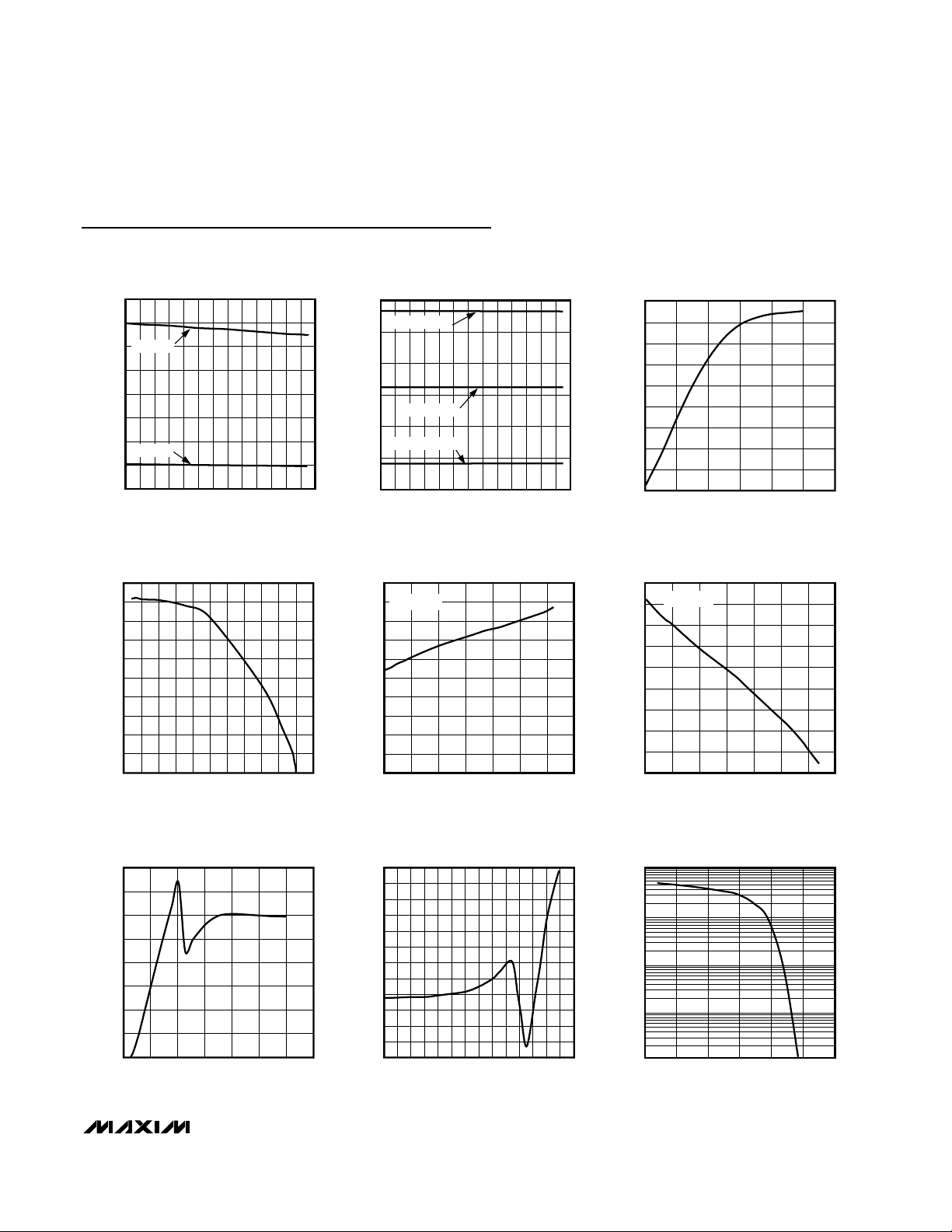
Typical Operating Characteristics
(VCC= +5V, YR = ZR = AR = BR = ISOCOM, C1 = C2 = 0.047µF, C3 = 1µF, C4 = 10nF, TA= +25°C, unless otherwise noted.)
SUPPLY CURRENT vs. TEMPERATURE
160
140
RL = 54Ω
120
100
80
60
SUPPY CURRENT (mA)
40
NO LOAD
20
0
-40 -20 -10 0 10 20 30-30 40 50 60 70 80 90
TEMPERATURE (°C)
MAX3158 toc01
-100
SUPPY CURRENT (µA)
-200
-300
RECEIVER OUTPUT CURRENT
vs. RECEIVER OUTPUT HIGH VOLTAGE
20
18
16
14
12
10
8
6
OUTPUT CURRENT (mA)
4
2
0
0 2.0 2.51.51.00.5 3.0 3.5 4.0 4.5 5.0 5.5
OUTPUT HIGH VOLTAGE (V)
MAX3158 toc04
OUTPUT LOW VOLTAGE (V)
SHUTDOWN SUPPLY CURRENT
vs. TEMPERATURE
300
V
= -50V
ISOCOM
200
100
0
V
= 0V
ISOCOM
V
= +50V
ISOCOM
-40 -20 -10 0 10 20 30-30 40 50 60 70 80 90
TEMPERATURE (°C)
RECEIVER OUTPUT LOW VOLTAGE
vs. TEMPERATURE
0.50
IRO = 8mA
0.45
0.40
0.35
0.30
0.25
0.20
0.15
0.10
0.05
0
-40 -20 0 20 40 60 80 100
TEMPERATURE (°C)
MAX3158 toc02
OUTPUT CURRENT (mA)
4.40
4.35
MAX3158 toc05
4.30
4.25
4.20
4.15
4.10
OUTPUT VOLTAGE (V)
4.05
4.00
3.95
RECEIVER OUTPUT CURRENT
vs. RECEIVER OUTPUT LOW VOLTAGE
45
40
35
30
25
20
15
10
5
0
021 3456
OUTPUT LOW VOLTAGE (V)
RECEIVER OUTPUT HIGH VOLTAGE
vs. TEMPERATURE
IRO = -8mA
-40 -20 0 20 40 60 80 100
TEMPERATURE (°C)
MAX3158 toc03
MAX3158 toc06
DRIVER OUTPUT CURRENT
vs. DRIVER OUTPUT LOW VOLTAGE
160
140
120
100
80
60
OUTPUT CURRENT (mA)
40
20
0
042 6 8 101214
OUTPUT VOLTAGE (V)
0
-10
-20
MAX3158 toc07
-30
-40
-50
-60
-70
-80
OUTPUT CURRENT (mA)
-90
-100
-110
-120
DRIVER OUTPUT CURRENT
vs. DRIVER OUTPUT HIGH VOLTAGE
MAX3158 toc08
-8 -4-6 -20246
OUTPUT HIGH VOLTAGE (V)
DRIVER OUTPUT CURRENT
vs. DIFFERENTIAL OUTPUT VOLTAGE
100
10
1
OUTPUT CURRENT (mA)
0.1
0.01
01 32546
DIFFERENTIAL OUTPUT VOLTAGE (V)
MAX3158 toc09

MAX3158
High CMRR RS-485 Transceiver
with ±60V Isolation
6 _______________________________________________________________________________________
Typical Operating Characteristics (continued)
(VCC= +5V, YR = ZR = AR = BR = ISOCOM, C1 = C2 = 0.047µF, C3 = 1µF, C4 = 10nF, TA= +25°C, unless otherwise noted.)
DRIVER DIFFERENTIAL OUTPUT
VOLTAGE vs. TEMPERATURE
1.98
RL = 54Ω
1.96
1.94
1.92
1.90
1.88
1.86
OUTPUT VOLTAGE (V)
1.84
1.82
1.80
-40 0-20 20 40 60 80
TEMPERATURE (°C)
MAX3158 toc10
PROPAGATION DELAY (ns)
RECEIVER PROPAGATION DELAY
vs. TEMPERATURE
490
480
470
460
450
440
430
420
410
-40 0-20 20 40 60 80
TEMPERATURE (°C)
MAX3158 toc11
DRIVER PROPAGATION DELAY
vs. TEMPERATURE
1.52
RL = 54Ω
1.50
1.48
1.46
1.44
1.42
1.40
1.38
PROPAGATION DELAY (µs)
1.36
1.34
1.32
-40 0-20 20 40 60 80
TEMPERATURE (°C)
MAX3158 toc12
DRIVER ENABLE TIME
vs. TEMPERATURE
1.500
1.475
1.450
1.425
1.400
1.375
DRIVER ENABLE TIME (µs)
1.350
1.325
1.300
-40 0-20 20 40 60 80 100
TEMPERATURE (°C)
DRIVER PROPAGATION DELAY
0V
0V
MAX3158 toc16
250
MAX3158 toc13
200
150
100
DRIVER DISABLE TIME (ns)
50
DI
2V/div
VY - VZ
DRIVER DISABLE TIME
vs. TEMPERATURE
0
-40 0-20 20 40 60 80 100
TEMPERATURE (°C)
POWER-UP DELAY
= 0V)
(V
ISOCOM
MAX3158 toc17
MAX3158 toc14
DE
10V/div
VY
5V/div
RECEIVER PROPAGATION DELAY
0V
0V
POWER-UP DELAY
(V
ISOCOM
0V
-50V
2µs/div
= -50V)
MAX3158 toc15
MAX3158 toc18
V
- V
A
5V/div
R
O
DE
5V/div
VY
10V/div
B
R
= 54Ω
DIFF
CL1 = CL2 = 100pF
2µs/div
40µs/div
100µs/div

MAX3158
High CMRR RS-485 Transceiver
with ±60V Isolation
_______________________________________________________________________________________ 7
Test Circuits and Timing Diagrams
Figure 1. Driver DC Test Load
Figure 3. Driver Timing Test Circuit
Figure 2. Receiver Enable/Disable Timing Test Load
Figure 4. Driver Enable/Disable Timing Test Load
Typical Operating Characteristics (continued)
(VCC= +5V, YR = ZR = AR = BR = ISOCOM, C1 = C2 = 0.047µF, C3 = 1µF, C4 = 10nF, TA= +25°C, unless otherwise noted.)
+50V
POWER-UP DELAY
= +50V)
(V
ISOCOM
0V
100µs/div
MAX3158 toc19
DE
5V/div
VY
10V/div
MAXIMUM COMMON-MODE VOLTAGE TO
GROUND vs. COMMON-MODE FREQUENCY
70
MAXIMUM COMMON-MODE
VOLTAGE TO ISOCOM
60
50
40
30
20
10
COMMON-MODE VOLTAGE TO GROUND (V)
0
0.1 1 10
COMMON-MODE VOLTAGE TO
ISOCOM = 7V PEAK
COMMON-MODE FREQUENCY (kHz)
MAX3158 toc20
Y
R
V
OD
R
V
OC
3V
DE
DI
Y
V
ID
Z
C
L1
R
DIFF
C
L2
Z
RECEIVER
OUTPUT
TEST POINT
C
100pF
L
1kΩ
1kΩ
S1
S2
V
CC
OUTPUT
UNDER TEST
500Ω
C
L
S1
S2
V
CC

MAX3158
High CMRR RS-485 Transceiver
with ±60V Isolation
8 _______________________________________________________________________________________
Figure 5. Driver Propagation Delays
Figure 6. Driver Enable and Disable Times
Figure 7. Receiver Propagation Delays
Figure 8. Receiver Enable and Disable Times
Figure 9. Receiver Propagation Delay Test Circuit
Test Circuits and Timing Diagrams (continued)
3V
DI
V
DIFF
1.5V
0V
Z
V
O
Y
1/2 V
O
V
O
0V
-V
10%
O
t
DR
90%
3V
DE
Y, Z
V
Y, Z
1.5V 1.5V
0V
t
DZL(SHDN)
OL
0V
2.3V
2.3V
t
DZH(SHDN)
t
DPLH
V
DIFF
t
DSKEW = | tDPLH
OUTPUT NORMALLY LOW
OUTPUT NORMALLY HIGH
t
= V (Y) - V (Z)
- t
, t
DZL
, t
DZH
DPHL
DPHL
t
DLZ
t
DHZ
t
1.5V
1/2 V
O
90%
DF
|
10%
3V
RE
0V
V
CC
RO
RO
0V
1.5V 1.5V
t
, t
RZL(SHDN)
1.5V
OUTPUT NORMALLY LOW
OUTPUT NORMALLY HIGH
1.5V
t
, t
RZH(SHDN)
RZL
RZH
t
RLZ
t
RHZ
V
V
OL
OH
+ 0.5V
- 0.5V
V
V
OL
OH
+ 0.5V
- 0.5V
ATE
B
V
ID
R
R
A
RECEIVER
OUTPUT
V
OH
-1V
RO
V
OL
A
1V
B
1.5V 1.5V
t
t
RSKEW = | tRPLH
RPHL
INPUT
OUTPUT
- t
RPHL
t
RPLH
|

MAX3158
High CMRR RS-485 Transceiver
with ±60V Isolation
_______________________________________________________________________________________ 9
Pin Description
PIN
SSOP
PDIP
NAME FUNCTION
12 RO
Receiver Output. When RE is low and A - B > -50mV, RO will be high; if A - B ≤ -200mV,
RO will be low.
23 RE Receiver Output Enable. Drive RE low to enable RO.
3 4 DE Driver Output Enable. Drive DE high to enable driver outputs.
45 DI
Driver Input. With DE high, a low on DI forces the noninverting output low and the inverting
output high; with DI high, outputs reverse.
5 6 C1LO Connect to the negative terminal of C1 (0.047µF, 100V).
6, 7,
12, 22,
23
1, 12,
14, 15,
28
N.C. No Connection. Not internally connected.
8 7 C1HI Connect to the positive terminal of C1 (0.047µF, 100V).
9 8 ISOVCC
Internally generated power-supply voltage, referenced to the cable ground (ISOCOM).
Connect a 1µF capacitor to ISOCOM.
10 9 H/F
Half/Full-Duplex Selector Pin. Leave open, or connect to ISOCOM to select Full Duplex,
or connect to ISOVCC to select Half Duplex.
11 10 ZR
Connect to ISOCOM for a 1.5kΩ input impedance on Z. Leave open for a 12kΩ input
impedance on Z.
13 11 YR
Connect to ISOCOM for a 1.5kΩ input impedance on Y. Leave open for a 12kΩ input
impedance on Y.
14 13
Cable Ground
15 16 Z Inverting Driver Output (and Inverting Receiver Input in Half-Duplex Mode)
16 17 Y Noninverting Driver Output (and Noninverting Receiver Input in Half-Duplex Mode)
17 18 B Inverting Receiver Input in Full-Duplex Mode
18 19 A Noninverting Receiver Input in Full-Duplex Mode
19 20 BR
Connect to ISOCOM for a 1.5kΩ input impedance on B. Leave open for a 12kΩ input
impedance on B.
20 21 AR
Connect to ISOCOM for a 1.5kΩ input impedance on A. Leave open for a 12kΩ input
impedance on A.
21 22 C2HI Connect to the positive terminal of C2 (0.047µF, 100V).
24 23 C2LO Connect to the negative terminal of C2 (0.047µF, 100V).
25 24 GND Ground
26 25 TXP
Transmitter Phase. Leave open, or connect to GND for normal transmitter polarity, or connect
to V
CC
to invert the transmitter polarity.
27 26 RXP
Receiver Phase. Leave open, or connect to GND for normal receiver polarity, or connect to
V
CC
to invert the receiver polarity.
28 27 V
CC
+4.75V to +5.25V Positive Supply. Connect a 0.1µF capacitor to GND.
ISOCOM

MAX3158
High CMRR RS-485 Transceiver
with ±60V Isolation
10 ______________________________________________________________________________________
Detailed Description
The MAX3158 is a high CMRR RS-485/RS-422 datacommunications interface providing ±60V isolation in a
hybrid microcircuit. A single +5V supply on the logic
side powers both sides of the interface, with external
100V capacitors transferring power from the logic side
to the isolated side (see Block Diagram). The MAX3158
typically draws 25mA of supply current when unloaded
or when fully loaded with the driver disabled. Supply
current drops to 25µA when the device is placed in
shutdown mode (see Low-Power Shutdown Mode section). The MAX3158 transceiver for RS-485/RS-422
communication contains one driver and one receiver.
This device features fail-safe circuitry, which guarantees a logic-high receiver output when the receiver
inputs are open or shorted, or when they are connected
to a terminated transmission line with all drivers disabled (see Fail-Safe section). The MAX3158 is selectable between half- and full-duplex communication by
connecting a selector pin to ISOVCC or ISOCOM,
respectively. Drivers are output short-circuit current limited. Thermal shutdown circuitry protects drivers
against excessive power dissipation. When activated,
the thermal shutdown circuitry places the driver outputs
into a high-impedance state. The device also features
independently programmable receiver and transmitter
output phase through separate pins. The MAX3158 is a
low-cost replacement for opto-isolated transceivers.
Fail-Safe
The MAX3158 guarantees a logic-high receiver output
when the receiver inputs are shorted or open, or when
they are connected to a terminated transmission line with
all drivers disabled. The receiver threshold is fixed
between -50mV and -200mV. If the differential receiver
input voltage (A - B) is greater than or equal to -50mV,
RO is logic high. If A - B is less than or equal to -200mV,
RO is logic low. In the case of a terminated bus with all
transmitters disabled, the receiver’s differential input voltage is pulled to 0V by the termination. With the receiver
thresholds of the MAX3158, this results in a logic high
with a 50mV minimum noise margin. Unlike competitor’s
fail-safe devices, the -50mV to -200mV threshold complies with the ±200mV EIA/TIA-485 standard.
MAX3158 Programming
The MAX3158 has several programmable operating
modes. Occasionally, twisted-pair lines are reversed.
The MAX3158 has two pins that invert the phase of the
driver and the receiver to correct for this problem. For
normal operation, drive TXP and RXP low, connect
them to ground, or leave them unconnected (internal
pulldown). To invert the driver phase, drive TXP high or
connect it to VCC. To invert the receiver phase, drive
RXP high or connect it to VCC. Note that the receiver
threshold is positive when RXP is high.
The MAX3158 can operate in full- or half-duplex mode.
Connect H/F to ISOCOM for full-duplex mode, and connect it to ISOVCC for half-duplex operation. In halfduplex mode, the receiver inputs are switched to the
driver outputs, connecting outputs Y and Z to inputs A
and B, respectively. In half-duplex mode, the internal
full-duplex receiver input resistors are still connected to
pins A and B.
Low-Power Shutdown Mode
The low-power shutdown mode is initiated by bringing
both RE high and DE low. In shutdown, this device typi-
cally draws only 25µA of supply current, and no power
is transferred across the isolation capacitors in this
mode. RE and DE may be driven simultaneously; the
parts are guaranteed not to enter shutdown if RE is
high and DE is low for less than 50ns. If the inputs are
in this state for at least 700ns, the parts are guaranteed
to enter shutdown. Enable times t_ZHand t_ZLin the
Switching Characteristics table assume the part was
not in a low-power shutdown state. Enable times
t_
ZH
(SHDN)
and t_
ZL
(SHDN)
assume the parts were shut
down. It takes drivers and receivers longer to become
enabled from low-power shutdown mode t_
ZH
(SHDN)
,
t_
ZL
(SHDN)
than from driver/receiver-disable mode
(t_ZH, t_ZL).
Driver Output Protection
Two mechanisms prevent excessive output current and
power dissipation caused by faults or by bus contention. The first, a foldback current limit on the output
stage, provides immediate protection against short circuits over the whole common-mode voltage range (see
Typical Operating Characteristics). The second, a thermal shutdown circuit, forces the driver outputs into a
high-impedance state if the die temperature becomes
excessive—typically around +150°C.
Applications Information
Capacitor and Grounding Resistor
Selection
The value for the charge-pump capacitors C1 and C2
should be between 47nF and 100nF. Smaller values will
result in insufficient supply voltage on the isolated side.
Larger values are allowed but will not result in better
charge-pump capacity. The values for C1 and C2, as
well as that of C4, determine the maximum frequency
and amplitude of the voltage difference (under operating conditions) between the local and isolated ground.
Besides the capacitor values, this maximum frequency

MAX3158
High CMRR RS-485 Transceiver
with ±60V Isolation
______________________________________________________________________________________ 11
and amplitude are also determined by the resistance
between the remote ground and the ISOCOM pin. The
receiver input resistors will cause the isolated common
voltage to go to the mean voltage of the receiver inputs,
which will be a direct function of the remote ground
potential. The receiver input resistance and the capacitors C1, C2, and C4 set up a time constant that limits
how fast the ISOCOM pin can follow variations in the
remote ground voltage. Connecting YR and ZR in halfduplex operation, or AR and BR in full-duplex operation,
to ISOCOM results in a relatively low input impedance of
the MAX3158 receiver inputs (2kΩ). This allows for a
60Hz sine wave with a 60V maximum amplitude (see
Typical Operating Characteristics). If YR, ZR, AR, and
BR are left open, the receiver input impedance is 12kΩ
allowing up to 32 transceivers on the bus. To guarantee
the same low time constant under those conditions, use
a shielded cable with a 1kΩ resistor connected between
the shield and ISOCOM. Using a lower value for this
resistor is not recommended because this could trigger
a holding current in the internal ESD protection device if
the ±75V isolation limit is exceeded.
A single point hard-ground connection for the shield is
recommended.
Communication Between
Two MAX3158s
If two MAX3158 devices are used to communicate with
each other, one of the devices must have ISOCOM
connected to local ground. Failure to do so will result in
floating ISOCOM pins, with both devices trying to adapt
to the isolated ground of the other.
Chip Information
TRANSISTOR COUNT: 1309
Block Diagram
TXP
RXP
V
DI
DE
RO
RE
MAX3158
CC
OSC
POWER
Y
Z
YR
ZR
A
B
AR
BR
H/F
H/F
ISOVCC
GND C1L C2L C1H C2H ISOCOM

MAX3158
High CMRR RS-485 Transceiver
with ±60V Isolation
12 ______________________________________________________________________________________
Pin Configurations
TOP VIEW
RO
RE
DE
DI
C1LO
N.C.
N.C.
C1HI
ISOVCC
H/F
ZR
N.C.
YR
ISOCOM
1
2
3
4
5
6
7
8
9
10
11
12
13
14
MAX3158
28 SSOP
28
V
CC
27
RXP
26
TXP
25
GND
24
C2LO
23
N.C.
22
N.C.
21
C2HI
20
AR
19
BR
18
A
17
B
16
Y
15
Z
N.C.
C1LO
C1HI
ISOVCC
H/F
N.C.
ISOCOM
N.C.
1
2
RO
3
RE
4
DE
5
DI
ZR
YR
MAX3157MAX3158
6
7
8
9
10
11
12
13
14
28
N.C.
V
27
CC
RXP
26
25
TXP
GND
24
C2LO
23
C2HI
22
AR
21
BR
20
A
19
B
18
Y
17
Z
16
N.C.
15
28 PDIP

MAX3158
High CMRR RS-485 Transceiver
with ±60V Isolation
______________________________________________________________________________________ 13
Package Information
(The package drawing(s) in this data sheet may not reflect the most current specifications. For the latest package outline information,
go to www.maxim-ic.com/packages
.)
e
D
12
MAX
0.078
0.008
0.015
0.008
0.212
0.311
0.037
8∞
MILLIMETERS
MAX
MIN
1.73 1.99
0.05
0.21
0.25
0.38
0.09
0.20
5.20
5.38
0.65 BSC
7.90
7.65
0.63
0.95
0∞
8∞
MAX
0.249
0.249
0.289
0.328
0.407
MILLIMETERS
MAX
MIN
6.07
6.33
6.07
6.33
7.07
7.33
8.07
8.33
10.07
10.33
N
14L
16L
20L
24L
28L
C
INCHES
MIN
D
0.239
D
0.239
D
0.278
D
0.317
0.397
D
INCHES
DIM
MIN
A
0.068
A1
0.002
B
0.010
C
HE
N
A
B
A1
D
E
e
H
L
0.004
SEE VARIATIONS
0.205
0.0256 BSC
0.301
0.025
0∞
L
SSOP.EPS
NOTES:
1. D&E DO NOT INCLUDE MOLD FLASH.
2. MOLD FLASH OR PROTRUSIONS NOT TO EXCEED .15 MM (.006").
3. CONTROLLING DIMENSION: MILLIMETERS.
4. MEETS JEDEC MO150.
5. LEADS TO BE COPLANAR WITHIN 0.10 MM.
PROPRIETARY INFORMATION
TITLE:
PACKAGE OUTLINE, SSOP, 5.3 MM
21-0056
REV.DOCUMENT CONTROL NO.APPROVAL
1
C
1

Maxim cannot assume responsibility for use of any circuitry other than circuitry entirely embodied in a Maxim product. No circuit patent licenses are
implied. Maxim reserves the right to change the circuitry and specifications without notice at any time.
14 ____________________Maxim Integrated Products, 120 San Gabriel Drive, Sunnyvale, CA 94086 408-737-7600
© 2003 Maxim Integrated Products Printed USA is a registered trademark of Maxim Integrated Products.
MAX3158
High CMRR RS-485 Transceiver
with ±60V Isolation
Package Information (continued)
(The package drawing(s) in this data sheet may not reflect the most current specifications. For the latest package outline information,
go to www.maxim-ic.com/packages
.)
PDIPN.EPS
 Loading...