

For free samples & the latest literature: http://www.maxim-ic.com, or phone 1-800-998-8800.
For small orders, phone 1-800-835-8769.
General Description
The MAX3140 is a complete universal asynchronous
receiver-transmitter (UART) and a true fail-safe RS485/RS-422 transceiver combined in a single 28-pin
QSOP package for space-, cost-, and power-constrained applications. The MAX3140 saves additional
board space as well as microcontroller (µC) I/O pins by
featuring an SPI™/QSPI™/MICROWIRE™-compatible
serial interface. It is pin-programmable for configuration
in all RS-485/RS-422 networks.
The MAX3140 includes a single RS-485/RS-422 driver
and receiver featuring true fail-safe circuitry, which
guarantees a logic-high receiver output when the
receiver inputs are open or shorted. This feature provides immunity to faults without requiring complex termination. The MAX3140 provides software-selectable
control of half- or full-duplex operation, data rate, slew
rate, and transmitter and receiver phase. The RS-485
driver slew rate is programmable to minimize EMI and
results in maximum data rates of 115kbps, 500kbps,
and 10Mbps. Independent transmitter/receiver phase
control enables software correction of twisted-pair
polarity reversal. A 1/8-unit-load receiver input impedance allows up to 256 transceivers on the bus.
The MAX3140’s UART includes an oscillator circuit
derived from an external crystal, and a baud-rate generator with software-programmable divider ratios for all
common baud rates from 300 baud to 230k baud. The
UART features an 8-word-deep receive FIFO that minimizes processor overhead and provides a flexible interrupt with four maskable sources, including address
recognition on 9-bit networks. Two control lines are
included for hardware handshaking—one input and
one output.
The MAX3140 operates from a single +5V supply and
typically consumes only 645µA with the receiver active.
Hardware-invoked shutdown reduces supply current to
only 20µA. The UART and RS-485/RS-422 functions can
be used together or independently since the two functions share only supply and ground connections (the
MAX3140 is hardware- and software-compatible with the
MAX3100 and MAX3089).
Applications
Industrial-Control Transceivers for EMILocal Area Networks Sensitive Applications
HVAC and Building Control Embedded Systems
Point-of-Sale Devices Intelligent Instrumentation
Features
♦ Integrated UART and RS-485/RS-422 Transceiver
in a Single 28-Pin QSOP
♦ SPI/MICROWIRE-Compatible Interface Saves µC
I/O Pins
♦ True Fail-Safe Receiver Output Eliminates
Complex Network Termination
♦ Pin-Programmable RS-485/RS-422 Features
Half/Full-Duplex Operation
Slew-Rate Limiting for Reduced EMI
115kbps/500kbps/10Mbps Data Rates
Receiver/Transmitter Phase for Twisted-Pair
Polarity Reversal
♦ Full-Featured UART
Programmable Up to 230k baud with a
3.6864MHz Crystal
8-Word Receive FIFO Minimizes Processor
Overhead
9-Bit Address-Recognition Interrupt
♦ Allows Up to 256 Transceivers on the Bus
♦ Low 20µA Hardware Shutdown Mode
♦ Hardware/Software-Compatible with MAX3100
and MAX3089
MAX3140
SPI/MICROWIRE-Compatible UART with Integrated
True Fail-Safe RS-485/RS-422 Transceivers
________________________________________________________________
Maxim Integrated Products
1
19-1453; Rev 0; 6/99
PART
MAX3140CEI
MAX3140EEI -40°C to +85°C
0°C to +70°C
TEMP. RANGE PIN-PACKAGE
28 QSOP
28 QSOP
Ordering Information
SPI/QSPI are trademarks of Motorola, Inc.
MICROWIRE is a trademark of National Semiconductor Corp.
Pin Configuration appears at end of data sheet.
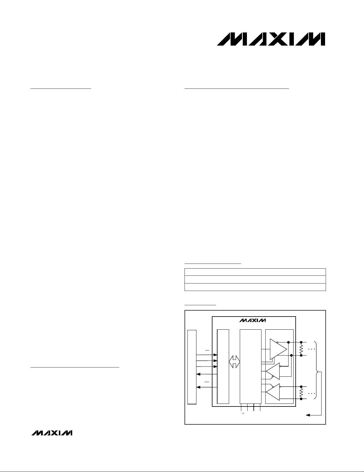
Typical Application Circuit
CS
SCLK
SPI/
MICRO-
WIRE
DIN
DOUT
µP
UART
IRQ
H/FSRL
R
t
HALF/FULL-DUPLEX
RS-485/RS-422
R
t
TXP
CONTROL
LOGIC
RS-485
RS-422
RXP
MAX3140
MAX3140
SPI/MICROWIRE-Compatible UART with Integrated
True Fail-Safe RS-485/RS-422 Transceivers
2 _______________________________________________________________________________________
ABSOLUTE MAXIMUM RATINGS
ELECTRICAL CHARACTERISTICS
(VCC= +5V ±5%, DE = VCC, RE = GND, SHDN = VCC, f
XTL
= 1.8432MHz, TA= T
MIN
to T
MAX
, unless otherwise noted. Typical values
are measured with V
CC
= +5V, UART configured for 9600 baud, TA= +25°C.) (Note 1)
Stresses beyond those listed under “Absolute Maximum Ratings” may cause permanent damage to the device. These are stress ratings only, and functional
operation of the device at these or any other conditions beyond those indicated in the operational sections of the specifications is not implied. Exposure to
absolute maximum rating conditions for extended periods may affect device reliability.
VCCto GND ..........................................................................+6V
Input Voltage to GND (CS, SHDN, X1, CTS, RX, DIN, SCLK,
RE, DE, H/F, SRL, TXP, RXP, Dl).............-0.3V to (V
CC
+ 0.3V)
Output Voltage to GND
DOUT, RTS, TX, X2, RO...........................-0.3V to (V
CC
+ 0.3V)
IRQ ........................................................................-0.3V to +6V
Driver Output Voltage (Y, Z) ...............................................±13V
Receiver Input Voltage, Half Duplex (Y, Z)......................... ±13V
Receiver Input Voltage, Full Duplex (A, B) .........................±25V
TX, RTS Output Current ...................................................100mA
X2, DOUT, IRQ Short-Circuit Duration
(to V
CC
or GND)......................................................Continuous
Continuous Power Dissipation (T
A
= +70°C)
28-pin QSOP (derate 10.8mW/°C above +70°C)..........860mW
Operating Temperature Ranges
MAX3140CEI .......................................................0°C to +70°C
MAX3140EEI ....................................................-40°C to +85°C
Storage Temperature Range.............................-65°C to +150°C
Lead Temperature (soldering, 10sec).............................+300°C
I
SOURCE
= 5mA; DOUT, RTS
SHDN = GND or SHDNi bit = 1;
DE = GND; RE = V
CC
SHDN = GND or SHDNi bit = 1
CONDITIONS
VCC- 0.5
pF5C
IN2
Input Capacitance
µA±1I
LKG1
Input Leakage Current
mV250V
HYST2
Input Hysteresis
V0.3V
CC
V
IL2
Input Low Voltage
V0.7V
CC
V
IH2
Input High Voltage
pF5C
IN1
Input Capacitance
25
V0.2V
CC
V
IL1
Input Low Voltage
V0.7V
CC
V
IH1
Input High Voltage
0.64 1.6
0.7 1.9
µA20
I
CC
SHDN
(FULL)
Supply Current with Both
RS-485 Transceiver and UART
Shut Down
0.74 2
mA
0.69 1.8
I
CC
Supply Current
mA0.47 1
I
CC
SHDN
UART
Supply Current with Only UART
Shut Down
UNITSMIN TYP MAXSYMBOLPARAMETER
I
SINK
= 4mA; DOUT, RTS
I
SOURCE
= 10mA; TX only
0.4
V
VCC- 0.5
V
OH1
Output High Voltage
V4.75 5.25V
CC
Supply Voltage
VX1= 0 or V
CC
µA
2
I
IN1
Input Current
SHDNi bit = 0
SHDNi bit = 1
I
SINK
= 25mA; TX only
V
0.9
V
OL1
Output Low Voltage
CS = VCC; D
OUT
only
µA
5
I
LKG2
Output Leakage ±1
C
OUT1
Output Capacitance pF
SHDN = VCC;
SHDNi bit = 0,
no load
DE = V
CC
DE = GND
DE = V
CC
DE = GND
SRL = V
CC
SRL = GND
or open
UART OUTPUTS (DOUT, TX, RTS)
UART LOGIC INPUTS (DIN, SCLK, CS, SHDN, CTS, RX)
UART OSCILLATOR INPUT (X1)
POWER SUPPLY
MAX3140
SPI/MICROWIRE-Compatible UART with Integrated
True Fail-Safe RS-485/RS-422 Transceivers
_______________________________________________________________________________________ 3
ELECTRICAL CHARACTERISTICS (continued)
(VCC= +5V ±5%, DE = VCC, RE = GND, SHDN = VCC, f
XTL
= 1.8432MHz, TA= T
MIN
to T
MAX
, unless otherwise noted. Typical values
are measured with V
CC
= +5V, UART configured for 9600 baud, TA= +25°C.) (Note 1)
R = 50Ω or R = 27Ω, Figure 1
R = 50Ω or R = 27Ω, Figure 1 (Note 2)
R = 27Ω (RS-422), Figure 1
R = 50Ω (RS-422), Figure 1
No load, Figure 1
V
IRQ
= V
CC
I
SINK
= 4mA
R = 50Ω or R = 27Ω, Figure 1 (Note 2)
CONDITIONS
V3V
OC
Common-Mode Output
Voltage
V0.2∆V
OD
Change in Magnitude of
Differential Output Voltage
V
1.5
V
OD2
Differential Output Voltage 2.0
5V
OD1
pF5C
OUT2
Output Capacitance
µA±1I
LKG3
Output Leakage
V0.4V
OL2
Output Low Voltage
V0.2∆V
OC
Change In Magnitude of
Common-Mode Voltage
UNITSMIN TYP MAXSYMBOLPARAMETER
(Note 3)
H/F, TXP, RXP, internal pull-down
DE, DI, RE
SRL = VCCor unconnected
DE, Dl, RE, H/F, TXP, RXP
DE, Dl, RE
SRL = GND (Note 3)
SRL = V
CC
V
0.4 · V
CC
0.6 · V
CC
V
IM2
SRL Input Middle Voltage
VVCC- 0.8V
IH2
SRL Input High Voltage
µA
10 40I
IN2
Input Current
±2I
IN1
mV100V
HYS
DI Input Hysteresis
V0.8V
IL1
Input Low Voltage
2.0
µA
-75
I
IN3
SRL Input Current
75
V0.8V
IL2
SRL Input Low Voltage
(Note 4)
DE = GND
VCC= GND or 5.25V
DE = GND
250
-250
µA
125
I
O
Full-Duplex Output Leakage
(Y and Z)
µA
-75
I
IN4
125
Full-Duplex Input Current
(A and B)
mA
±25
I
OSD
Short-Circuit Output Current
-7V ≤ VCM≤ +12V mV-200 -125 -50V
TH
mV25∆V
TH
Input Hysteresis
Differential Threshold Voltage
I
SINK
= 4mA, VID= -200mV
I
SOURCE
= 4mA, VID= -50mV
0.4V ≤ VO≤ 2.4V
V0.4V
OL
VVCC- 1.5V
OH
µA±1I
OZR
Output High Voltage
Three-State Output Current
Output Low Voltage
-7V ≤ VCM≤ 12V
0 ≤ VRO≤ V
CC
kΩ96R
IN
mA±7 ±95I
OSR
Output Short-Circuit Current
Input Resistance
VIN= 12V
VIN= -7V
VCC= GND or 5.25V
VIN= 12V
VIN= -7V -100
-7V ≤ V
OUT
≤ V
CC
0 ≤ V
OUT
≤ 12V
0 ≤ V
OUT
≤ V
CC
H/F, TXP, RXP
V
2.4
V
IH1
Input High Voltage
UART IRQ OUTPUT (Open Drain)
RS-485 DRIVER
RS-485 RECEIVER

MAX3140
SPI/MICROWIRE-Compatible UART with Integrated
True Fail-Safe RS-485/RS-422 Transceivers
4 _______________________________________________________________________________________
UART SWITCHING CHARACTERISTICS
(VCC= +5V ±5%, f
XTL
= 1.8432MHz, TA= T
MIN
to T
MAX
, unless otherwise noted. Typical values are measured with VCC= +5V,
UART configured for 9600 baud, T
A
= +25°C.) (Note 1)
CONDITIONS UNITSMIN TYP MAXSYMBOLPARAMETER
C
LOAD
= 100pF ns100t
DV
CS Low to DOUT Valid
C
LOAD
= 100pF, RCS= 10kΩ ns100t
TR
CS High to DOUT Tri-State
ns0t
CSH
CS to SCLK Hold Time
ns100t
CSS
CS to SCLK Setup Time
ns100t
DS
DIN to SCLK Setup Time
ns238t
CP
SCLK Period
ns0t
DH
DIN to SCLK Hold Time
C
LOAD
= 100pF ns100t
DO
SCLK Fall to DOUT Valid
ns100t
CL
SCLK Low Time
ns200t
CS1
CS Rising Edge to SCLK
Rising
ns100t
CS0
SCLK Rising Edge to CS
FaIling
TX, RTS, DOUT; C
LOAD
= 100pF
ns10t
r
Output Rise Time
TX, RTS, DOUT, IRQ; C
LOAD
= 100pF
ns10t
f
Output Fall Time
ns200t
CSW
CS High Pulse Width
ns100t
CH
SCLK High Time
UART AC TIMING (Figure 1)

MAX3140
SPI/MICROWIRE-Compatible UART with Integrated
True Fail-Safe RS-485/RS-422 Transceivers
_______________________________________________________________________________________ 5
SWITCHING CHARACTERISTICS—SRL = Unconnected
(VCC= +5V ±5%, TA= T
MIN
to T
MAX
, unless otherwise noted. Typical values are at VCC= +5V and TA= +25°C.)
500 2030 2600t
DPHL
PARAMETER SYMBOL MIN TYP MAX UNITS
Driver Disable Time from Low t
DLZ
100 ns
Driver Enable to Output Low t
DZL
3500 ns
Driver Enable to Output High t
DZH
3500 ns
Maximum Data Rate f
MAX
115 kbps
Driver Disable Time from High t
DHZ
100 ns
Receiver Input to Output
t
RPLH
,
t
RPHL
127 200 ns
|
t
RPLH
- t
RPHL
|
Differential
Receiver Skew
t
RSKD
3±30ns
Receiver Enable to Output Low t
RZL
20 50 ns
Driver Output Skew
|
t
DPLH
- t
DPHL
|
Driver Input to Output
t
DPLH
500 2030 2600
ns
t
DSKEW
-3 ±200 ns
Driver Rise or Fall Time tDR, t
DF
667 1320 2500 ns
Receiver Enable to Output High t
RZH
20 50 ns
Receiver Disable Time from Low t
RLZ
20 50 ns
Receiver Disable Time from
High
t
RHZ
20 50 ns
Time to Shutdown t
SHDN
50 200 600 ns
Driver Enable from Shutdown to
Output High
t
DZH(SHDN)
6000 ns
Driver Enable from Shutdown to
Output Low
t
DZL(SHDN)
6000 ns
Receiver Enable from Shutdown
to Output High
t
RZH(SHDN)
3500 ns
Receiver Enable from Shutdown
to Output Low
t
RZL(SHDN)
3500 ns
CONDITIONS
Figures 2 and 8, CL= 100pF, S2 closed
Figures 4 and 6, CL= 15pF, S1 closed
Figures 2 and 8, CL= 100pF, S1 closed
Figures 4 and 6, CL= 100pF, S1 closed
Figures 4 and 6, CL= 100pF, S2 closed
Figures 4 and 6, CL= 15pF, S2 closed
Figures 7 and 9, |V
ID
|
≥ 2.0V,
rise and fall time of V
ID
≤ 15ns
Figures 2 and 8, CL= 100pF, S2 closed
(Note 5)
Figures 7 and 9, |V
ID
|
≥ 2.0V,
rise and fall time of V
ID
≤ 15ns
Figures 2 and 8, CL= 100pF, S1 closed
Figures 4 and 6, CL= 15pF, S2 closed
Figures 4 and 6, CL= 15pF, S1 closed
Figures 2 and 8, CL= 100pF, S2 closed
Figures 3 and 5, R
DIFF
= 54Ω,
CL1= CL2= 100pF
Figures 2 and 8, CL= 100pF, S1 closed
Figures 3 and 5, R
DIFF
= 54Ω,
CL1= CL2= 100pF
Figures 3 and 5, R
DIFF
= 54Ω,
CL1= CL2= 100pF

MAX3140
SPI/MICROWIRE-Compatible UART with Integrated
True Fail-Safe RS-485/RS-422 Transceivers
6 _______________________________________________________________________________________
SWITCHING CHARACTERISTICS—SRL = V
CC
(VCC= +5V ±5%, TA= T
MIN
to T
MAX
, unless otherwise noted. Typical values are at VCC= +5V and TA= +25°C.)
250 720 1000
Receiver Enable from Shutdown
to Output Low
t
RZL(SHDN)
3500 nsFigures 2 and 8, CL= 100pF, S1 closed
t
DPHL
PARAMETER SYMBOL MIN TYP MAX UNITS
Driver Disable Time from Low t
DLZ
100 ns
Driver Enable to Output Low t
DZL
2500 ns
Driver Enable to Output High t
DZH
2500 ns
Maximum Data Rate f
MAX
500 kbps
Driver Disable Time from High t
DHZ
100 ns
Receiver Input to Output
t
RPLH
,
t
RPHL
127 200 ns
|
t
RPLH
- t
RPHL
|
Differential
Receiver Skew
t
RSKD
3±30ns
Receiver Enable to Output Low t
RZL
20 50 ns
Driver Output Skew
|
t
DPLH
- t
DPHL
|
Driver Input to Output
t
DPLH
250 720 1000
ns
t
DSKEW
-3 ±100 ns
Driver Rise or Fall Time t
DR, tDF
200 530 750 ns
Receiver Enable to Output High t
RZH
20 50 ns
Receiver Disable Time from Low t
RLZ
20 50 ns
Receiver Disable Time from
High
t
RHZ
20 50 ns
Time to Shutdown t
SHDN
50 200 600 ns
Driver Enable from Shutdown to
Output High
t
DZH(SHDN)
4500 ns
Driver Enable from Shutdown to
Output Low
t
DZL(SHDN)
4500 ns
Receiver Enable from Shutdown
to Output High
t
RZH(SHDN)
3500 ns
CONDITIONS
Figures 2 and 8, CL= 100pF, S2 closed
Figures 4 and 6, CL= 15pF, S1 closed
Figures 2 and 8, CL= 100pF, S1 closed
Figures 4 and 6, CL= 100pF, S1 closed
Figures 4 and 6, CL= 100pF, S2 closed
Figures 4 and 6, CL= 15pF, S2 closed
Figures 7 and 9, |V
ID
|
≥ 2.0V,
rise and fall time of V
ID
≤ 15ns
Figures 2 and 8, CL= 100pF, S2 closed
(Note 5)
Figures 7 and 9, |V
ID
|
≥ 2.0V,
rise and fall time of V
ID
≤ 15ns
Figures 2 and 8, CL= 100pF, S1 closed
Figures 4 and 6, CL= 15pF, S2 closed
Figures 4 and 6, CL= 15pF, S1 closed
Figures 2 and 8, CL= 100pF, S2 closed
Figures 3 and 5, R
DIFF
= 54Ω,
CL1= CL2= 100pF
Figures 3 and 5, R
DIFF
= 54Ω,
C
L1
= CL2= 100pF
Figures 3 and 5, R
DIFF
= 54Ω,
CL1= CL2= 100pF

MAX3140
SPI/MICROWIRE-Compatible UART with Integrated
True Fail-Safe RS-485/RS-422 Transceivers
_______________________________________________________________________________________ 7
SWITCHING CHARACTERISTICS—SRL = GND
(VCC= +5V ±5%, TA= T
MIN
to T
MAX
, unless otherwise noted. Typical values are at VCC= +5V and TA= +25°C.)
PARAMETER SYMBOL MIN TYP MAX UNITS
Driver Disable Time from Low t
DLZ
100 ns
Driver Enable to Output Low t
DZL
150 ns
Driver Enable to Output High t
DZH
150 ns
Maximum Data Rate f
MAX
10 Mbps
Driver Disable Time from High t
DHZ
100 ns
Receiver Input to Output
t
RPLH
,
t
RPHL
106 150 ns
|
t
RPLH
- t
RPHL
|
Differential
Receiver Skew
t
RSKD
0±10ns
Receiver Enable to Output Low t
RZL
20 50 ns
Driver Output Skew
|
t
DPLH
- t
DPHL
|
Driver Input to Output
t
DPLH
34 60
ns
t
DSKEW
-2.5 ±10 ns
Driver Rise or Fall Time t
DR, tDF
14 25 ns
Receiver Enable to Output High t
RZH
20 50 ns
Receiver Disable Time from Low t
RLZ
20 50 ns
Receiver Disable Time from
High
t
RHZ
20 50 ns
Time to Shutdown t
SHDN
50 200 600 ns
Driver Enable from Shutdown to
Output High
t
DZH(SHDN)
250 ns
Driver Enable from Shutdown to
Output Low
t
DZL(SHDN)
250 ns
Receiver Enable from Shutdown
to Output High
t
RZH(SHDN)
3500 ns
34 60
CONDITIONS
Figures 2 and 8, CL= 100pF, S2 closed
Figures 4 and 6, CL= 15pF, S1 closed
Figures 2 and 8, CL= 100pF, S1 closed
Figures 4 and 6, CL= 100pF, S1 closed
Figures 4 and 6, CL= 100pF, S2 closed
Figures 4 and 6, CL= 15pF, S2 closed
Figures 7 and 9, |V
ID
|
≥ 2.0V,
rise and fall time of V
ID
≤ 15ns
Figures 2 and 8, CL= 100pF, S2 closed
(Note 5)
Figures 7 and 9, |V
ID
|
≥ 2.0V,
rise and fall time of V
ID
≤ 15ns
Figures 2 and 8, CL= 100pF, S1 closed
Figures 4 and 6, CL= 15pF, S2 closed
Figures 4 and 6, CL= 15pF, S1 closed
Figures 2 and 8, CL= 100pF, S2 closed
Figures 3 and 5, R
DIFF
= 54Ω,
CL1= CL2= 100pF
Receiver Enable from Shutdown
to Output Low
Figures 3 and 5, R
DIFF
= 54Ω,
CL1= CL2= 100pF
t
RZL(SHDN)
3500
Figures 3 and 5, R
DIFF
= 54Ω,
CL1= CL2= 100pF
nsFigures 2 and 8, CL= 100pF, S1 closed
t
DPHL
Note 1: All currents into the device are positive; all currents out of the device are negative. All voltages are referred to device
ground unless otherwise noted.
Note 2: ∆V
OD
and ∆VOCare the changes in VODand VOC, respectively, when the Dl input changes state.
Note 3: The SRL pin is internally biased to V
CC
/2 by a 100kΩ/100kΩ resistor-divider. It is guaranteed to be VCC/2 if left unconnected.
Note 4: Maximum current level applies to peak current just prior to foldback-current limiting; minimum current level applies during
current limiting.
Note 5: The device is put into shutdown by bringing RE high and DE low. If the enable inputs are in this state for less than 50ns, the
device is guaranteed not to enter shutdown. If the enable inputs are in this state for at least 600ns, the device is guaranteed
to have entered shutdown.
MAX3140
SPI/MICROWIRE-Compatible UART with Integrated
True Fail-Safe RS-485/RS-422 Transceivers
8 _______________________________________________________________________________________
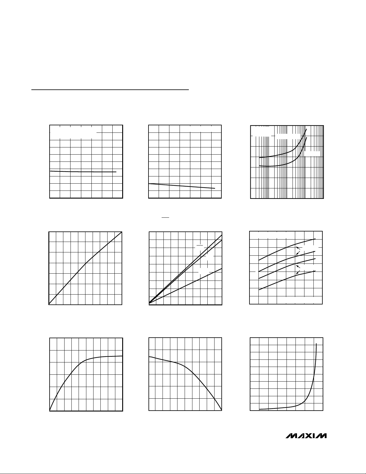
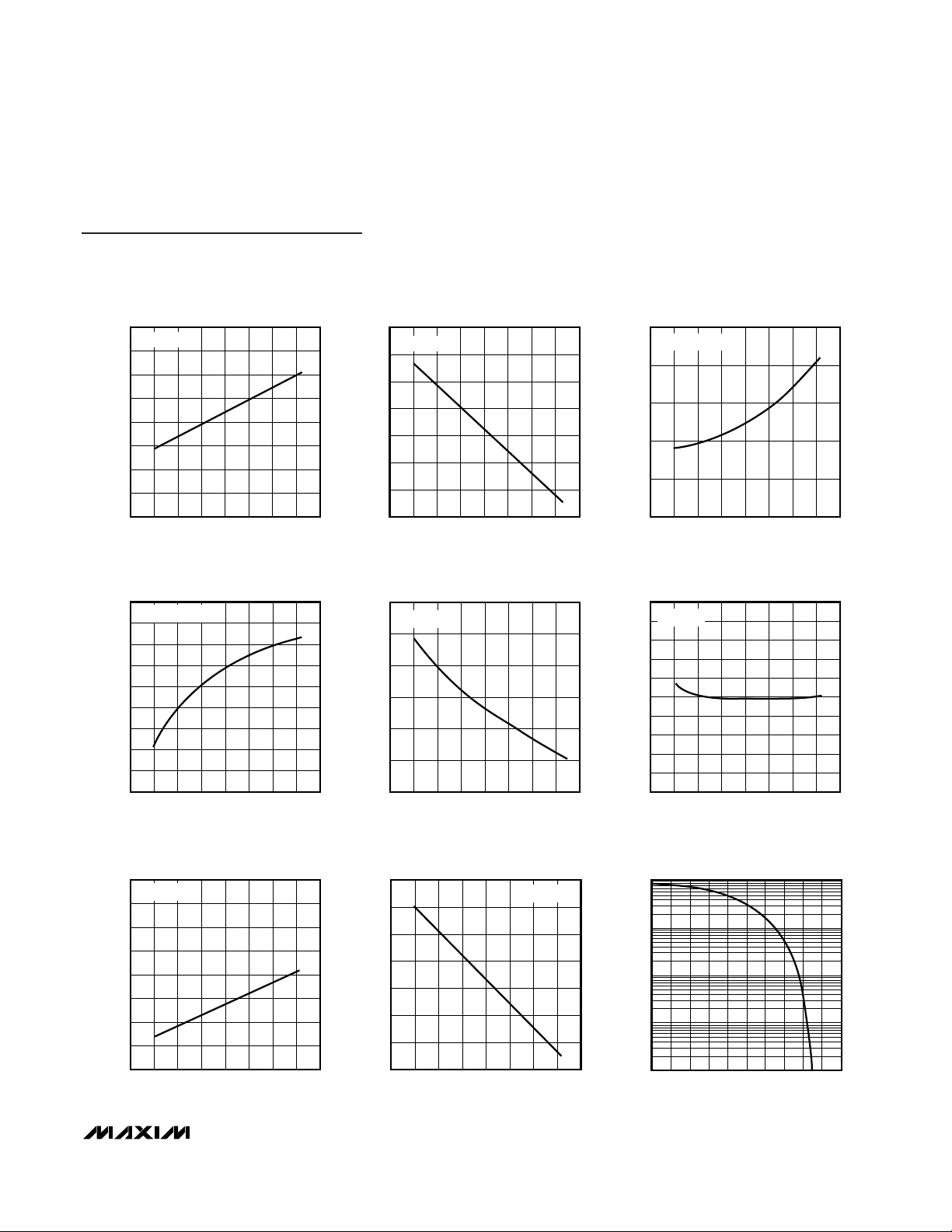
Typical Operating Characteristics
(VCC= +5V, TA = +25°C, unless otherwise noted.)
1000
900
0
-40 -20 40 60 100
UART SUPPLY CURRENT
vs. TEMPERATURE
200
100
800
700
MAX3140-01
TEMPERATURE (°C)
SUPPLY CURRENT (µA)
020 80
600
500
400
300
1.8432MHz CRYSTAL
TRANSMITTING AT 115.2 kbps
10
9
0
-40 -20 40 60 100
UART SHUTDOWN CURRENT
vs. TEMPERATURE
2
1
8
7
MAX3140-02
TEMPERATURE (°C)
SHUTDOWN CURRENT (µA)
020 80
6
5
4
3
1.8432MHz CRYSTAL
400
50
100 10k
1000
100k 1M
UART SUPPLY CURRENT
vs. BAUD RATE
150
100
MAX3140-03
BAUD RATE (bps)
SUPPLY CURRENT (µA)
200
250
350
300
TRANSMITTING
1.8432 MHz
CRYSTAL
STANDBY
700
600
0
01 3
4
5
UART SUPPLY CURRENT vs.
EXTERNAL CLOCK FREQUENCY
100
500
MAX3140-04
EXTERNAL CLOCK FREQUENCY (MHz)
SUPPLY CURRENT (µA)
2
400
300
200
0
10
05
RS-485 OUTPUT CURRENT
vs. RECEIVER OUTPUT LOW VOLTAGE
20
60
MAX3140-07
OUTPUT LOW VOLTAGE (V)
OUTPUT CURRENT (mA)
3
40
30
2
50
14
90
80
0
0 0.20.1 0.6 0.7
0.8
1.0
TX, RTS, DOUT OUTPUT CURRENT
vs. OUTPUT LOW VOLTAGE
10
70
MAX3140-05
OUTPUT LOW VOLTAGE (V)
OUTPUT SINK CURRENT (mA)
0.3 0.50.4 0.9
60
50
40
30
20
RTS
TX
DOUT
300
-60 100
RS-485 TRANSCEIVER NO-LOAD
SUPPLY CURRENT vs. TEMPERATURE
350
325
525
MAX3140-06
TEMPERATURE (°C)
NO-LOAD SUPPLY CURRENT (µA)
40
450
425
375
400
060
500
475
-40 -20 20 80
A: SRL = GND
B: SRL = OPEN OR V
CC
A
A
B
DE = V
CC
DE = GND
B
0
5
05
RS-485 OUTPUT CURRENT
vs. RECEIVER OUTPUT HIGH VOLTAGE
10
30
MAX3140-08
OUTPUT HIGH VOLTAGE (V)
OUTPUT CURRENT (mA)
3
20
15
2
25
14
0
2
-60 100
RS-485 TRANSCEIVER SHUTDOWN
CURRENT vs. TEMPERATURE
4
6
20
MAX3140-09
TEMPERATURE (°C)
SHUTDOWN CURRENT (nA)
40
12
14
10
8
060
16
18
-40 -20 20 80
MAX3140
SPI/MICROWIRE-Compatible UART with Integrated
True Fail-Safe RS-485/RS-422 Transceivers
_______________________________________________________________________________________
9
0.10
0.15
-60 80 100
RS-485 RECEIVER OUTPUT LOW VOLTAGE
vs. TEMPERATURE
0.20
0.50
MAX3140-10
TEMPERATURE (°C)
OUTPUT LOW VOLTAGE (V)
20
0.40
0.35
0.30
0.25
040
0.45
-40 -20 60
IRO = 8mA
3.8
3.9
-60 80 100
RS-485 RECEIVER OUTPUT HIGH VOLTAGE
vs. TEMPERATURE
4.0
4.5
MAX3140-11
TEMPERATURE (°C)
OUTPUT HIGH VOLTAGE (V)
20
4.3
4.2
4.1
040
4.4
-40 -20 60
IRO = 8mA
115
-60 100
RS-485 RECEIVER PROPAGATION DELAY
(500kbps MODE) vs. TEMPERATURE
120
140
MAX3140-12
TEMPERATURE (°C)
PROPAGATION DELAY (ns)
40
130
125
060
135
-40 -20 20 80
C
LOAD
= 100pF
94
-60 100
RS-485 RECEIVER PROPAGATION DELAY
(10Mbps MODE) vs. TEMPERATURE
98
96
112
MAX3140-13
TEMPERATURE (°C)
PROPAGATION DELAY (ns)
40
106
104
100
102
060
110
108
-40 -20 20 80
C
LOAD
= 100pF
20
25
-60 100
RS-485 DRIVER PROPAGATION DELAY
(10Mbps MODE) vs. TEMPERATURE
30
60
MAX3140-16
TEMPERATURE (°C)
PROPAGATION DELAY (ns)
40
45
50
40
35
060
55
-40 -20 20 80
Rt = 54Ω
1.90
-60 100
RS-485 DRIVER PROPAGATION DELAY
(115kbps MODE) vs. TEMPERATURE
1.95
2.20
MAX3140-14
TEMPERATURE (°C)
PROPAGATION DELAY (µs)
40
2.10
2.00
2.05
060
2.15
-40 -20 20 80
Rt = 54Ω
520
560
-60 100
RS-485 DRIVER PROPAGATION DELAY
(500kbps MODE) vs. TEMPERATURE
600
640
920
MAX3140-15
TEMPERATURE (°C)
PROPAGATION DELAY (ns)
40
760
800
720
680
060
840
880
-40 -20 20 80
Rt = 54Ω
1.83
1.84
-60 100
RS-485 DRIVER DIFFERENTIAL
OUTPUT VOLTAGE vs. TEMPERATURE
1.85
1.90
MAX3140-17
TEMPERATURE (°C)
OUTPUT VOLTAGE (V)
40
1.88
1.87
1.86
060
1.89
-40 -20 20 80
Rt = 54Ω
100
0.01
01
RS-485 DRIVER OUTPUT CURRENT
vs. DIFFERENTIAL OUTPUT VOLTAGE
0.1
10
1
MAX3140-18
DIFFERENTIAL OUTPUT VOLTAGE (V)
OUTPUT CURRENT (mA)
2345
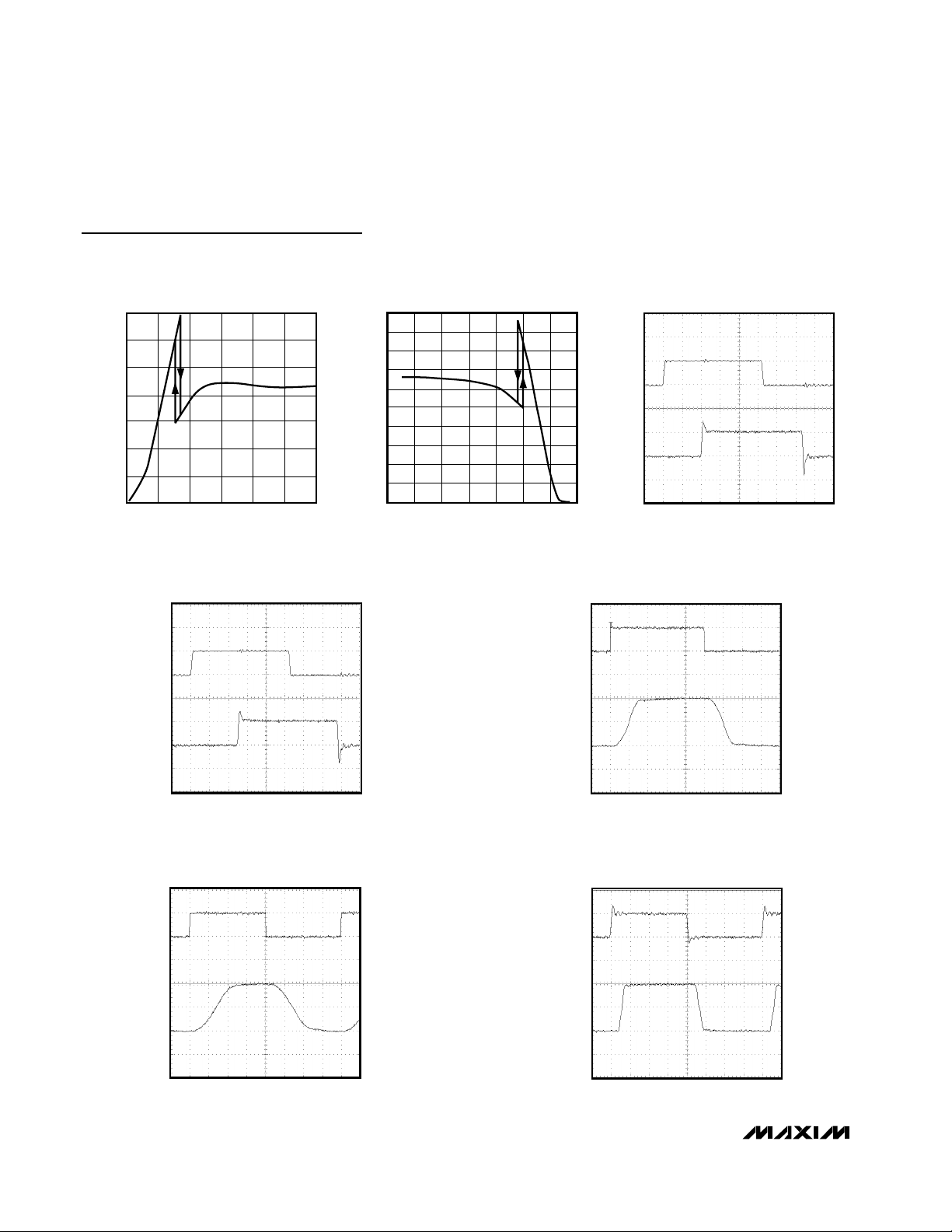
Typical Operating Characteristics (continued)
(VCC= +5V, TA = +25°C, unless otherwise noted.)
MAX3140
SPI/MICROWIRE-Compatible UART with Integrated
True Fail-Safe RS-485/RS-422 Transceivers
10 ______________________________________________________________________________________
Typical Operating Characteristics (continued)
(VCC= +5V, TA = +25°C, unless otherwise noted.)
0
20
40
60
80
100
120
140
OUTPUT CURRENT vs.
RS-485 DRIVER OUTPUT LOW VOLTAGE
MAX3140-19
OUTPUT LOW VOLTAGE (V)
OUTPUT CURRENT (mA)
024681012
0
-10
-20
-30
-40
-50
-60
-70
-80
-90
-100
-8 -2
OUTPUT CURRENT vs.
RS-485 DRIVER OUTPUT HIGH VOLTAGE
MAX3140-20
OUTPUT HIGH VOLTAGE (V)
OUTPUT CURRENT (mA)
642-6 -4 0
50ns/div
VA - V
B
(2V/div)
RO
(5V/div)
MAX3140-21
RS-485 RECEIVER PROPAGATION DELAY
(SRL = GND)
50ns/div
VA - V
B
(2V/div)
RO
(5V/div)
MAX3140-22
RS-485 RECEIVER PROPAGATION DELAY
(SRL = OPEN OR V
CC
)
2µs/div
RS-485 DRIVER PROPAGATION DELAY
(SRL = OPEN)
DI
(5V/div)
V
Y
- V
Z
(2.5V/div)
MAX3140-23
500ns/div
RS-485 DRIVER PROPAGATION DELAY
(SRL = V
CC
)
DI
(5V/div)
V
Y
- V
Z
(2.5V/div)
MAX3140-24
50ns/div
RS-485 DRIVER PROPAGATION DELAY
(SRL = GND)
DI
(5V/div)
V
Y
- V
Z
(2.5V/div)
MAX3140-25

MAX3140
SPI/MICROWIRE-Compatible UART with Integrated
True Fail-Safe RS-485/RS-422 Transceivers
______________________________________________________________________________________ 11
Pin Description
UART Crystal Connection. Leave X2 unconnected for external clock. See the
Crystals,
Oscillators, and Ceramic Resonators
section.
X21 1
2
UART Crystal Connection. X1 also serves as an external clock input. See the
Crystals,
Oscillators, and Ceramic Resonators
section.
X12
3
4
UART Request-to-Send Active-Low Output. Controlled by the RTS bit. Use to control the driver enable in RS-485 networks.
RTS
4
UART Clear-to-Send Active-Low Input. Read via the CTS bit.
CTS
3
5
6 UART Asynchronous Serial-Data (transmitter) OutputTX6
7
8 GroundGND8
RS-485 Half/Full-Duplex Selector Pin. Connect H/F to VCCfor half-duplex mode; connect H/F
to GND or leave it unconnected for full-duplex mode.
H/F
7
UART Asynchronous Serial-Data (receiver) Input. The serial information received from the modem
or RS-232/RS-485 receiver. A transition on RX while in shutdown generates an interrupt (Table 1).
RX5
9
10
RS-485 Receiver Output Enable. Drive RE low to enable RO; RO is high impedance when RE
is high. Drive RE high and DE low to enter low-power shutdown mode.
RE
10
11
12
RS-485 Driver Input. With DE high, a low on DI forces noninverting output low and inverting
output high. Similarly, a high on DI forces noninverting output high and inverting output low.
DI12
RS-485 Driver Output Enable. Drive DE high to enable driver outputs. These outputs are high
impedance when DE is low. Drive RE high and DE low to enter low-power shutdown mode.
DE11
13
14 No Connection. Not internally connected.N.C.14
15
— RS-485 Noninverting Driver OutputY16
RS-485 Transmitter Phase. Connect TXP to GND or leave it floating for normal transmitter
phase/polarity. Connect TXP to VCCto invert the transmitter phase/polarity.
TXP15
RS-485 Transceiver Slew-Rate-Limit Selector Pin. Connect SRL to GND for a 10Mbps communication rate, connect SRL to VCCfor a 500kbps rate, or leave SRL unconnected for a
115kbps rate.
SRL13
RS-485 Receiver Output. When RE is low and if A - B ≥ -50mV, RO will be high; if A - B ≤
-200mV, RO will be low.
RO9
16
17 No Connection. Not internally connected.N.C.17
—
18 RS-485 Inverting Receiver Input and RS-485 Inverting Driver Output*Z—
RS-485 Inverting Driver OutputZ18
—
19 RS-485 Receiver Input Resistors*B—
—
20 RS-485 Receiver Input Resistors*A—
RS-485 Noninverting Receiver InputA20
RS-485 Inverting Receiver InputB19
RS-485 Noninverting Receiver Input and RS-485 Noninverting Driver Output*Y—
FULL
DUPLEX
HALF
DUPLEX
PIN
NAME FUNCTION

MAX3140
SPI/MICROWIRE-Compatible UART with Integrated
True Fail-Safe RS-485/RS-422 Transceivers
12 ______________________________________________________________________________________
Pin Description (continued)
Transceiver Function Tables
21
22 Positive Supply (4.75V to 5.25V)V
CC
22
23
24
UART SPI/MICROWIRE Serial-Data Output. High impedance when CS is high.
DOUT24
UART SPI/MICROWIRE Serial-Data Input. Schmitt-trigger input.DIN23
25
26
UART Active-Low Chip-Select Input. DOUT goes high impedance when CS is high. IRQ, TX,
and RTS are always active. Schmitt-trigger input.
CS
26
27
28
UART Hardware Shutdown Input. When shut down (SHDN = 0), the UART oscillator turns off
immediately without waiting for the current transmission to end, reducing the supply current
to just leakage currents.
SHDN
28
UART Active-Low Interrupt Output. Open-drain interrupt output to microprocessor.
IRQ
27
UART SPI/MICROWIRE Serial-Clock Input. Schmitt-trigger input.SCLK25
RS-485 Receiver Phase. Connect RXP to GND or leave it unconnected for normal receiver
phase/polarity. Connect RXP to VCCto invert the receiver phase/polarity.
RXP21
FULL
DUPLEX
HALF
DUPLEX
PIN
NAME FUNCTION
*
In half-duplex mode, the driver outputs serve as receiver inputs. The full-duplex receiver inputs ( A and B) still have a 1/8-unit load, but
do not affect the receiver output.
RE
DETXP
TRANSMITTING
Z YDI
0 11X 10
1 00X 10
1 01X 11
0 10X 11
High-Z High-ZX0 0X
Shutdown (High-Z)X1 0X
0
0
0
0
1
1
H/F
OUTPUTSINPUTS
0
0
1
1
0
0
RXP
X
X
X
X
X
X
DE
0
0
0
0
0
0
RE
≥ -0.05V
≤ -0.2V
≥ -0.05V
≤ -0.2V
X
X
A-B
1
0
0
1
1
0
RO
X
X
X
X
≥ -0.05V
≤ -0.2V
Y-Z
1
1
0
0
1
1
X
X
X
X
X
X
1 0
0
0
1
0
0
0
0
X
X
Open/
Shorted
X1
Open/
Shorted
X
0
0
1
1
1
0
1 0
≥ -0.05V
≤ -0.2V
X
Open/
Shorted
X
Open/
Shorted
X
X
1
0
1
1
X
X
X High-Z
X
Shutdown
(High-Z)
X
X
OUTPUTS
RECEIVING
INPUTS

MAX3140
SPI/MICROWIRE-Compatible UART with Integrated
True Fail-Safe RS-485/RS-422 Transceivers
______________________________________________________________________________________ 13
R
R
Y
Z
V
OD
V
OC
Figure 1. Driver DC Test Load
RECEIVER
OUTPUT
TEST POINT
1k
1k
S1
S2
V
CC
C
L
15pF
Figure 2. Receiver Enable/Disable Timing Test Load
DI
DE
V
CC
Y
Z
C
L1
C
L2
R
DIFF
V
ID
Figure 3. Driver Timing Test Circuit
OUTPUT
UNDER TEST
500Ω
S1
S2
V
CC
C
L
Figure 4. Driver Enable/Disable Timing Test Load
DI
3V
0
Z
Y
V
O
0
-V
O
V
O
1.5V
t
PLH
1/2 V
O
10%
t
R
90%
90%
t
PHL
1.5V
1/2 V
O
10%
t
F
V
DIFF
= V (Y) - V (Z)
V
DIFF
t
SKEW = | tPLH
- t
PHL
|
Figure 5. Driver Propagation Delays
OUTPUT NORMALLY LOW
OUTPUT NORMALLY HIGH
3V
0
Y, Z
V
OL
Y, Z
0
1.5V 1.5V
V
OL
+0.5V
V
OH
-0.5V
2.3V
2.3V
t
ZL(SHDN)
, t
ZL
t
LZ
t
ZH(SHDN)
, t
ZH
t
HZ
DE
Figure 6. Driver Enable and Disable Times

MAX3140
SPI/MICROWIRE-Compatible UART with Integrated
True Fail-Safe RS-485/RS-422 Transceivers
14 ______________________________________________________________________________________
V
OH
V
OL
A
B
1V
-1V
1.5V 1.5V
OUTPUT
INPUT
RO
t
PLH
t
PHL
Figure 7. Receiver Propagation Delays
OUTPUT NORMALLY LOW
OUTPUT NORMALLY HIGH
3V
0
V
CC
RO
RO
0
1.5V 1.5V
V
OL
+ 0.5V
V
OH
- 0.5V
1.5V
1.5V
t
ZL(SHDN)
, t
ZL
t
LZ
t
ZH(SHDN)
, t
ZH
t
HZ
RE
Figure 8. Receiver Enable and Disable Times
R
B
RECEIVER
OUTPUT
ATE
A
V
ID
R
Figure 9. Receiver Propagation Delay Test Circuit
_______________Detailed Description
The MAX3140 combines an SPI/QSPI/MICROWIREcompatible UART (MAX3100) and an RS-485/RS-422
transceiver (MAX3089) in one package. The UART supports data rates up to 230k baud for both standard
UART bit streams as well as IrDA, and includes an
8-word receive FIFO. Also included is a parity-bit interrupt useful in 9-bit address recognition.
The RS-485/RS-422 transceiver has a true fail-safe
receiver and allows up to 256 transceivers on the bus.
Other features include pin-selectable full/half-duplex
operation and a phase control to correct for twisted-
pair reversal. The slew rate of the RS-485/RS-422 transceiver is selectable, limiting the maximum data rate to
115kbps, 500kbps, or 10Mbps. The RS-485/RS-422 drivers are output short-circuit current limited, and thermal
shutdown circuitry protects the RS-485/RS-422 drivers
against excessive power dissipation.
The UART and RS-485/RS422 functions can be used
together or independently since the two functions only
share supply and ground connections. This part operates from a single +5V supply.

UART
The universal asynchronous receiver transmitter
(UART) interfaces the SPI/MICROWIRE-compatible synchronous serial data from a microprocessor (µP) to
asynchronous, serial-data communication ports (RS485, IrDA). Figure 10 shows the MAX3140 functional
diagram. Included in the UART function is an
SPI/MICROWIRE interface, a baud-rate generator, and
an interrupt generator.
SPI Interface
The MAX3140 is compatible with SPI, QSPI (CPOL = 0,
CPHA = 0), and MICROWIRE serial-interface standards
(Figure 11). The MAX3140 has a unique full-duplex
architecture that expects a 16-bit word for DIN and
simultaneously produces a 16-bit word for DOUT
regardless of which read/write register used. The DIN
stream is monitored for its first two bits to tell the UART
the type of data transfer being executed (see the
WRITE CONFIGURATION register, READ CONFIGURATION register, WRITE DATA register,
and
READ
DATA register
sections). DIN (MOSI) is latched on
MAX3140
SPI/MICROWIRE-Compatible UART with Integrated
True Fail-Safe RS-485/RS-422 Transceivers
______________________________________________________________________________________ 15
RO
TXP
A
B
Y
Z
GND
DIN
CS
SCLK
DOUT
CTS
RTS
I/O
TX
IRQ
RX
X2
X1
9
9
4
9
9
99
P
t
P
t
P
r
P
r
P
r
SPI
INTERFACE
INTERRUPT
LOGIC
BAUD-RATE
GENERATOR
TX BUFFER
TX SHIFT REGISTSER
RX SHIFT REGISTSER
RX FIFO
RX BUFFER
DI
SRL
DE
H/F
RE
NOTE: SWITCH POSITIONS INDICATE H/F = GND
RXP
9
MAX3140
Figure 10. Functional Diagram
CS
SCLK
SCLK
SCLK
SCLK
(CPOL = 0, CPHA = 0)
(CPOL = 0, CPHA = 1)
(CPOL = 1, CPHA = 0)
(CPOL = 1, CPHA = 1)
COMPATIBLE
WITH MAX3140
NOT COMPATIBLE
WITH MAX3140
DIN
MSB 1314 12 11 10 9 8 7 6 5 4 3 2 1 LSB
DOUT
MSB 1314 12 11 10 9 8 7 6 5 4 3 2 1 LSB
Figure 11. Compatible CPOL and CPHA Modes

MAX3140
SCLK’s rising edge. DOUT (MISO) is read into the µP
on SCLK’s rising edge. The first bit (bit 15) of DOUT
transitions on CS’s falling edge, and bits 14–0 transition
on SCLK’s falling edge. Figure 12 shows the detailed
serial timing specifications for the synchronous SPI
port.
Only 16-bit words are expected. If CS goes high in the
middle of a transmission (any time before the 16th bit),
the sequence is aborted (i.e., data does not get written
to individual registers). Most operations, such as the
clearing of internal registers, are executed only on CS’s
rising edge. Every time CS goes low, a new 16-bit
stream is expected. Figure 13 shows an example of
using the WRITE CONFIGURATION register.
Table 1 describes the bits located in the WRITE CONFIGURATION, READ CONFIGURATION, WRITE DATA,
and READ DATA registers. This table also describes
whether the bit is a read or write bit and what the
power-on reset states (POR) of the bits are. Figure 14
shows an example of parity and word length control.
SPI/MICROWIRE-Compatible UART with Integrated
True Fail-Safe RS-485/RS-422 Transceivers
16 ______________________________________________________________________________________
• • •
• • •
• • •
• • •
CS
SCLK
DIN
DOUT
t
CSO
t
CL
t
DS
t
DH
t
DV
t
CH
t
DO
t
TR
t
CSH
t
CS1
t
CSS
Figure 12. Detailed Serial Timing Specifications for the Synchronous Port
1
CS
SCLK
DIN
DOUT
2 3 4 5 6 7 8 9 10 11 12 13 14 15 16
DATA
UPDATED
11 FEN SHDN TM RM PM RAM IR ST PE L B3 B2 B1 B0
RT 00 000 000000000
Figure 13. SPI Interface (Write Configuration)
IDLE
SECOND STOP BIT IS OMITTED IF ST = 0.
PE = 1, L = 1
TIME
D0START D1 D2 D3 D4 D5 D6 Pt
STOPSTOP
IDLE
IDLE
PE = 1, L = 0
D0START D1 D2 D3 D4 D5 D6 D7 Pt STOP STOP IDLE
IDLE
PE = 0, L = 1
D0START D1 D2 D3 D4 D5 D6 STOP STOP IDLE
IDLE
PE = 0, L = 0
D0START D1 D2 D3 D4 D5 D6 D7 STOP STOP IDLE
Figure 14. Parity and Word Length Control

MAX3140
SPI/MICROWIRE-Compatible UART with Integrated
True Fail-Safe RS-485/RS-422 Transceivers
______________________________________________________________________________________ 17
Table 1. Bit Descriptions
0PE
POR
STATE
write
Parity-Enable Bit. Appends the Pt bit to the transmitted data when PE = 1, and sends the Pt
bit as written. No parity bit is transmitted when PE = 0. With PE = 1, an extra bit is expected to
be received. This data is put into the Pr register. Pr = 0 when PE = 0. The MAX3140 does not
calculate parity.
0PE read Reads the value of the Parity-Enable bit.
0
PM
write
Mask for Pr bit. IRQ is asserted if PM = 1 and Pr = 1 (Table 7).
DESCRIPTION
0000
0000
XPr read
Receive-Parity Bit. This bit is the extra bit received if PE = 1. Therefore, PE = 1 results in 9-bit
transmissions (L = 0). If PE = 0, then Pr is set to 0. Pr is stored in the FIFO with the receive
data (see the
9-Bit Networks
section).
0
0
IR read Reads the value of the IR bit.
L
BIT
TYPE
write
B0–B3 write Baud-Rate Divisor Select Bits. Sets the baud clock’s value (Table 6).
B0–B3 read Baud-Rate Divisor Select Bits. Reads the 4-bit baud clock value assigned to these registers.
BIT
NAME
Bit to set the word length of the transmitted or received data. L = 0 results in 8-bit words
(9-bit words if PE = 1) (see Figure 5). L = 1 results in 7-bit words (8-bit words if PE = 1).
0
X
L read Reads the value of the L bit.
Pt write
Transmit-Parity Bit. This bit is treated as an extra bit that is transmitted if PE = 1. In 9-bit networks, the MAX3140 does not calculate parity. If PE = 0, then this bit (Pt) is ignored in transmit
mode (see the
9-Bit Networks
section).
00000000
0
D0r–D7r read
Eight data bits read from the receive FIFO or the receive-buffer register. When L = 1, D7r is
always 0.
FEN
write
FIFO Enable. Enables the receive FIFO when FEN = 0. When FEN = 1, FIFO is disabled.
0
0
FEN
read
FIFO-Enable Readback. FEN’s state is read.
IR write Enables the IrDA timing mode when IR = 1.
No
change
XXXXXXXX
CTS read
Clear-to-Send-Input. Records the state of the CTS pin (CTS bit = 0 implies CTS pin = logic
high).
D0t–D7t write
Transmit-Buffer Register. Eight data bits written into the transmit-buffer register. D7t is ignored
when L = 1.
0
PM
read
Reads the value of the PM bit (Table 7).
0R read
Receive Bit or FIFO Not Empty Flag. R = 1 means new data is available to be read or is being
read from the receive register or FIFO. If performing a READ DATA or WRITE DATA operation,
the R bit will clear on the falling edge of SCLK's 16th pulse if no new data is available.
0
RM
write
Mask for R bit. IRQ is asserted if RM = 1 and R = 1 (Table 7).
0
RM
read
Reads the value of the RM bit (Table 7).
0
RAM
write
Mask for RA/FE bit. IRQ is asserted if RAM = 1 and RA/FE = 1 (Table 7).
0
RAM
read
Reads the value of the RAM bit (Table 7).
0RTS write
Request-to-Send Bit. Controls the state of the RTS output. This bit is reset on power-up (RTS
bit = 0 sets the RTS pin = logic high).

MAX3140
SPI/MICROWIRE-Compatible UART with Integrated
True Fail-Safe RS-485/RS-422 Transceivers
18 ______________________________________________________________________________________
Table 1. Bit Descriptions (continued)
POR
STATE
DESCRIPTION
BIT
TYPE
BIT
NAME
0SHDNi write
Software-Shutdown Bit. Enter software shutdown with a WRITE CONFIGURATION where
SHDNi = 1. Software shutdown takes effect after CS goes high, and causes the oscillator to
stop as soon as the transmitter becomes idle. Software shutdown also clears R, T, RA/FE,
D0r–D7r, D0t–D7t, Pr, Pt, and all data in the receive FIFO. RTS and CTS can be read and
updated while in shutdown. Exit software shutdown with a WRITE CONFIGURATION where
SHDNi = 0. The oscillator restarts typically within 50ms of CS going high. RTS and CTS are
unaffected. Refer to the
Pin Description
for hardware shutdown (SHDN input).
0SHDNo read
Shutdown Read-Back Bit. The READ CONFIGURATION register outputs SHDNo = 1 when the
UART is in shutdown. Note that this bit is not sent until the current byte in the transmitter is
sent (T = 1). This tells the processor when it may shut down the RS-485/RS-422 driver. This bit
is also set immediately when the device is shut down through the SHDN pin.
0RA/FE read
Receiver-Activity/Framing-Error Bit. In shutdown mode, this is the RA bit. In normal operation,
this is the FE bit. In shutdown mode, a transition on RX sets RA = 1. In normal mode, a framing error sets FE = 1. A framing error occurs if a zero is received when the first stop bit is
expected. FE is set when a framing error occurs, and cleared upon receipt of the next properly framed character independent of the FIFO being enabled. When the device wakes up, it is
likely that a framing error will occur. This error is cleared with a WRITE CONFIGURATION. The
FE bit is not cleared on a READ DATA operation. When an FE is encountered, the UART
resets itself to the state where it is looking for a start bit.
0ST write
Transmit-Stop Bit. One stop bit will be transmitted when ST = 0. Two stop bits will be transmitted when ST = 1. The receiver only requires one stop bit.
0ST read Reads the value of the ST bit.
0
TM
write
Mask for T Bit. IRQ is asserted if TM = 1 and T = 1 (Table 7).
0
TM
read
Reads the value of the TM bit (Table 7).
1T read
Transmit-Buffer-Empty Flag. T = 1 means that the transmit buffer is empty and ready to
accept another data word.
0
TE
write
Transmit-Enable Bit. If TE = 1, then only the RTS pin is updated on CS’s rising edge. The contents of RTS, Pt, and D0t–D7t transmit on CS’s rising edge when TE = 0.
Notice to High-Level Programmers
The MAX3140 follows the SPI convention of providing a
bidirectional data path for writes and reads. Whenever
the data is written, data is also read back. This speeds
operation over the SPI bus, as required, when operating at high baud rates. In most high-level languages,
like C, there are commands for writing and reading
stream I/O devices like the console or serial port. In C
specifically, there is a “PUTCHAR” command that
transmits a character and a “GETCHAR” command that
receives a character. Implementing direct write and
read commands in C with no underlying driver code
causes an intended PUTCHAR command to become a
PUTGETCHAR command. These C commands assume
that they’ll receive some form of BIOS-level support.
The proper way to implement these commands is to
use driver code—usually in the form of an assembly
language interrupt service routine and a callable routine used by high-level routines. This driver handles the
interrupts and manages the receive and transmit
buffers for the MAX3140. When a PUTCHAR executes,
this driver is called and it safely buffers any characters
received when the current character is transmitted.
Likewise, when a GETCHAR executes, it checks its own
receive buffer before getting data from the MAX3140.
See the C-language outline of a MAX3140 software driver in Listing 1.

MAX3140
SPI/MICROWIRE-Compatible UART with Integrated
True Fail-Safe RS-485/RS-422 Transceivers
______________________________________________________________________________________ 19
WRITE CONFIGURATION Register
(D15, D14 = 1, 1)
Configure the UART by writing a 16-bit word to the
WRITE CONFIGURATION register, which programs the
baud rate, data-word length, parity enable, and enable
of the 8-word receive FIFO. Set bits 15 and 14 of the
DIN configuration word to 1 to enable the WRITE CONFIGURATION mode. Bits 13–0 of the DIN configuration
word set the configuration of the UART. Table 2 shows
the bit assignment for the WRITE CONFIGURATION
register. The WRITE CONFIGURATION register allows
selection between normal UART timing and IrDA timing,
shutdown control, and contains four interrupt mask bits.
Setting the WRITE CONFIGURATION register clears the
receive FIFO and the R, T, RA/FE, D0r–D7r, D0t–D7t,
Pr, and Pt registers. Bits RTS and CTS remain
unchanged. The new configuration is valid on CS’s rising edge if the transmit buffer is empty (T = 1) and
transmission is over. If the latest transmission has not
been completed (T = 0), the registers are updated
when the transmission is over.
The WRITE CONFIGURATION register bits (FEN,
SHDNi, IR, ST, PE, L, B3–B0) take effect after the current transmission is over. The mask bits (TM, RM, PM,
RAM) take effect immediately after SCLK’s 16th rising
edge.
Table 2. WRITE CONFIGURATION Register Bit Assignment (D15, D14 = 1, 1)
Notes:
bit 15, 14: DIN
1, 1 = Write Configuration
bit 13: DIN
FEN = 0, FIFO is enabled
FEN= 1, FIFO is disabled
bit 12: DIN
SHDNi = 1, Enter software shutdown
SHDNi = 0, Exit software shutdown
bit 11: DIN
TM = 1, Transmit-buffer-empty interrupt is enabled.
TM = 0, Transmit-buffer-empty interrupt is disabled.
bit 10: DIN
RM = 1, Data available in the receive register or FIFO interrupt
is enabled.
RM = 0, Data available in the receive register or FIFO interrupt
is disabled.
bit 9: DIN
PM = 1, Parity-bit-received interrupt is enabled.
PM = 0, Parity-bit-received interrupt is disabled.
bit 8: DIN
RAM = 1, Receiver-activity (shutdown mode)/Framing-error
(normal operation) interrupt is enabled.
RAM = 0, Receiver-activity (shutdown mode)/Framing-error
(normal operation) interrupt is disabled.
bit 7: DIN
IR = 1, IrDA mode is enabled.
IR = 0, IrDA mode is disabled.
bit 6: DIN
ST = 1, Transmit two stop bits
ST = 0, Transmit one stop bit
bit 5: DIN
PE = 1, Parity is enabled for both transmit (state of Pt) and
receive.
PE = 0, Parity is disabled for both transmit and receive.
bit 4: DIN
L = 1, 7-bit words (8-bit words if PE = 1)
L = 0, 8-bit words (9-bit words if PE = 1)
bit 3–0: DIN
B3–B0 = XXXX Baud-Rate Divisor select bits. See Table 6.
bit 15: DOUT
R = 1, Data is available to be read from the receive.
register or FIFO.
R = 0, Receive register and FIFO are empty.
bit 14: DOUT
T = 1, Transmit buffer is empty.
T = 0, Transmit buffer is full.
bit 13–0: DOUT
Zeros
6
ST
0
7
IR
0
2
B2
0
3
B3
0
0
B0
0
1
B1
0
4
L
0
5
PE
0
10
RM
0
11
TM
0
8
RAM
0
9
PM
0
12
SHDNi
0
13
FEN
0
15 14
1
T
DIN 1
DOUT R
BIT

MAX3140
SPI/MICROWIRE-Compatible UART with Integrated
True Fail-Safe RS-485/RS-422 Transceivers
20 ______________________________________________________________________________________
Table 3. READ CONFIGURATION Register Bit Assignment (D15, D14 = 0, 1)
14
1
T
6
0
ST
7
0
IR
15 2
DIN 0 0
DOUT R B2
BIT 3
0
B3
0
TEST
B0
1
0
B1
4
0
L
5
0
PE
10
0
RM
11
0
TM
8
0
RAM
9
0
PM
12
0
SHDNo
13
0
FEN
Notes:
bit 15: DOUT
R = 1, Data is available to be read from the receive register or
FIFO.
R = 0, Receive register and FIFO are empty.
bit 14: DOUT
T = 1, Transmit buffer is empty.
T = 0, Transmit buffer is full.
bit 13: DOUT
FEN = 0, FIFO is enabled
FEN = 1, FIFO is disabled
bit 12: DOUT
SHDNo = 1, Software shutdown is enabled.
SHDNo = 0, Software shutdown is disabled.
bit 11: DOUT
TM = 1, Transmit-buffer-empty interrupt is enabled.
TM = 0, Transmit-buffer-empty interrupt is disabled.
bit 10: DOUT
RM = 1, Data available in the receive register or FIFO interrupt
is enabled.
RM = 0, Data available in the receive register or FIFO interrupt
is disabled.
bit 9: DOUT
PM = 1, Parity-bit-received interrupt is enabled.
PM = 0, Parity-bit-received interrupt is disabled.
bit 8: DOUT
RAM = 1, Receiver-activity (shutdown mode)/Framing-error
(normal operation) interrupt is enabled.
RAM = 0, Receiver-activity (shutdown mode)/Framing-error
(normal operation) interrupt is disabled.
bit 7: DOUT
IR = 1, IrDA mode is enabled.
IR = 0, IrDA mode is disabled.
bit 6: DOUT
ST = 1, Transmit two stop bits.
ST = 0, Transmit one stop bit.
bit 5: DOUT
PE = 1, Parity is enabled for both transmit (state of Pt) and
receive.
PE = 0, Parity is disabled for both transmit and receive.
bit 4: DOUT
L = 1, 7-bit words (8-bit words if PE = 1)
L = 0, 8-bit words (9-bit words if PE = 1)
bit 3–0: DOUT
B3–B0 = XXXX Baud-Rate Divisor select bits. See Table 6.
bit 15, 14: DIN
0, 1 = Read Configuration
bit 13–1: DIN
Zeros
bit 0: DIN
If TEST = 1 and CS = 0, then RTS = 16xBaudCLK
TEST = 0, Disables TEST mode.
Bits 15 and 14 of the DOUT WRITE CONFIGURATION
word (R and T) are sent out of the MAX3140 along with
14 trailing zeros. The use of the R and T bits is optional,
but ignore the 14 trailing zeros.
Warning! The UART requires stable crystal oscillator
operation before configuration (typically ~25ms after
power-up). At power-up, compare the WRITE CONFIGURATION bits with the READ CONFIGURATION bits in
a software loop until both match. This ensures that the
oscillator is stable and the UART is configured correctly.
READ CONFIGURATION Register (D15, D14 = 0, 1)
Use the READ CONFIGURATION register to read back
the last configuration written to the UART. In this mode,
bits 15 and 14 of the DIN configuration word are
required to be 0 and 1, respectively, to enable the
READ CONFIGURATION mode. Clear bits 13–1 of the
DIN word. Bit 0 is the test bit to put the UART in test
mode (see the
Test Mode
section). Table 3 shows the
bit assignment for the READ CONFIGURATION register.

MAX3140
SPI/MICROWIRE-Compatible UART with Integrated
True Fail-Safe RS-485/RS-422 Transceivers
______________________________________________________________________________________ 21
Table 4. WRITE DATA Register Bit Assignment (D15, D14 = 1, 0)
14
0
T
6
D6t
D6r
7
D7t
D7r
15 2
DIN 1 D2t
DOUT R D2r
BIT 3
D3t
D3r
0
D0t
D0r
1
D1t
D1r
4
D4t
D4r
5
D5t
D5r
10
TE
RA/FE
11
0
0
8
Pt
Pr
9
RTS
CTS
12
0
0
13
0
0
Notes:
5, 14: DIN
1, 0 = Write Data
bit 13–11: DIN
Zeros
bit 10: DIN
TE = 1, Disables transmit, and only RTS will be updated.
TE = 0, Enables transmit.
bit 9: DIN
RTS = 1, Configures RTS = 0 (Logic Low).
RTS = 0, Configures RTS = 1 (Logic High).
bit 8: DIN
Pt = 1, Transmit parity bit is high. If PE = 1, a high parity bit will
be transmitted. If PE = 0, then no parity bit will be transmitted.
Pt = 0, Transmit parity bit is low. If PE = 1, a low parity bit will be
transmitted. If PE = 0, then no parity bit will be transmitted.
bit 7–0: DIN
D7t–D0t = Transmitting Data bits. D7t is ignored when L = 1.
bit 15: DOUT
R = 1, Data is available to be read from the receive register or
FIFO.
R = 0, Receive register and FIFO are empty.
bit 14: DOUT
T = 1, Transmit buffer is empty.
T = 0, Transmit buffer is full.
bit 13–11: DOUT
Zeros
bit 10: DOUT
RA/FE = Receive-activity (UART shutdown)/Framing-error
(normal operation) bit.
bit 9: DOUT
CTS = CTS input state. If CTS = 0, then CTS = 1 and vice versa.
bit 8: DOUT
Pr = Received parity bit. This is only valid if PE = 1.
bit 7–0: DOUT
D7t–D0t = Received Data bits. D7r = 0 for L = 1.
Test Mode
The device enters a test mode if bit 0 of the DIN configuration word equals 1 when performing a READ CONFIGURATION. In this mode, if CS = 0, the RTS pin
transmits a clock that is 16 times the baud rate. The TX
pin is low as long as CS remains low while in test mode.
Table 3 shows the bit assignment for the READ CONFIGURATION register.
WRITE DATA Register (D15, D14 = 1, 0)
Use the WRITE DATA register for transmitting to the TX
buffer and receiving from the RX buffer (and RX FIFO
when enabled). When using this register, the DIN and
DOUT WRITE DATA words are used simultaneously
and bits 13–11 for both the DIN and DOUT WRITE
DATA words are meaningless zeros. The DIN WRITE
DATA word contains the data that is being transmitted,
and the DOUT WRITE DATA word contains the data
that is being received from the RX FIFO. Table 4 shows
the bit assignment for the WRITE DATA register. To
change the RTS pin’s output state without transmitting
data, set the TE bit high. If performing a WRITE DATA
operation, the R bit clears on the falling edge of SCLK’s
16th clock pulse if no new data is available.
READ DATA Register (D15, D14 = 0, 0)
Use the READ DATA register for receiving data from
the RX FIFO. When using this register, bits 15 and 14 of
DIN must both be 0. Clear bits 13–0 of the DIN READ
DATA word. Table 5 shows the bit assignments for the
READ DATA register. Reading all available data clears
the R bit and interrupt IRQ. If performing a READ DATA
operation, the R bit clears on the falling edge of SCLK’s
16th clock pulse if no new data is available.

MAX3140
SPI/MICROWIRE-Compatible UART with Integrated
True Fail-Safe RS-485/RS-422 Transceivers
22 ______________________________________________________________________________________
Baud-Rate Generator
The baud-rate generator determines the rate at which
the transmitter and receiver operate. Bits B3–B0 in the
WRITE CONFIGURATION register determine the baudrate divisor (BRD), which divides the X1 oscillator
frequency. The on-board oscillator operates with either
a 1.8432MHz or a 3.6864MHz crystal, or is driven at X1
with a 45% to 55% duty-cycle square wave. Table 6
shows baud-rate divisors for given input codes, as well
as the baud rate for 1.8432MHz and 3.6864MHz crystals. The generator’s clock is 16 times the baud rate.
Interrupt Sources and Masks
Using the READ DATA or WRITE DATA register clears
the interrupt IRQ, assuming the conditions that initiated
the interrupt no longer exist. Table 7 gives the details
for each interrupt source. Figure 15 shows the functional diagram for the interrupt sources and mask blocks.
Two examples of setting up an IRQ for the MAX3140
are shown below.
Example 1:
Setting up only the transmit buffer-empty
interrupt.
Send the 16-bit word below into DIN of the MAX3140
using the WRITE CONFIGURATION register. This 16-bit
word configures the MAX3140 for 9600bps, 8-bit words,
no parity, and one stop bit with a 1.8432MHz crystal.
binary 1100100000001010
HEX C80A
Notes:
bit 15, 14: DIN
0, 0 = Read Data
bit 13–0: DIN
Zeros
bit 15: DOUT
R = 1, Data is available to be read from the receive register or
FIFO.
R = 0, Receive register and FIFO are empty.
bit 14: DOUT
T = 1, Transmit buffer is empty.
T = 0, Transmit buffer is full.
bit 13–11: DOUT
Zeros
bit 10: DOUT
RA/FE = Receive-activity (UART shutdown)/Framing-error
(normal operation) bit
bit 9: DOUT
CTS = CTS input state. If CTS = 0, then CTS = 1 and vice versa.
bit 8: DOUT
Pr = Received parity bit. This is only valid if PE = 1.
bit 7–0: DOUT
D7t–D0t = Received Data bits. D7r = 0 for L = 1.
Table 5. READ DATA Register Bit Assignment (D15, D14 = 0, 0)
14
0
T
6
0
D6r
7
0
D7r
15 2
DIN 0 0
DOUT R D2r
BIT 3
0
D3r
0
0
D0r
1
0
D1r
4
0
D4r
5
0
D5r
10
0
RA/FE
11
0
0
8
0
Pr
9
0
CTS
12
0
0
13
0
0
Table 6. Baud-Rate Selection Table*
115.2k
230.4k**
BAUD
RATE
(f
OSC
=
3.6864MHz)
BAUD
B3 B2 B1 B0
20001
10 0 0 0**
DIVISION
RATIO
57.6k
115.2k**
BAUD
RATE
(f
OSC
=
1.8432MHz)
28.8k
57.6k
80011
40010
14.4k
28.8k
7200
14.4k
1800
3600
1280111
640110
900
1800
320101
160100
3600
7200
38.4k
76.8k
9600
19.2k
241011
121010
4800
9600
2400
4800
600
1200
3841111
1921110
300
600
961101
481100
1200
2400
61001
31000
19.2k
38.4k
*Standard baud rates shown in bold
**Default baud rate

MAX3140
SPI/MICROWIRE-Compatible UART with Integrated
True Fail-Safe RS-485/RS-422 Transceivers
______________________________________________________________________________________ 23
IRQ
N
RM MASK
TM MASK
PM MASK
TRANSITION ON RX
SHUTDOWN
RAM MASK
FRAMING ERROR
SHUTDOWN
RAM MASK
R
S
Q
NEW DATA AVAILABLE
DATA READ
TRANSMIT BUFFER EMPTY
DATA READ
PE = 1 AND RECEIVED PARITY BIT = 1
PE = 0 OR RECEIVED PARITY BIT = 0
R
S
Q
R
S
Q
Figure 15. Functional Diagram for Interrupt Sources and Mask Blocks
Table 7. Interrupt Sources and Masks—Bit Descriptions
Transmit buffer is
empty
T
MEANING
WHEN SET
TM
The T bit is set when the transmit buffer is ready to accept data. IRQ is asserted
low if TM = 1 and the transmit buffer becomes empty. This source is cleared on
the rising edge of SCLK‘s 16th pulse when using a READ DATA or WRITE DATA
operation. Although the interrupt is cleared, poll T to determine transmit-buffer
status.
DESCRIPTION
Received parity bit = 1
Transition on RX when
in shutdown; framing
error when not in
shutdown
RA/FE
RAM
This is the RA (RX-transition) bit in shutdown, and the FE (framing-error) bit in
operating mode. RA is set if there has been a transition on RX since entering
shutdown. RA is cleared when the MAX3140 exits shutdown. IRQ is asserted
when RA is set and RAM = 1.
FE is determined solely by the currently received data, and is not stored in FIFO.
The FE bit is set if a zero is received when the first stop bit is expected. FE is
cleared upon receipt of the next properly framed character. IRQ is asserted
when FE is set and RAM = 1.
MASK
BIT
Pr
PM
The Pr bit reflects the value in the word currently in the receive-buffer register
(oldest data available). The Pr bit is set when parity is enabled (PE = 1) and the
received parity bit is 1. The Pr bit is cleared either when parity is not enabled (PE
= 0), or when parity is enabled and the received bit is 0. An interrupt is issued
based on the oldest Pr value in the receiver FIFO. The oldest Pr value is the next
value read by a READ DATA operation.
BIT
NAME
Data availableR
RM
The R bit is set when new data is available to be read or when data is being read
from the receive register/FIFO. FIFO is cleared when all data has been read. An
interrupt is asserted as long as R = 1 and RM = 1.

MAX3140
SPI/MICROWIRE-Compatible UART with Integrated
True Fail-Safe RS-485/RS-422 Transceivers
24 ______________________________________________________________________________________
Example 2:
Setting up only the data-available (or data-
being-read) interrupt.
Send the 16-bit word below into DIN of the MAX3140
using the WRITE CONFIGURATION register. This 16-bit
word configures the MAX3140 for 9600bps, 8-bit
words, no parity, and one stop bit with a 1.8432MHz
crystal.
binary 1100010000001010
HEX C40A
Receive FIFO
The MAX3140 contains a receive FIFO for data received
by the UART to minimize processor overhead. The
receive FIFO is 8 words deep and clears automatically if
it overflows. Shutting down the UART also clears the
receive FIFO. Upon power-up, the receive FIFO is
enabled. To disable the receive FIFO, set the FEN bit
high when writing to the WRITE CONFIGURATION register. To check whether the FIFO is enabled or disabled,
read back the FEN bit using the READ CONFIGURATION.
UART Shutdown
In shutdown, the oscillator turns off to reduce power
consumption (I
CCSHDN UART
< 1mA). The UART enters
shutdown in one of two ways: by a software command
(SHDNi bit = 1) or by a hardware command (SHDN =
logic low). The hardware shutdown immediately terminates any transmission in progress. The software shutdown, requested by setting SHDNi bit = 1, is entered
upon completing the transmission of the data in both
the transmit-shift register and the transmit-buffer register. The SHDNo bit is set when the UART enters shutdown (either hardware or software). The microcontroller
(µC) can monitor the SHDNo bit to determine when all
data has been transmitted, then shut down RS-485
transceivers at that time.
Shutdown clears the receive FIFO, R, RA/FE, D0r–D7r,
Pr, and Pt registers and sets the T bit high.
Configuration bits (RM, TM, PM, RAM, IR, ST, PE, L, B03, and RTS) can be modified when SHDNo = 1 and
CTS can also be read. Even though RA is reset upon
entering shutdown, it goes high when a transition is
detected on the RX pin. This allows the UART to monitor activity on the receiver when in shutdown.
The command to power up (SHDNi = 0) turns on the
oscillator when CS goes high if SHDN = logic high, with
a start-up time of at least 25ms. This is done by writing
to the WRITE CONFIGURATION register, which clears
all registers but RTS and CTS. Since the crystal oscillator typically requires at least 25ms to start, the first
received characters can be garbled and a framing
error may occur.
RS-485/RS-422 Transceiver
The RS-485/RS-422 transceiver is equipped with
numerous features allowing it to be configured for any
RS-485/RS-422 application. Figure 10 shows the
MAX3140 functional diagram. Included in the RS485/RS-422 transceiver function is full- and half-duplex
selectability, true fail-safe circuitry, programmable
slew-rate limiting, receiver input filtering, and phase
control circuitry.
Full Duplex or Half Duplex
The MAX3140 operates in either full- or half-duplex
mode. Drive the H/F pin low, leave it unconnected
(internal pull-down), or connect it to GND for full-duplex
operation or drive it high for half-duplex operation. In
half-duplex mode, the receiver inputs are switched to
the driver outputs, connecting outputs Y and Z to inputs
A and B, respectively. In half-duplex mode, the internal
full-duplex receiver input resistors are still connected to
inputs A and B.
True Fail-Safe Circuitry
The MAX3140 guarantees a logic-high receiver output
when the receiver inputs are shorted or open, or when
they are connected to a terminated transmission line
with all drivers disabled. This is done by setting the
receiver threshold between -50mV and -200mV. If the
differential receiver input voltage (A-B) is greater than
or equal to -50mV, RO is logic high. If A-B is less than
or equal to -200mV, RO is logic low. In the case of a
terminated bus with all transmitters disabled, the
receiver’s differential input voltage is pulled to 0 by the
termination. With the receiver thresholds of the
MAX3140, this results in a logic high with a 50mV minimum noise margin. Unlike previous fail-safe devices,
the -50mV to -200mV threshold complies with the
±200mV EIA/TIA-485 standard.
Programmable Slew-Rate Limiting
The MAX3140 has several programmable operating
modes. Transmitter rise and fall times are programmable at 2500ns, 750ns, or 25ns, resulting in maximum
data rates of 115kbps, 500kbps, or 10Mbps, respectively. To select the desired data rate, drive SRL to one
of three possible states by using a three-state driver, by
connecting it to VCCor GND, or by leaving it unconnected. For 115kbps operation, set the three-state
device in high-impedance mode or leave SRL unconnected. For 500kbps operation, drive SRL high or connect it to VCC. For 10Mbps operation, drive SRL low or
connect it to GND. SRL can be changed during operation without interrupting data communications.

MAX3140
SPI/MICROWIRE-Compatible UART with Integrated
True Fail-Safe RS-485/RS-422 Transceivers
______________________________________________________________________________________ 25
Receiver Input Filtering
The receivers of the MAX3140, when operating in
115kbps or 500kbps mode, incorporate input filtering in
addition to input hysteresis. This filtering enhances
noise immunity with differential signals that have very
slow rise and fall times. Receiver propagation delay
increases by 20% due to this filtering.
Phase Control Circuitry
Occasionally, twisted-pair lines are connected backward from normal orientation. The MAX3140 has two
pins that invert the phase of the driver and the receiver
to correct for this problem. For normal operation, drive
TXP and RXP low, connect them to ground, or leave
them unconnected (internal pull-down). To invert the
driver phase, drive TXP high or connect it to VCC. To
invert the receiver phase, drive RXP high or connect it
to VCC. Note that the receiver threshold is positive
when RXP is high.
Applications Information
Crystals, Oscillators, and
Ceramic Resonators
The MAX3140 includes an oscillator circuit derived
from an external crystal for baud-rate generation. For
standard baud rates, use a 1.8432MHz or 3.6864MHz
crystal. The 1.8432MHz crystal results in lower operating current; however, the 3.6864MHz crystal may be
more readily available in surface-mount packages.
Ceramic resonators are low-cost alternatives to crystals
and operate similarly, though the Q and accuracy are
lower. Some ceramic resonators are available with integral load capacitors, which can further reduce cost.
The trade-off between crystals and ceramic resonators
is in initial frequency accuracy and temperature drift.
Keep the total error in the baud-rate generator below
1% for reliable operation with other systems. This is
accomplished easily with a crystal, and in most cases
is achieved with ceramic resonators. Table 8 lists different types of crystals and resonators and their suppliers.
The MAX3140’s oscillator supports parallel-resonant
mode crystals and ceramic resonators, or can be driven
from an external clock source. Internally, the oscillator
consists of an inverting amplifier with its input (X1) tied
to its output (X2) by a bias network that self-biases the
inverter at approximately V
CC
/2. The external feedback
circuit, usually a crystal from X2 to X1, provides 180° of
phase shift, causing the circuit to oscillate. As shown in
the standard application circuit, the crystal or resonator
is connected between X1 and X2, with the load capacitance for the crystal being the series combination of C1
and C2. For example, for a 1.8432MHz crystal with a
specified load capacitance of 11pF, use 22pF capacitors on either side of the crystal to ground. Series-resonant mode crystals have a slight frequency error,
typically oscillating 0.03% higher than specified seriesresonant frequency when operated in parallel mode.
Note: It is very important to keep crystal, resonator,
and load-capacitor leads and traces as short and
direct as possible. Make the X1 and X2 trace lengths
and ground tracks short, with no intervening traces.
This helps minimize parasitic capacitance and noise
pickup in the oscillator, and reduces EMI. Minimize
capacitive loading on X2 to minimize supply current.
The MAX3140’s X1 input can be driven directly by an
external CMOS clock source. The trip level is approximately equal to VCC/2. Make no connection to X2 in this
mode. If a TTL or non-CMOS clock source is used, ACcouple with a 10nF capacitor to X1. A 2V peak-to-peak
swing on the input is required for reliable operation.
Table 8. Component and Supplier List
Murata North America
ECS International, Inc.
SUPPLIER
CSA1.84MG
ECS-18-13-1
PART
NUMBER
(800) 831-9172
(913) 782-7787
PHONE
NUMBER
DESCRIPTION
1.8432
Through-Hole
Ceramic Resonator
1.8432
Through-Hole Crystal
(HC-49/U)
FREQUENCY
(MHz)
47
25
TYPICAL
C1, C2 (pF)
ECS International, Inc.
ECS International, Inc.
ECS-36-20-5P
ECS-36-18-4
(913) 782-7787
(913) 782-7787
3.6864SMT Crystal
3.6864
Through-Hole Crystal
(HC-49/US)
39
33
AVX/Kyocera PBRC-3.68B (803) 448-94113.6864
SMT Ceramic
Resonator
None
(integral)

MAX3140
SPI/MICROWIRE-Compatible UART with Integrated
True Fail-Safe RS-485/RS-422 Transceivers
26 ______________________________________________________________________________________
START
STOP
START
STOP
NORMAL
RX
UART FRAME
DATA BITS
01 1 11 1000 0
NORMAL UART
TX
11 111000 0
IrDA
RX
IrDA
TX
Figure 16. IrDA Timing
100kHz/div0 1MHz
20dB/div
MAX3140 FIG17
Figure 17. Driver Output Waveform and FFT Plot of MAX3140
with SRL = GND, Transmitting at 20kHz
9-Bit Networks
The MAX3140 supports a common multidrop communication technique referred to as 9-bit mode. In this
mode, the parity bit is set to indicate a message that
contains a header with a destination address. Set the
MAX3140’s parity mask to generate interrupts for this
condition. Operating a network in this mode reduces
the processing overhead of all nodes by enabling the
slave controllers to ignore most message traffic. This
relieves the remote processor to handle more useful
tasks.
In 9-bit mode, the MAX3140 is set up with eight bits
plus parity. The parity bit in all normal messages is
clear, but is set in an address-type message. The
MAX3140’s parity-interrupt mask generates an interrupt
on high parity when enabled. When the master sends
an address message with the parity bit set, all
MAX3140 nodes issue an interrupt. All nodes then
retrieve the received byte to compare to their assigned
address. Once addressed, the node continues to
process each received byte. If the node was not
addressed, it ignores all message traffic until a new
address is sent out by the master.
The parity/9th-bit interrupt is controlled only by the data
in the receive register and is not affected by data in the
FIFO, so the most effective use of the parity/9th-bit
interrupt is with FIFO disabled. With the FIFO disabled,
received nonaddress words are ignored and not even
read from the UART.
SIR IrDA Mode
The MAX3140’s IrDA mode communicates with other
IrDA SIR-compatible devices, or reduces power consumption in opto-isolated applications.
In IrDA mode, a bit period is shortened to 3/16 of a
baud period (1.61µs at 115,200 baud) (Figure 16). A
data zero is transmitted as a pulse of light (TX = logic
low, RX = logic high).
In receive mode, the RX signal’s sampling is done
halfway into the transmission of a high level. The sampling is done once, instead of three times, as in normal
mode. The MAX3140 ignores pulses shorter than
approximately 1/16 of the baud period. The IrDA device
that is communicating with the MAX3140 must transmit
pulses at 3/16 of the baud period. For compatibility with
other IrDA devices, set the format to 8-bit data, one
stop, no parity.
256 RS-485 Transceivers on the Bus
The standard RS-485 receiver input impedance is 12kΩ
(one unit load), and the standard driver can drive up to
32 unit loads. The MAX3140 has a 1/8-unit-load receiver
input impedance (96kΩ), allowing up to 256 transceivers to be connected in parallel on one communication line. Any combination of these devices and/or other
RS-485 transceivers with a total of 32 unit loads or less
can be connected to the line.
Reduced EMI and Reflections for the
RS-485/RS-422 Driver
The MAX3140 with SRL = VCCor unconnected, is slewrate limited, minimizing EMI and reducing reflections
caused by improperly terminated cables. Figure 17
shows the driver output waveform and its Fourier analy-

MAX3140
SPI/MICROWIRE-Compatible UART with Integrated
True Fail-Safe RS-485/RS-422 Transceivers
______________________________________________________________________________________ 27
sis of a 20kHz signal transmitted with SRL = GND. Highfrequency harmonic components with large amplitudes
are evident. Figure 18 shows the same signal for SRL =
VCC, transmitting under the same conditions. Figure
18’s high-frequency harmonic components are much
lower in amplitude, compared with Figure 17’s, and the
potential for EMI is significantly reduced. Figure 19
shows the same signal for SRL = unconnected, transmitting under the same conditions. In general, a transmitter’s rise time relates directly to the length of an
unterminated stub, which can be driven with only minor
waveform reflections, The following equation expresses
this relationship conservatively:
Length = t
RISE
/ (10 · 1.5ns/ft)
where t
RISE
is the transmitter’s rise time.
For example, consider a rise time of 1320ns. This
results in excellent waveforms with a stub length up to
90 feet. A system can work well with longer unterminated stubs, even with severe reflections, if the waveform
settles out before the UART samples them.
RS-485/RS-422 Transceiver
Low-Power Shutdown Mode
Low-power shutdown mode is initiated by bringing both
RE high and DE low. RE and DE may be driven simultaneously; the MAX3140 is guaranteed not to enter shutdown if RE is high and DE is low for less than 50ns. If
the inputs are in this state for at least 600ns, the device
is guaranteed to enter shutdown.
Enable times t
ZH
and tZLin the
Switching Char-
acteristics
tables assume the device was not in a low-
power shutdown state. Enable times t
ZH(SHDN)
and
t
ZL(SHDN)
assume the device was shut down. It takes
drivers and receivers longer to become enabled from
low-power shutdown mode (t
ZH(SHDN)
, t
ZH(SHDN)
) than
from driver/receiver-disable mode (tZH, tZL).
Driver Output Protection
Two mechanisms prevent excessive output current and
power dissipation caused by faults or by bus contention. The first, a foldback current limit on the output
stage, provides immediate protection against short circuits over the whole common-mode voltage range (see
Typical Operating Characteristics
). The second, a thermal shutdown circuit, forces the driver outputs into a
high-impedance state if the die temperature becomes
excessive.
Line Length vs. Data Rate
The RS-485/RS-422 standard covers line lengths up to
4000 feet. For line lengths greater than 4000 feet, use
the repeater application shown in Figure 20.
Figures 21, 22, and 23 show the system differential voltage for the parts driving 4000 feet of 26AWG twistedpair wire into 120Ω loads.
100kHz/divO 1MHz
A
20dB/div
MAX3140 FIG18
Figure 18. Driver Output Waveform and FFT Plot of MAX3140
with SRL = V
CC
, Transmitting a 20kHz Signal
100kHz/divO 1MHz
A
20dB/div
MAX3140 FIG19
Figure 19. Driver Output Waveform and FFT Plot of MAX3140
with SRL = Unconnected, Transmitting a 20kHz Signal

MAX3140
SPI/MICROWIRE-Compatible UART with Integrated
True Fail-Safe RS-485/RS-422 Transceivers
28 ______________________________________________________________________________________
120Ω
120Ω
DATA IN
DATA OUT
R
D
RO
RE
DE
DI
A
B
Z
Y
MAX3140
(FULL DUPLEX)
Figure 20. Line Repeater in Full-Duplex Mode
5µs/div
VA - V
B
DI
RO
1V/div
5V/div
5V/div
Figure 21. System Differential Voltage at 50kHz Driving 4000
Feet of Cable with SRL = Unconnected
5µs/div
VA - V
B
DI
RO
1V/div
5V/div
5V/div
Figure 22. System Differential Voltage at 100kHz Driving 4000
Feet of Cable with SRL = V
CC
2µs/div
VA - V
B
DI
RO
1V/div
5V/div
5V/div
Figure 23. System Differential Voltage at 200kHz Driving 4000
Feet of Cable with SRL = GND
Typical Applications
The MAX3140 is designed for bidirectional data communications on multipoint bus transmission lines. The
RS-485 transceiver can be used in any RS-485 application due to its numerous features and its programmability. A typical half-duplex circuit for the MAX3140 is
shown in Figure 24, and a corresponding half-duplex
network is shown in Figure 25. A typical full-duplex circuit for the MAX3140 is shown in Figure 26, and a corresponding full-duplex network is shown in Figure 27.
Since the MAX3140’s internal UART has IrDA capability,
a standard IR transceiver (e.g., the MAX3120) can be
used to provide IrDA communication (Figure 28).

MAX3140
SPI/MICROWIRE-Compatible UART with Integrated
True Fail-Safe RS-485/RS-422 Transceivers
______________________________________________________________________________________ 29
V
CC
R
Z
Y
RO
RTS
TX
RX
V
CC
H/F
SHDN
CTS
IRQ
DI
DE
RE*
RXP
TXP
X1
µP
X2
SRL
100k
D
HALF-DUPLEX
RS-485 I/O
UART
+5V
*NOTE: TO SHUT DOWN THE RS-485 TRANSCEIVER, DRIVE RE SEPARATELY.
V
CC
10k
MAX3140
DIN
DOUT
SCLK
CS
Figure 24. Typical Half-Duplex Operating Circuit
DI RO DE
RE
A
Z
RE
RERE
RO
RO
RO
DI
DI
DI
DE
DE
DE
D
D
D
R
R
R
B
B
B
A
A
Y
120Ω
120Ω
D
R
MAX3140
Figure 25. Typical Half-Duplex RS-485 Network

MAX3140
SPI/MICROWIRE-Compatible UART with Integrated
True Fail-Safe RS-485/RS-422 Transceivers
30 ______________________________________________________________________________________
R
Z
Y
B
A
RO
RTS
TX
RX
V
CC
SHDN
CTS
IRQ
DI
DE
RE*
RXP
TXP
X1
µP
X2
SRL
D
FULL-DUPLEX
RS-422 I/O
UART
*NOTE: TO SHUT DOWN THE RS-485 TRANSCEIVER, DRIVE RE SEPARATELY WITH AN I/O OF A µP.
MAX3140
H/F
V
CC
10k
DIN
DOUT
SCLK
CS
Figure 26. Typical Full-Duplex Operating Circuit
120Ω
120Ω
R
D
RO
RE
DE
DI
A
B
120Ω
120Ω
DI
RO RO
RO
DE
RE
RE
RE
Z
Z
Y
Y
A
A
A
BB
B
D
R
R
R
MAX3140
Figure 27. Typical Full-Duplex RS-422 Network

MAX3140
SPI/MICROWIRE-Compatible UART with Integrated
True Fail-Safe RS-485/RS-422 Transceivers
______________________________________________________________________________________ 31
V
CC
FLOAT
R
Z
Y
RO
RTS
TX
RX
V
CC
H/F
DIN
DOUT
SCLK
CS
IRQ
DI
DE
RE*
RXP
TXP
TX
RX
IrDA
I/O
µP
SRL
100k
D
HALF-DUPLEX
RS-485 I/O
*NOTE: TO SHUT DOWN THE RS-485 TRANSCEIVER, DRIVE RE SEPARATELY.
UART
IN
IrDA
MODE
+5V
SOFTWARE
NON-IrDA
UART
MAX3140
MAX3120
X1
X2
V
CC
10k
Figure 28. Typical IR and RS-485 Operating Circuit

MAX3140
SPI/MICROWIRE-Compatible UART with Integrated
True Fail-Safe RS-485/RS-422 Transceivers
32 ______________________________________________________________________________________
Listing 1. Outline for a MAX3140 Software Driver
Software Driver
Listing 1 is a C-language outline of an interrupt-driven
software driver that interfaces to a MAX3140, providing
an intermediate layer between the bit-manipulation subroutine and the familiar PutChar/GetChar subroutines.
The user must supply code for managing the transmit
and receive queues, as well as the low-level hardware
interface itself. The interrupt control hardware must be
initialized before this driver is called.

MAX3140
SPI/MICROWIRE-Compatible UART with Integrated
True Fail-Safe RS-485/RS-422 Transceivers
______________________________________________________________________________________ 33
Listing 1. Outline for a MAX3140 Software Driver (continued)

MAX3140
SPI/MICROWIRE-Compatible UART with Integrated
True Fail-Safe RS-485/RS-422 Transceivers
34 ______________________________________________________________________________________
Listing 1. Outline for a MAX3140 Software Driver (continued)

MAX3140
SPI/MICROWIRE-Compatible UART with Integrated
True Fail-Safe RS-485/RS-422 Transceivers
______________________________________________________________________________________ 35
Pin Configuration
28
27
26
25
24
23
22
21
20
19
18
17
16
15
1
2
3
4
5
6
7
8
9
10
11
12
13
14
SHDN
IRQ
CS
SCLK
DOUT
DIN
TXP
V
CC
RXP
A
B
Z
N.C.
Y
N.C.
SRL
DI
DE
RE
RO
GND
H/F
TX
RX
RTS
CTS
X1
X2
QSOP
TOP VIEW
MAX3140
___________________Chip Information
TRANSISTOR COUNT: 7479

MAX3140
SPI/MICROWIRE-Compatible UART with Integrated
True Fail-Safe RS-485/RS-422 Transceivers
Maxim cannot assume responsibility for use of any circuitry other than circuitry entirely embodied in a Maxim product. No circuit patent licenses are
implied. Maxim reserves the right to change the circuitry and specifications without notice at any time.
36
____________________Maxim Integrated Products, 120 San Gabriel Drive, Sunnyvale, CA 94086 408-737-7600
© 1999 Maxim Integrated Products Printed USA is a registered trademark of Maxim Integrated Products.
Package Information
QSOP.EPS
 Loading...