MAXIM MAX3140 Technical data
General Description
The MAX3140 is a complete universal asynchronous
receiver-transmitter (UART) and a true fail-safe RS485/RS-422 transceiver combined in a single 28-pin
QSOP package for space-, cost-, and power-constrained applications. The MAX3140 saves additional
board space as well as microcontroller (µC) I/O pins by
featuring an SPI™/QSPI™/MICROWIRE™-compatible
serial interface. It is pin-programmable for configuration
in all RS-485/RS-422 networks.
The MAX3140 includes a single RS-485/RS-422 driver
and receiver featuring true fail-safe circuitry, which
guarantees a logic-high receiver output when the
receiver inputs are open or shorted. This feature provides immunity to faults without requiring complex termination. The MAX3140 provides software-selectable
control of half- or full-duplex operation, data rate, slew
rate, and transmitter and receiver phase. The RS-485
driver slew rate is programmable to minimize EMI and
results in maximum data rates of 115kbps, 500kbps,
and 10Mbps. Independent transmitter/receiver phase
control enables software correction of twisted-pair
polarity reversal. A 1/8-unit-load receiver input impedance allows up to 256 transceivers on the bus.
The MAX3140’s UART includes an oscillator circuit
derived from an external crystal, and a baud-rate generator with software-programmable divider ratios for all
common baud rates from 300 baud to 230k baud. The
UART features an 8-word-deep receive FIFO that minimizes processor overhead and provides a flexible interrupt with four maskable sources, including address
recognition on 9-bit networks. Two control lines are
included for hardware handshaking—one input and
one output.
The MAX3140 operates from a single +5V supply and
typically consumes only 645µA with the receiver active.
Hardware-invoked shutdown reduces supply current to
only 20µA. The UART and RS-485/RS-422 functions can
be used together or independently since the two functions share only supply and ground connections (the
MAX3140 is hardware- and software-compatible with the
MAX3100 and MAX3089).
Applications
Industrial-Control Transceivers for EMILocal Area Networks Sensitive Applications
HVAC and Building Control Embedded Systems
Point-of-Sale Devices Intelligent Instrumentation
Features
o Integrated UART and RS-485/RS-422 Transceiver
in a Single 28-Pin QSOP
o SPI/MICROWIRE-Compatible Interface Saves µC
I/O Pins
o True Fail-Safe Receiver Output Eliminates
Complex Network Termination
o Pin-Programmable RS-485/RS-422 Features
Half/Full-Duplex Operation
Slew-Rate Limiting for Reduced EMI
115kbps/500kbps/10Mbps Data Rates
Receiver/Transmitter Phase for Twisted-Pair
Polarity Reversal
o Full-Featured UART
Programmable Up to 230k baud with a
3.6864MHz Crystal
8-Word Receive FIFO Minimizes Processor
Overhead
9-Bit Address-Recognition Interrupt
o Allows Up to 256 Transceivers on the Bus
o Low 20µA Hardware Shutdown Mode
o Hardware/Software-Compatible with MAX3100
and MAX3089
MAX3140
SPI/MICROWIRE-Compatible UART with Integrated
True Fail-Safe RS-485/RS-422 Transceivers
________________________________________________________________
Maxim Integrated Products
1
19-1453; Rev 1; 9/10
PART
MAX3140CEI+
MAX3140EEI+ -40°C to +85°C
0°C to +70°C
TEMP. RANGE PIN-PACKAGE
28 QSOP
28 QSOP
Ordering Information
SPI/QSPI are trademarks of Motorola, Inc.
MICROWIRE is a trademark of National Semiconductor Corp.
Pin Configuration appears at end of data sheet.
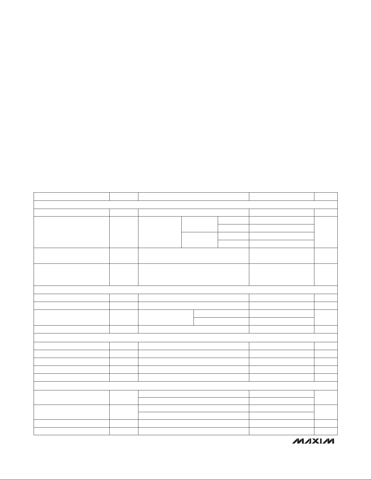
Typical Application Circuit
+
Denotes a lead(Pb)-free/RoHS-compliant package.
For pricing, delivery, and ordering information, please contact Maxim Direct at 1-888-629-4642,
or visit Maxim’s website at www.maxim-ic.com.
MAX3140
SPI/
MICRO-
WIRE
CS
SCLK
UART
DIN
µP
DOUT
IRQ
CONTROL
LOGIC
RS-485
RS-422
R
t
R
t
H/F SRL
TXP
RXP
HALF/FULL-DUPLEX
RS-485/RS-422
MAX3140
SPI/MICROWIRE-Compatible UART with Integrated
True Fail-Safe RS-485/RS-422 Transceivers
2 _______________________________________________________________________________________
ABSOLUTE MAXIMUM RATINGS
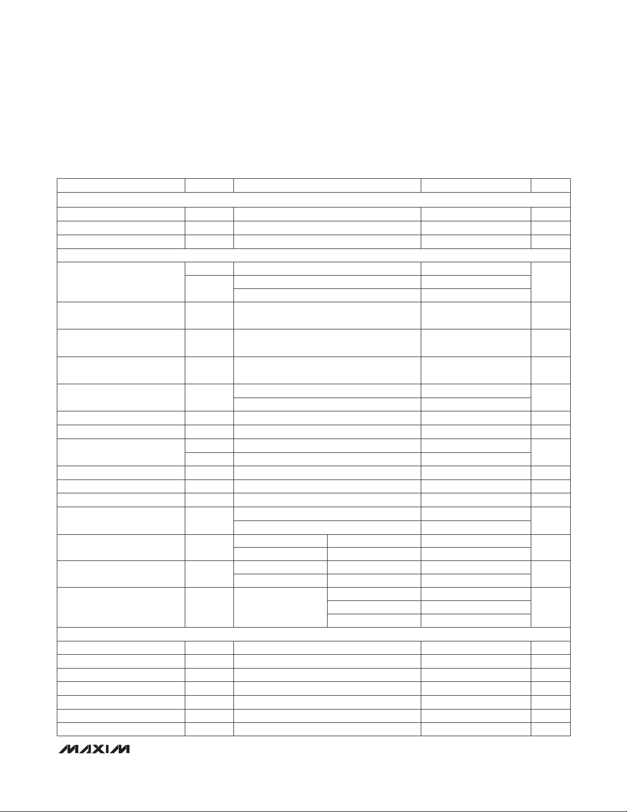
ELECTRICAL CHARACTERISTICS
(VCC= +5V ±5%, DE = VCC, RE = GND, SHDN = VCC, f
XTL
= 1.8432MHz, TA= T
MIN
to T
MAX
, unless otherwise noted. Typical values
are measured with V
CC
= +5V, UART configured for 9600 baud, TA= +25°C.) (Note 1)
Stresses beyond those listed under “Absolute Maximum Ratings” may cause permanent damage to the device. These are stress ratings only, and functional
operation of the device at these or any other conditions beyond those indicated in the operational sections of the specifications is not implied. Exposure to
absolute maximum rating conditions for extended periods may affect device reliability.
VCCto GND ..........................................................................+6V
Input Voltage to GND (CS, SHDN, X1, CTS, RX, DIN, SCLK,
RE, DE, H/F, SRL, TXP, RXP, Dl) .............-0.3V to (V
CC
+ 0.3V)
Output Voltage to GND
DOUT, RTS, TX, X2, RO...........................-0.3V to (V
CC
+ 0.3V)
IRQ ........................................................................-0.3V to +6V
Driver Output Voltage (Y, Z) ...............................................±13V
Receiver Input Voltage, Half Duplex (Y, Z)......................... ±13V
Receiver Input Voltage, Full Duplex (A, B) .........................±25V
TX, RTS Output Current ...................................................100mA
X2, DOUT, IRQ Short-Circuit Duration
(to V
CC
or GND) ......................................................Continuous
Continuous Power Dissipation (T
A
= +70°C)
28-pin QSOP (derate 10.8mW/°C above +70°C)..........860mW
Operating Temperature Ranges
MAX3140CEI .......................................................0°C to +70°C
MAX3140EEI ....................................................-40°C to +85°C
Storage Temperature Range .............................-65°C to +150°C
Lead Temperature (soldering, 10sec) .............................+300°C
Soldering Temperature (reflow) .......................................+260°C
I
SOURCE
= 5mA; DOUT, RTS
SHDN = GND or SHDNi bit = 1;
DE = GND; RE = V
CC
SHDN = GND or SHDNi bit = 1
CONDITIONS
VCC- 0.5
pF5C
IN2
Input Capacitance
µA±1I
LKG1
Input Leakage Current
mV250V
HYST2
Input Hysteresis
V0.3V
CC
V
IL2
Input Low Voltage
V0.7V
CC
V
IH2
Input High Voltage
pF5C
IN1
Input Capacitance
25
V0.2V
CC
V
IL1
Input Low Voltage
V0.7V
CC
V
IH1
Input High Voltage
0.64 1.6
0.7 1.9
µA20
I
CC
SHDN
(FULL)
Supply Current with Both
RS-485 Transceiver and UART
Shut Down
0.74 2
mA
0.69 1.8
I
CC
Supply Current
mA0.47 1
I
CC
SHDN
UART
Supply Current with Only UART
Shut Down
UNITSMIN TYP MAXSYMBOLPARAMETER
I
SINK
= 4mA; DOUT, RTS
I
SOURCE
= 10mA; TX only
0.4
V
VCC- 0.5
V
OH1
Output High Voltage
V4.75 5.25V
CC
Supply Voltage
VX1= 0 or V
CC
µA
2
I
IN1
Input Current
SHDNi bit = 0
SHDNi bit = 1
I
SINK
= 25mA; TX only
V
0.9
V
OL1
Output Low Voltage
CS = VCC; D
OUT
only
µA
5
I
LKG2
Output Leakage ±1
C
OUT1
Output Capacitance pF
SHDN = VCC;
SHDNi bit = 0,
no load
DE = V
CC
DE = GND
DE = V
CC
DE = GND
SRL = V
CC
SRL = GND
or open
UART OUTPUTS (DOUT, TX, RTS)
UART LOGIC INPUTS (DIN, SCLK, CS, SHDN, CTS, RX)
UART OSCILLATOR INPUT (X1)
POWER SUPPLY
MAX3140
SPI/MICROWIRE-Compatible UART with Integrated
True Fail-Safe RS-485/RS-422 Transceivers
_______________________________________________________________________________________ 3
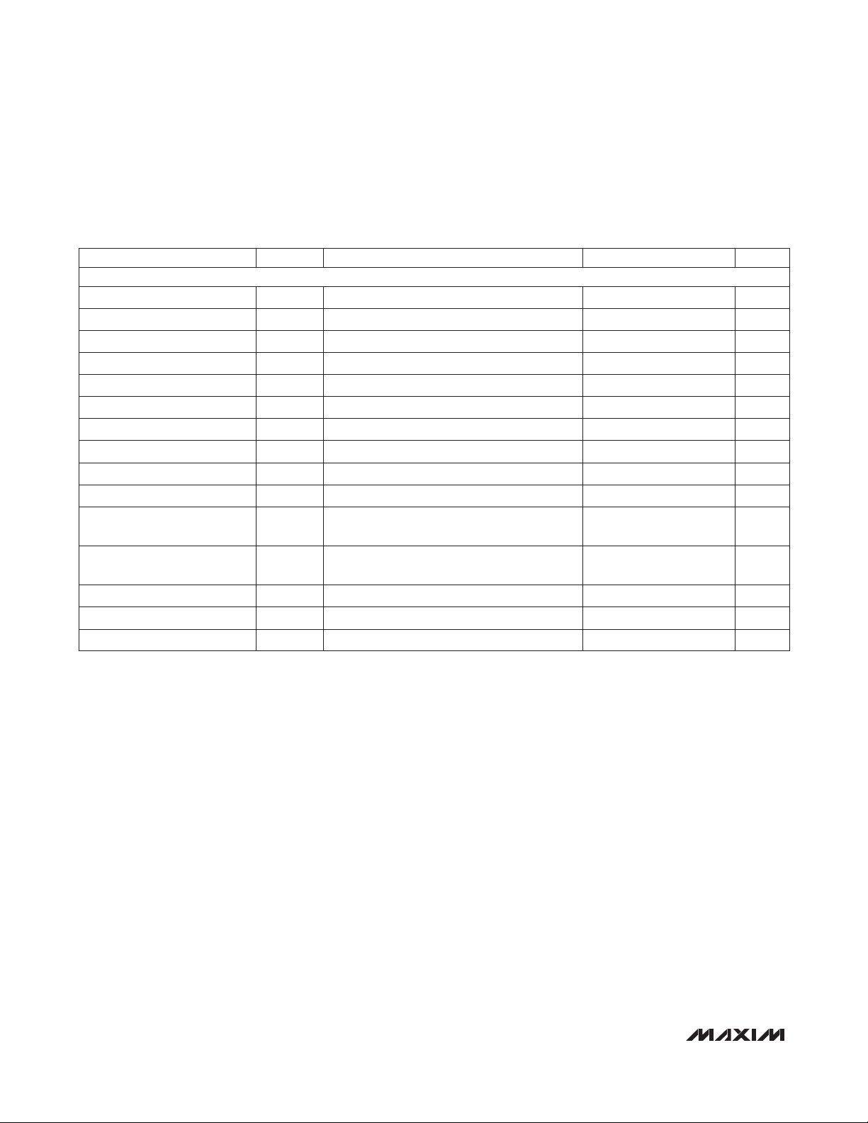
ELECTRICAL CHARACTERISTICS (continued)
(VCC= +5V ±5%, DE = VCC, RE = GND, SHDN = VCC, f
XTL
= 1.8432MHz, TA= T
MIN
to T
MAX
, unless otherwise noted. Typical values
are measured with V
CC
= +5V, UART configured for 9600 baud, TA= +25°C.) (Note 1)
R = 50Ω or R = 27Ω, Figure 1
R = 50Ω or R = 27Ω, Figure 1 (Note 2)
R = 27Ω (RS-422), Figure 1
R = 50Ω (RS-422), Figure 1
No load, Figure 1
V
IRQ
= V
CC
I
SINK
= 4mA
R = 50Ω or R = 27Ω, Figure 1 (Note 2)
CONDITIONS
V3V
OC
Common-Mode Output
Voltage
V0.2ΔV
OD
Change in Magnitude of
Differential Output Voltage
V
1.5
V
OD2
Differential Output Voltage
2.0
5V
OD1
pF5C
OUT2
Output Capacitance
µA±1I
LKG3
Output Leakage
V0.4V
OL2
Output Low Voltage
V0.2ΔV
OC
Change In Magnitude of
Common-Mode Voltage
UNITSMIN TYP MAXSYMBOLPARAMETER
(Note 3)
H/F, TXP, RXP, internal pull-down
DE, DI, RE
SRL = VCCor unconnected
DE, Dl, RE, H/F, TXP, RXP
DE, Dl, RE
SRL = GND (Note 3)
SRL = V
CC
V
0.4 · V
CC
0.6 · V
CC
V
IM2
SRL Input Middle Voltage
VVCC- 0.8V
IH2
SRL Input High Voltage
µA
10 40I
IN2
Input Current
±2I
IN1
mV100V
HYS
DI Input Hysteresis
V0.8V
IL1
Input Low Voltage
2.0
µA
-75
I
IN3
SRL Input Current
75
V0.8V
IL2
SRL Input Low Voltage
(Note 4)
DE = GND
VCC= GND or 5.25V
DE = GND
250
-250
µA
125
I
O
Full-Duplex Output Leakage
(Y and Z)
µA
-75
I
IN4
125
Full-Duplex Input Current
(A and B)
mA
±25
I
OSD
Short-Circuit Output Current
-7V ≤ VCM≤ +12V mV-200 -125 -50V
TH
mV25ΔV
TH
Input Hysteresis
Differential Threshold Voltage
I
SINK
= 4mA, VID= -200mV
I
SOURCE
= 4mA, VID= -50mV
0.4V ≤ VO≤ 2.4V
V0.4V
OL
VVCC- 1.5V
OH
µA±1I
OZR
Output High Voltage
Three-State Output Current
Output Low Voltage
-7V ≤ VCM≤ 12V
0 ≤ VRO≤ V
CC
kΩ96R
IN
mA±7 ±95I
OSR
Output Short-Circuit Current
Input Resistance
VIN= 12V
VIN= -7V
VCC= GND or 5.25V
VIN= 12V
VIN= -7V -100
-7V ≤ V
OUT
≤ V
CC
0 ≤ V
OUT
≤ 12V
0 ≤ V
OUT
≤ V
CC
H/F, TXP, RXP
V
2.4
V
IH1
Input High Voltage
UART IRQ OUTPUT (Open Drain)
RS-485 DRIVER
RS-485 RECEIVER
MAX3140
SPI/MICROWIRE-Compatible UART with Integrated
True Fail-Safe RS-485/RS-422 Transceivers
4 _______________________________________________________________________________________
UART SWITCHING CHARACTERISTICS
(VCC= +5V ±5%, f
XTL
= 1.8432MHz, TA= T
MIN
to T
MAX
, unless otherwise noted. Typical values are measured with VCC= +5V,
UART configured for 9600 baud, T
A
= +25°C.) (Note 1)
CONDITIONS UNITSMIN TYP MAXSYMBOLPARAMETER
C
LOAD
= 100pF ns100t
DV
CS Low to DOUT Valid
C
LOAD
= 100pF, RCS= 10kΩ ns100t
TR
CS High to DOUT Tri-State
ns0t
CSH
CS to SCLK Hold Time
ns100t
CSS
CS to SCLK Setup Time
ns100t
DS
DIN to SCLK Setup Time
ns238t
CP
SCLK Period
ns0t
DH
DIN to SCLK Hold Time
C
LOAD
= 100pF ns100t
DO
SCLK Fall to DOUT Valid
ns100t
CL
SCLK Low Time
ns200t
CS1
CS Rising Edge to SCLK
Rising
ns100t
CS0
SCLK Rising Edge to CS
FaIling
TX, RTS, DOUT; C
LOAD
= 100pF
ns10t
r
Output Rise Time
TX, RTS, DOUT, IRQ; C
LOAD
= 100pF
ns10t
f
Output Fall Time
ns200t
CSW
CS High Pulse Width
ns100t
CH
SCLK High Time
UART AC TIMING (Figure 1)

MAX3140
SPI/MICROWIRE-Compatible UART with Integrated
True Fail-Safe RS-485/RS-422 Transceivers
_______________________________________________________________________________________ 5
SWITCHING CHARACTERISTICS—SRL = Unconnected
(VCC= +5V ±5%, TA= T
MIN
to T
MAX
, unless otherwise noted. Typical values are at VCC= +5V and TA= +25°C.)
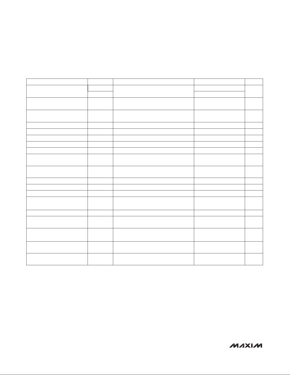
500 2030 2600
t
DPHL
PARAMETER SYMBOL MIN TYP MAX UNITS
Driver Disable Time from Low t
DLZ
100 ns
Driver Enable to Output Low t
DZL
3500 ns
Driver Enable to Output High t
DZH
3500 ns
Maximum Data Rate f
MAX
115 kbps
Driver Disable Time from High t
DHZ
100 ns
Receiver Input to Output
t
RPLH
,
t
RPHL
127 200 ns
|
t
RPLH
- t
RPHL
|
Differential
Receiver Skew
t
RSKD
3±30ns
Receiver Enable to Output Low t
RZL
20 50 ns
Driver Output Skew
|
t
DPLH
- t
DPHL
|
Driver Input to Output
t
DPLH
500 2030 2600
ns
t
DSKEW
-3 ±200 ns
Driver Rise or Fall Time tDR, t
DF
667 1320 2500 ns
Receiver Enable to Output High t
RZH
20 50 ns
Receiver Disable Time from Low t
RLZ
20 50 ns
Receiver Disable Time from
High
t
RHZ
20 50 ns
Time to Shutdown t
SHDN
50 200 600 ns
Driver Enable from Shutdown to
Output High
t
DZH(SHDN)
6000 ns
Driver Enable from Shutdown to
Output Low
t
DZL(SHDN)
6000 ns
Receiver Enable from Shutdown
to Output High
t
RZH(SHDN)
3500 ns
Receiver Enable from Shutdown
to Output Low
t
RZL(SHDN)
3500 ns
CONDITIONS
Figures 2 and 8, CL= 100pF, S2 closed
Figures 4 and 6, CL= 15pF, S1 closed
Figures 2 and 8, CL= 100pF, S1 closed
Figures 4 and 6, CL= 100pF, S1 closed
Figures 4 and 6, CL= 100pF, S2 closed
Figures 4 and 6, CL= 15pF, S2 closed
Figures 7 and 9, |V
ID
|
≥ 2.0V,
rise and fall time of V
ID
≤ 15ns
Figures 2 and 8, CL= 100pF, S2 closed
(Note 5)
Figures 7 and 9, |V
ID
|
≥ 2.0V,
rise and fall time of V
ID
≤ 15ns
Figures 2 and 8, CL= 100pF, S1 closed
Figures 4 and 6, CL= 15pF, S2 closed
Figures 4 and 6, CL= 15pF, S1 closed
Figures 2 and 8, CL= 100pF, S2 closed
Figures 3 and 5, R
DIFF
= 54Ω,
CL1= CL2= 100pF
Figures 2 and 8, CL= 100pF, S1 closed
Figures 3 and 5, R
DIFF
= 54Ω,
C
L1
= CL2= 100pF
Figures 3 and 5, R
DIFF
= 54Ω,
CL1= CL2= 100pF
MAX3140
SPI/MICROWIRE-Compatible UART with Integrated
True Fail-Safe RS-485/RS-422 Transceivers
6 _______________________________________________________________________________________
SWITCHING CHARACTERISTICS—SRL = V
CC
(VCC= +5V ±5%, TA= T
MIN
to T
MAX
, unless otherwise noted. Typical values are at VCC= +5V and TA= +25°C.)
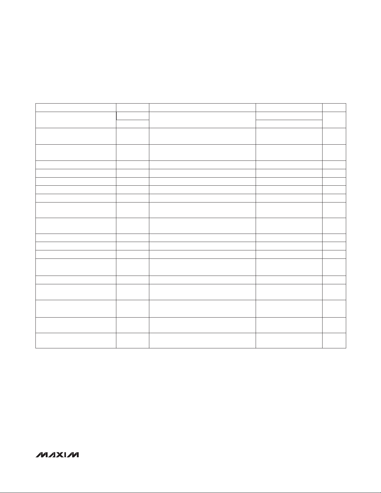
250 720 1000
Receiver Enable from Shutdown
to Output Low
t
RZL(SHDN)
3500 nsFigures 2 and 8, CL= 100pF, S1 closed
t
DPHL
PARAMETER SYMBOL MIN TYP MAX UNITS
Driver Disable Time from Low t
DLZ
100 ns
Driver Enable to Output Low t
DZL
2500 ns
Driver Enable to Output High t
DZH
2500 ns
Maximum Data Rate f
MAX
500 kbps
Driver Disable Time from High t
DHZ
100 ns
Receiver Input to Output
t
RPLH
,
t
RPHL
127 200 ns
|
t
RPLH
- t
RPHL
|
Differential
Receiver Skew
t
RSKD
3±30ns
Receiver Enable to Output Low t
RZL
20 50 ns
Driver Output Skew
|
t
DPLH
- t
DPHL
|
Driver Input to Output
t
DPLH
250 720 1000
ns
t
DSKEW
-3 ±100 ns
Driver Rise or Fall Time t
DR, tDF
200 530 950 ns
Receiver Enable to Output High t
RZH
20 50 ns
Receiver Disable Time from Low t
RLZ
20 50 ns
Receiver Disable Time from
High
t
RHZ
20 50 ns
Time to Shutdown t
SHDN
50 200 600 ns
Driver Enable from Shutdown to
Output High
t
DZH(SHDN)
4500 ns
Driver Enable from Shutdown to
Output Low
t
DZL(SHDN)
4500 ns
Receiver Enable from Shutdown
to Output High
t
RZH(SHDN)
3500 ns
CONDITIONS
Figures 2 and 8, CL= 100pF, S2 closed
Figures 4 and 6, CL= 15pF, S1 closed
Figures 2 and 8, CL= 100pF, S1 closed
Figures 4 and 6, CL= 100pF, S1 closed
Figures 4 and 6, CL= 100pF, S2 closed
Figures 4 and 6, CL= 15pF, S2 closed
Figures 7 and 9, |V
ID
|
≥ 2.0V,
rise and fall time of V
ID
≤ 15ns
Figures 2 and 8, CL= 100pF, S2 closed
(Note 5)
Figures 7 and 9, |V
ID
|
≥ 2.0V,
rise and fall time of V
ID
≤ 15ns
Figures 2 and 8, CL= 100pF, S1 closed
Figures 4 and 6, CL= 15pF, S2 closed
Figures 4 and 6, CL= 15pF, S1 closed
Figures 2 and 8, CL= 100pF, S2 closed
Figures 3 and 5, R
DIFF
= 54Ω,
C
L1
= CL2= 100pF
Figures 3 and 5, R
DIFF
= 54Ω,
C
L1
= CL2= 100pF
Figures 3 and 5, R
DIFF
= 54Ω,
CL1= CL2= 100pF
MAX3140
SPI/MICROWIRE-Compatible UART with Integrated
True Fail-Safe RS-485/RS-422 Transceivers
_______________________________________________________________________________________ 7
SWITCHING CHARACTERISTICS—SRL = GND
(VCC= +5V ±5%, TA= T
MIN
to T
MAX
, unless otherwise noted. Typical values are at VCC= +5V and TA= +25°C.)
PARAMETER SYMBOL MIN TYP MAX UNITS
Driver Disable Time from Low t
DLZ
100 ns
Driver Enable to Output Low t
DZL
150 ns
Driver Enable to Output High t
DZH
150 ns
Maximum Data Rate f
MAX
10 Mbps
Driver Disable Time from High t
DHZ
100 ns
Receiver Input to Output
t
RPLH
,
t
RPHL
106 150 ns
|
t
RPLH
- t
RPHL
|
Differential
Receiver Skew
t
RSKD
0±10ns
Receiver Enable to Output Low t
RZL
20 50 ns
Driver Output Skew
|
t
DPLH
- t
DPHL
|
Driver Input to Output
t
DPLH
34 60
ns
t
DSKEW
-2.5 ±10 ns
Driver Rise or Fall Time t
DR, tDF
14 25 ns
Receiver Enable to Output High t
RZH
20 50 ns
Receiver Disable Time from Low t
RLZ
20 50 ns
Receiver Disable Time from
High
t
RHZ
20 50 ns
Time to Shutdown t
SHDN
50 200 600 ns
Driver Enable from Shutdown to
Output High
t
DZH(SHDN)
250 ns
Driver Enable from Shutdown to
Output Low
t
DZL(SHDN)
250 ns
Receiver Enable from Shutdown
to Output High
t
RZH(SHDN)
3500 ns
34 60
CONDITIONS
Figures 2 and 8, CL= 100pF, S2 closed
Figures 4 and 6, CL= 15pF, S1 closed
Figures 2 and 8, CL= 100pF, S1 closed
Figures 4 and 6, CL= 100pF, S1 closed
Figures 4 and 6, CL= 100pF, S2 closed
Figures 4 and 6, CL= 15pF, S2 closed
Figures 7 and 9, |V
ID
|
≥ 2.0V,
rise and fall time of V
ID
≤ 15ns
Figures 2 and 8, CL= 100pF, S2 closed
(Note 5)
Figures 7 and 9, |V
ID
|
≥ 2.0V,
rise and fall time of V
ID
≤ 15ns
Figures 2 and 8, CL= 100pF, S1 closed
Figures 4 and 6, CL= 15pF, S2 closed
Figures 4 and 6, CL= 15pF, S1 closed
Figures 2 and 8, CL= 100pF, S2 closed
Figures 3 and 5, R
DIFF
= 54Ω,
C
L1
= CL2= 100pF
Receiver Enable from Shutdown
to Output Low
Figures 3 and 5, R
DIFF
= 54Ω,
C
L1
= CL2= 100pF
t
RZL(SHDN)
3500
Figures 3 and 5, R
DIFF
= 54Ω,
C
L1
= CL2= 100pF
nsFigures 2 and 8, CL= 100pF, S1 closed
t
DPHL
Note 1: All currents into the device are positive; all currents out of the device are negative. All voltages are referred to device
ground unless otherwise noted.
Note 2: ΔV
OD
and ΔVOCare the changes in VODand VOC, respectively, when the Dl input changes state.
Note 3: The SRL pin is internally biased to V
CC
/2 by a 100kΩ/100kΩ resistor-divider. It is guaranteed to be VCC/2 if left unconnected.
Note 4: Maximum current level applies to peak current just prior to foldback-current limiting; minimum current level applies during
current limiting.
Note 5: The device is put into shutdown by bringing RE high and DE low. If the enable inputs are in this state for less than 50ns, the
device is guaranteed not to enter shutdown. If the enable inputs are in this state for at least 600ns, the device is guaranteed
to have entered shutdown.
MAX3140
SPI/MICROWIRE-Compatible UART with Integrated
True Fail-Safe RS-485/RS-422 Transceivers
8 _______________________________________________________________________________________
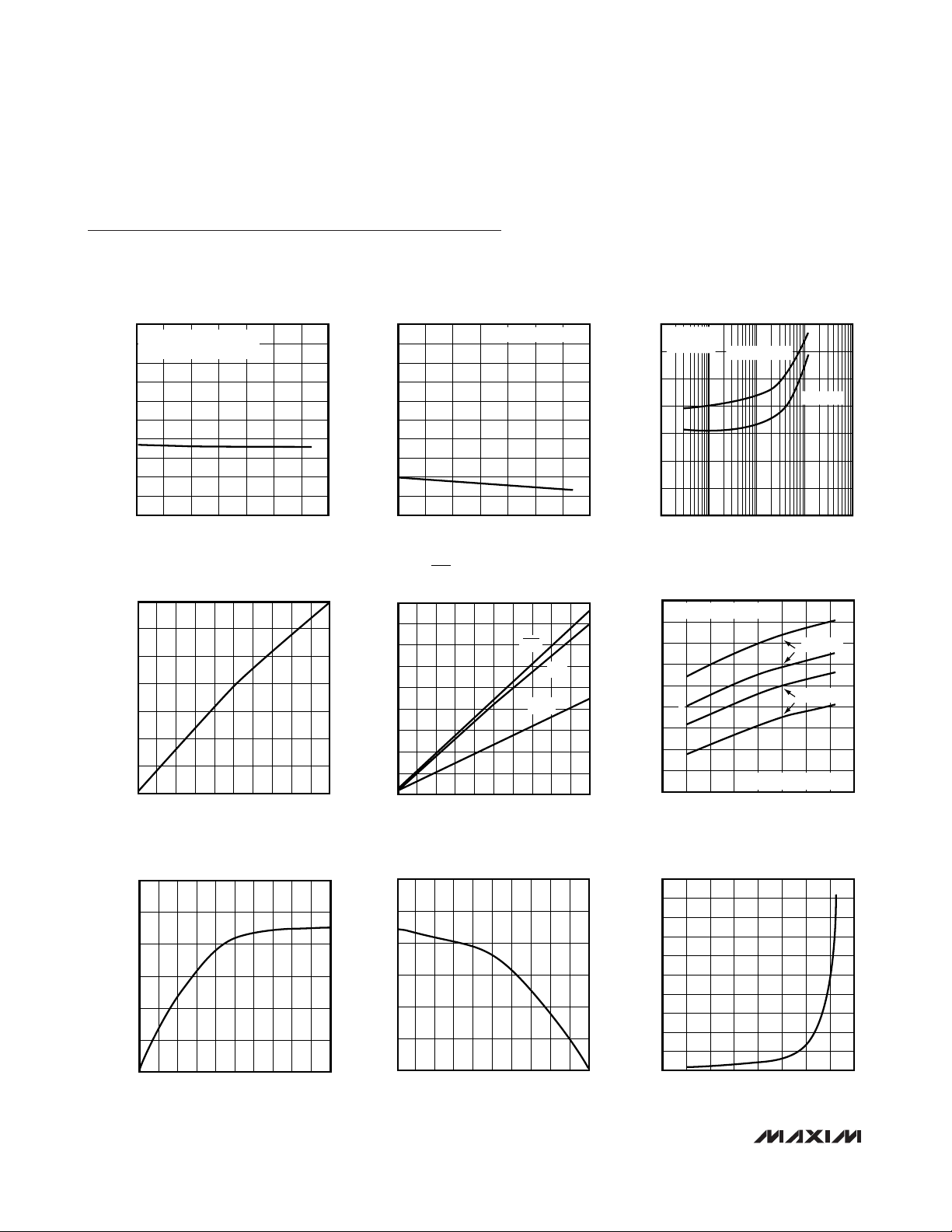
Typical Operating Characteristics
(VCC= +5V, TA = +25°C, unless otherwise noted.)
1000
900
0
-40 -20 40 60 100
UART SUPPLY CURRENT
vs. TEMPERATURE
200
100
800
700
MAX3140-01
TEMPERATURE (°C)
SUPPLY CURRENT (μA)
020 80
600
500
400
300
1.8432MHz CRYSTAL
TRANSMITTING AT 115.2 kbps
10
9
0
-40 -20 40 60 100
UART SHUTDOWN CURRENT
vs. TEMPERATURE
2
1
8
7
MAX3140-02
TEMPERATURE (°C)
SHUTDOWN CURRENT (μA)
020 80
6
5
4
3
1.8432MHz CRYSTAL
400
50
100 10k
1000
100k 1M
UART SUPPLY CURRENT
vs. BAUD RATE
150
100
MAX3140-03
BAUD RATE (bps)
SUPPLY CURRENT (μA)
200
250
350
300
TRANSMITTING
1.8432 MHz
CRYSTAL
STANDBY
700
600
0
01 3
4
5
UART SUPPLY CURRENT vs.
EXTERNAL CLOCK FREQUENCY
100
500
MAX3140-04
EXTERNAL CLOCK FREQUENCY (MHz)
SUPPLY CURRENT (μA)
2
400
300
200
0
10
05
RS-485 OUTPUT CURRENT
vs. RECEIVER OUTPUT LOW VOLTAGE
20
60
MAX3140-07
OUTPUT LOW VOLTAGE (V)
OUTPUT CURRENT (mA)
3
40
30
2
50
14
90
80
0
0 0.20.1 0.6 0.7
0.8
1.0
TX, RTS, DOUT OUTPUT CURRENT
vs. OUTPUT LOW VOLTAGE
10
70
MAX3140-05
OUTPUT LOW VOLTAGE (V)
OUTPUT SINK CURRENT (mA)
0.3 0.50.4 0.9
60
50
40
30
20
RTS
TX
DOUT
300
-60 100
RS-485 TRANSCEIVER NO-LOAD
SUPPLY CURRENT vs. TEMPERATURE
350
325
525
MAX3140-06
TEMPERATURE (°C)
NO-LOAD SUPPLY CURRENT (μA)
40
450
425
375
400
060
500
475
-40 -20 20 80
A: SRL = GND
B: SRL = OPEN OR V
CC
A
A
B
DE = V
CC
DE = GND
B
0
5
05
RS-485 OUTPUT CURRENT
vs. RECEIVER OUTPUT HIGH VOLTAGE
10
30
MAX3140-08
OUTPUT HIGH VOLTAGE (V)
OUTPUT CURRENT (mA)
3
20
15
2
25
14
0
2
-60 100
RS-485 TRANSCEIVER SHUTDOWN
CURRENT vs. TEMPERATURE
4
6
20
MAX3140-09
TEMPERATURE (°C)
SHUTDOWN CURRENT (nA)
40
12
14
10
8
060
16
18
-40 -20 20 80
MAX3140
SPI/MICROWIRE-Compatible UART with Integrated
True Fail-Safe RS-485/RS-422 Transceivers
_______________________________________________________________________________________
9
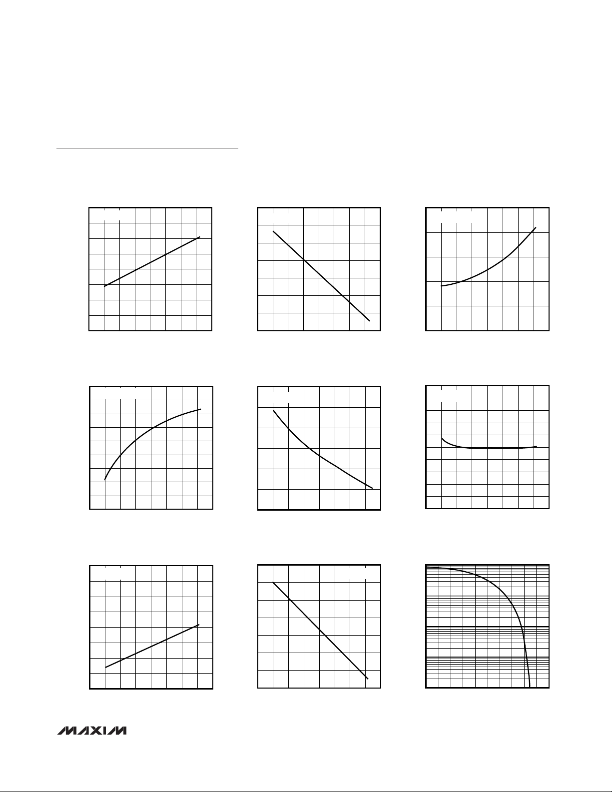
Typical Operating Characteristics (continued)
(VCC= +5V, TA = +25°C, unless otherwise noted.)
0.10
0.15
-60 80 100
RS-485 RECEIVER OUTPUT LOW VOLTAGE
vs. TEMPERATURE
0.20
0.50
MAX3140-10
TEMPERATURE (°C)
OUTPUT LOW VOLTAGE (V)
20
0.40
0.35
0.30
0.25
040
0.45
-40 -20 60
IRO = 8mA
3.8
3.9
-60 80 100
RS-485 RECEIVER OUTPUT HIGH VOLTAGE
vs. TEMPERATURE
4.0
4.5
MAX3140-11
TEMPERATURE (°C)
OUTPUT HIGH VOLTAGE (V)
20
4.3
4.2
4.1
040
4.4
-40 -20 60
IRO = 8mA
115
-60 100
RS-485 RECEIVER PROPAGATION DELAY
(500kbps MODE) vs. TEMPERATURE
120
140
MAX3140-12
TEMPERATURE (°C)
PROPAGATION DELAY (ns)
40
130
125
060
135
-40 -20 20 80
C
LOAD
= 100pF
94
-60 100
RS-485 RECEIVER PROPAGATION DELAY
(10Mbps MODE) vs. TEMPERATURE
98
96
112
MAX3140-13
TEMPERATURE (°C)
PROPAGATION DELAY (ns)
40
106
104
100
102
060
110
108
-40 -20 20 80
C
LOAD
= 100pF
20
25
-60 100
RS-485 DRIVER PROPAGATION DELAY
(10Mbps MODE) vs. TEMPERATURE
30
60
MAX3140-16
TEMPERATURE (°C)
PROPAGATION DELAY (ns)
40
45
50
40
35
060
55
-40 -20 20 80
Rt = 54Ω
1.90
-60 100
RS-485 DRIVER PROPAGATION DELAY
(115kbps MODE) vs. TEMPERATURE
1.95
2.20
MAX3140-14
TEMPERATURE (°C)
PROPAGATION DELAY (μs)
40
2.10
2.00
2.05
060
2.15
-40 -20 20 80
Rt = 54Ω
520
560
-60 100
RS-485 DRIVER PROPAGATION DELAY
(500kbps MODE) vs. TEMPERATURE
600
640
920
MAX3140-15
TEMPERATURE (°C)
PROPAGATION DELAY (ns)
40
760
800
720
680
060
840
880
-40 -20 20 80
Rt = 54Ω
1.83
1.84
-60 100
RS-485 DRIVER DIFFERENTIAL
OUTPUT VOLTAGE vs. TEMPERATURE
1.85
1.90
MAX3140-17
TEMPERATURE (°C)
OUTPUT VOLTAGE (V)
40
1.88
1.87
1.86
060
1.89
-40 -20 20 80
Rt = 54Ω
100
0.01
01
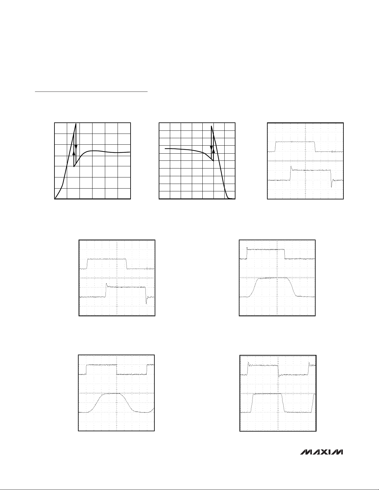
RS-485 DRIVER OUTPUT CURRENT
vs. DIFFERENTIAL OUTPUT VOLTAGE
0.1
10
1
MAX3140-18
DIFFERENTIAL OUTPUT VOLTAGE (V)
OUTPUT CURRENT (mA)
234 5
MAX3140
SPI/MICROWIRE-Compatible UART with Integrated
True Fail-Safe RS-485/RS-422 Transceivers
10 ______________________________________________________________________________________
Typical Operating Characteristics (continued)
(VCC= +5V, TA = +25°C, unless otherwise noted.)
0
20
40
60
80
100
120
140
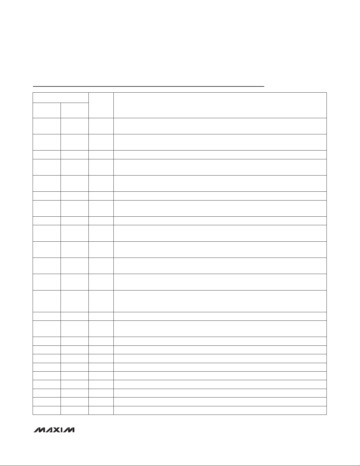
OUTPUT CURRENT vs.
RS-485 DRIVER OUTPUT LOW VOLTAGE
MAX3140-19
OUTPUT LOW VOLTAGE (V)
OUTPUT CURRENT (mA)
024681012
0
-10
-20
-30
-40
-50
-60
-70
-80
-90
-100
-8 -2
OUTPUT CURRENT vs.
RS-485 DRIVER OUTPUT HIGH VOLTAGE
MAX3140-20
OUTPUT HIGH VOLTAGE (V)
OUTPUT CURRENT (mA)
642-6 -4 0
50ns/div
VA - V
B
(2V/div)
RO
(5V/div)
MAX3140-21
RS-485 RECEIVER PROPAGATION DELAY
(SRL = GND)
50ns/div
VA - V
B
(2V/div)
RO
(5V/div)
MAX3140-22
RS-485 RECEIVER PROPAGATION DELAY
(SRL = OPEN OR V
CC
)
2μs/div
RS-485 DRIVER PROPAGATION DELAY
(SRL = OPEN)
DI
(5V/div)
V
Y
- V
Z
(2.5V/div)
MAX3140-23
500ns/div
RS-485 DRIVER PROPAGATION DELAY
(SRL = V
CC
)
DI
(5V/div)
V
Y
- V
Z
(2.5V/div)
MAX3140-24
50ns/div
RS-485 DRIVER PROPAGATION DELAY
(SRL = GND)
DI
(5V/div)
V
Y
- V
Z
(2.5V/div)
MAX3140-25
MAX3140
SPI/MICROWIRE-Compatible UART with Integrated
True Fail-Safe RS-485/RS-422 Transceivers
______________________________________________________________________________________ 11
Pin Description
UART Crystal Connection. Leave X2 unconnected for external clock. See the
Crystals,
Oscillators, and Ceramic Resonators
section.
X21 1
2
UART Crystal Connection. X1 also serves as an external clock input. See the
Crystals,
Oscillators, and Ceramic Resonators
section.
X12
3
4
UART Request-to-Send Active-Low Output. Controlled by the RTS bit. Use to control the driver enable in RS-485 networks.
RTS
4
UART Clear-to-Send Active-Low Input. Read via the CTS bit.
CTS
3
5
6 UART Asynchronous Serial-Data (transmitter) OutputTX6
7
8 GroundGND8
RS-485 Half/Full-Duplex Selector Pin. Connect H/F to VCCfor half-duplex mode; connect H/F
to GND or leave it unconnected for full-duplex mode.
H/F
7
UART Asynchronous Serial-Data (receiver) Input. The serial information received from the modem
or RS-232/RS-485 receiver. A transition on RX while in shutdown generates an interrupt (Table 1).
RX5
9
10
RS-485 Receiver Output Enable. Drive RE low to enable RO; RO is high impedance when RE
is high. Drive RE high and DE low to enter low-power shutdown mode.
RE
10
11
12
RS-485 Driver Input. With DE high, a low on DI forces noninverting output low and inverting
output high. Similarly, a high on DI forces noninverting output high and inverting output low.
DI12
RS-485 Driver Output Enable. Drive DE high to enable driver outputs. These outputs are high
impedance when DE is low. Drive RE high and DE low to enter low-power shutdown mode.
DE11
13
14 No Connection. Not internally connected.N.C.14
15
— RS-485 Noninverting Driver OutputY16
RS-485 Transmitter Phase. Connect TXP to GND or leave it unconnected for normal transmitter phase/polarity. Connect TXP to VCCto invert the transmitter phase/polarity.
TXP15
RS-485 Transceiver Slew-Rate-Limit Selector Pin. Connect SRL to GND for a 10Mbps communication rate, connect SRL to V
CC
for a 500kbps rate, or leave SRL unconnected for a
115kbps rate.
SRL13
RS-485 Receiver Output. When RE is low and if A - B ≥ -50mV, RO will be high; if A - B ≤
-200mV, RO will be low.
RO9
16
17 No Connection. Not internally connected.N.C.17
—
18 RS-485 Inverting Receiver Input and RS-485 Inverting Driver Output*Z—
RS-485 Inverting Driver OutputZ18
—
19 RS-485 Receiver Input Resistors*B—
—
20 RS-485 Receiver Input Resistors*A—
RS-485 Noninverting Receiver InputA20
RS-485 Inverting Receiver InputB19
RS-485 Noninverting Receiver Input and RS-485 Noninverting Driver Output*Y—
FULL
DUPLEX
HALF
DUPLEX
PIN
NAME FUNCTION
 Loading...