Maxim MAX3131EAI, MAX3131CAI, MAX3130EAI, MAX3130CAI Datasheet
For free samples & the latest literature: http://www.maxim-ic.com, or phone 1-800-998-8800.
For small orders, phone 1-800-835-8769.
General Description
The MAX3130/MAX3131 combine an IrDA 1.2 compatible infrared transceiver with an RS-232 interface—all in
a single 3V-powered hybrid microcircuit. The infrared
transceiver supports IrDA data rates of 2.4kbps to
115kbps. The infrared receive channel provides a highgain/low-noise PIN-diode amplifier with 100µA of ambient photodiode current rejection at a +3V supply. A
high-power LED driver capable of sinking 200mA is
included in the infrared transmit path. The on-board
encoder/decoder (ENDEC) compresses/stretches signals to and from the external UART, allowing IrDA communication even with non-IrDA UARTs.
A 2-driver/2-receiver RS-232 transceiver supports data
rates up to 120kbps. A proprietary, high-efficiency, dual
charge-pump power supply and a low-dropout transmitter combine to deliver true RS-232 performance from
a single +3.0V to +5.5V supply. Selectable shutdown
for IR and RS-232 circuitry reduces supply current to
1µA.
The MAX3130 is optimized for applications using a single UART for both infrared and RS-232 communication.
The infrared transmitter input and infrared receiver output are multiplexed with one RS-232 transmitter input
and one RS-232 receiver output, respectively. The
MAX3131’s IrDA transceiver and RS-232 transceivers
are separate and have their own data inputs and outputs.
Both these devices require a minimum of external components: four small 0.1µF capacitors, a photodiode, an
infrared LED, and a current-setting resistor.
Applications
Personal Digital Assistants (PDAs)
Palmtop Computers
Battery-Powered Systems
Hand-Held Equipment
Peripherals
IrDA Applications
Cellular Phones
Features
♦ Integrated RS-232 and IrDA in Single 28-Pin SSOP
Package
♦ 370µA Supply Current
♦ IrDA 1.2 Compatible: 2.4kbps to 115kbps
Data Rate
♦ On-Board IR Encoder/Decoder Allows Use of
Non-IrDA UARTs
♦ +3.0V to +5.5V Single-Supply Operation
♦ Meet EIA/TIA-232 Specifications Down to +3V
♦ 200mA, High-Current Infrared LED Drive
♦ 1µA Low-Power Shutdown with RS-232
Receivers Active
MAX3130/MAX3131
3V to 5.5V, IrDA Infrared Transceiver with
Integrated RS-232 Interface
________________________________________________________________
Maxim Integrated Products
1
28
27
26
25
24
23
22
21
20
19
18
17
16
15
1
2
3
4
5
6
7
8
9
10
11
12
13
14
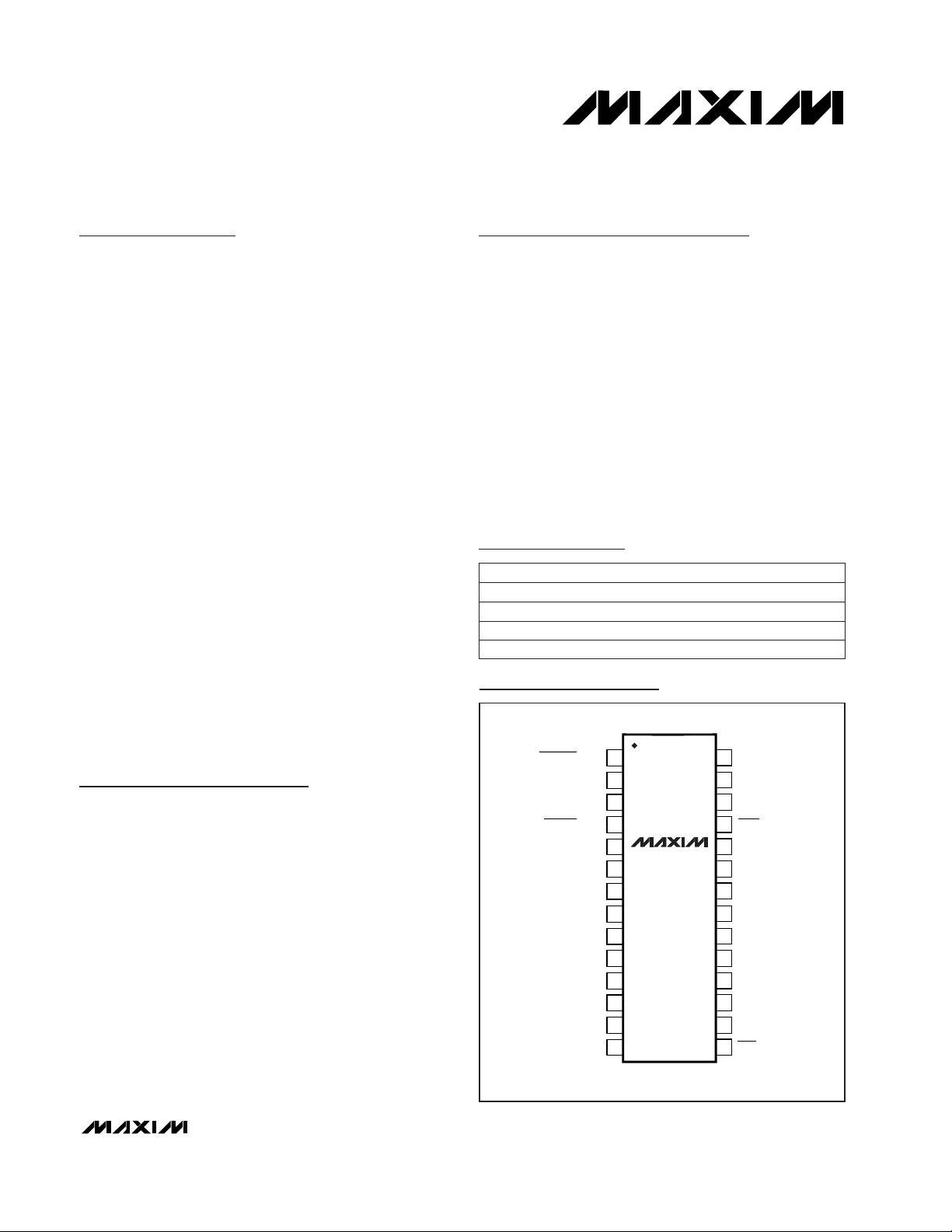
R2OUT
R2IN
T2OUT
RSSD
VC2-
IRSD
C2+
C1C1+
V+
N.C.
LEDC
PGND
PINC
AGND
AV
CC
N.C.
V
CC
GND
BAUD16
T1OUT
R1IN
R1OUT
IRMODE (TXD)
T2IN
T1IN
EDGEDET (RXD)
SSOP
TOP VIEW
MAX3130
MAX3131
( ) ARE FOR MAX3131
19-1402; Rev 0; 11/98
PART
MAX3130CAI
MAX3130EAI
MAX3131CAI
0°C to +70°C
-40°C to +85°C
0°C to +70°C
TEMP. RANGE PIN-PACKAGE
28 SSOP
28 SSOP
28 SSOP
Pin Configuration
Ordering Information
MAX3131EAI -40°C to +85°C 28 SSOP
µA
MAX3130/MAX3131
3V to 5.5V, IrDA Infrared Transceiver with
Integrated RS-232 Interface
2 _______________________________________________________________________________________
ABSOLUTE MAXIMUM RATINGS
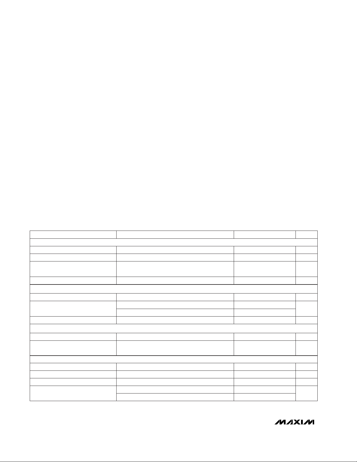
ELECTRICAL CHARACTERISTICS
(VCC= AVCC= 3.0V to 5.5V, GND = AGND = PGND, C1–C4 = 0.1µF (Note 1), TA= T
MIN
to T
MAX
, unless otherwise noted. Typical
values are at T
A
= +25°C and VCC= AVCC= 3.3V.)
Stresses beyond those listed under “Absolute Maximum Ratings” may cause permanent damage to the device. These are stress ratings only, and functional
operation of the device at these or any other conditions beyond those indicated in the operational sections of the specifications is not implied. Exposure to
absolute maximum rating conditions for extended periods may affect device reliability.
VCCto GND..............................................................-0.3V to +6V
AV
CC
to AGND.........................................................-0.3V to +6V
V
CC
to AVCC.......................................................................±0.3V
AGND, PGND to GND ........................................................±0.1V
V+ to GND................................................................-0.3V to +7V
V- to GND.................................................................+0.3V to -7V
V+ to V-................................................................................+13V
Inputs (referenced to GND)
T1IN, T2IN, TXD,
RSSD, IRMODE, BAUD16,
IRSD....................................................................-0.3V to +6V
R1IN, R2IN .....................................................................±25V
Outputs (referenced to GND)
T1OUT, T2OUT............................................................±13.2V
R1OUT, R2OUT, EDGEDET, RXD.........-0.3V to (V
CC
+ 0.3V)
LEDC...................................................................-0.3V to +6V
Output Short-Circuit Duration (to V
CC
or GND)
T1OUT, T2OUT.....................................................Continuous
Output Currents
LEDC Continuous........................................................200mA
LEDC 20% Duty Cycle t
ON
< 90µs..............................500mA
Input Current
PINC..............................................................................10mA
Continuous Power Dissipation (T
A
= +70°C)
SSOP (derate 9.52mW/°C above +70°C)...................762mW
Operating Temperature Ranges
MAX3130/MAX3131CAI ....................................0°C to +70°C
MAX3130/MAX3131EAI..................................-40°C to +85°C
Storage Temperature Range.............................-65°C to +160°C
Lead Temperature (soldering, 10sec).............................+300°C
±0.01 ±1.0
2.4
120 200
Output Voltage Low I
SINK
= 1.6mA
0.25 1.0
0.1 0.4 V
Output Voltage High I
SOURCE
= 1.0mA
VCC-VCC-
0.6 0.05
V
2.0
0.8
1.0 10
0.01 1.0
MIN TYP MAX
Data Rate (Note 3)
µAVIN= 0 to V
CC
Input Leakage Current
2.4 115.2
VCC= AVCC= 5V
kbps
Equivalent Input Noise Current 10 nA
RMS
Input Current Sensitivity (Note 3) 0.0002 6 mA
Ambient Photodiode Current
Rejection
AVCC= 3.3V 100
AVCC= 5V 375
µA
V
VCC= AVCC= 3.3V
Input Logic Threshold High
VInput Logic Threshold Low
µATA= +25°C (Note 2)Analog Power-Supply Current
mAVCC= 3.3V or 5V, TA= +25°C (Note 2)Power-Supply Current
RSSD = low or IRMODE = low,
T
A
= +25°C (Note 2)
Shutdown Supply Current µA
µA
IRSD = low, TA= +25°C (Note 2)
Shutdown Analog Supply Current
UNITSCONDITIONSPARAMETER
LOGIC INPUTS (T1IN, T2IN, TXD, IRMODE, BAUD16, IRSD, RSSD)
DC CHARACTERISTICS
LOGIC OUTPUTS (R1OUT, R2OUT, RXD, EDGEDET)
IR RECEIVER
MAX3130/MAX3131
3V to 5.5V, IrDA Infrared Transceiver with
Integrated RS-232 Interface
_______________________________________________________________________________________ 3
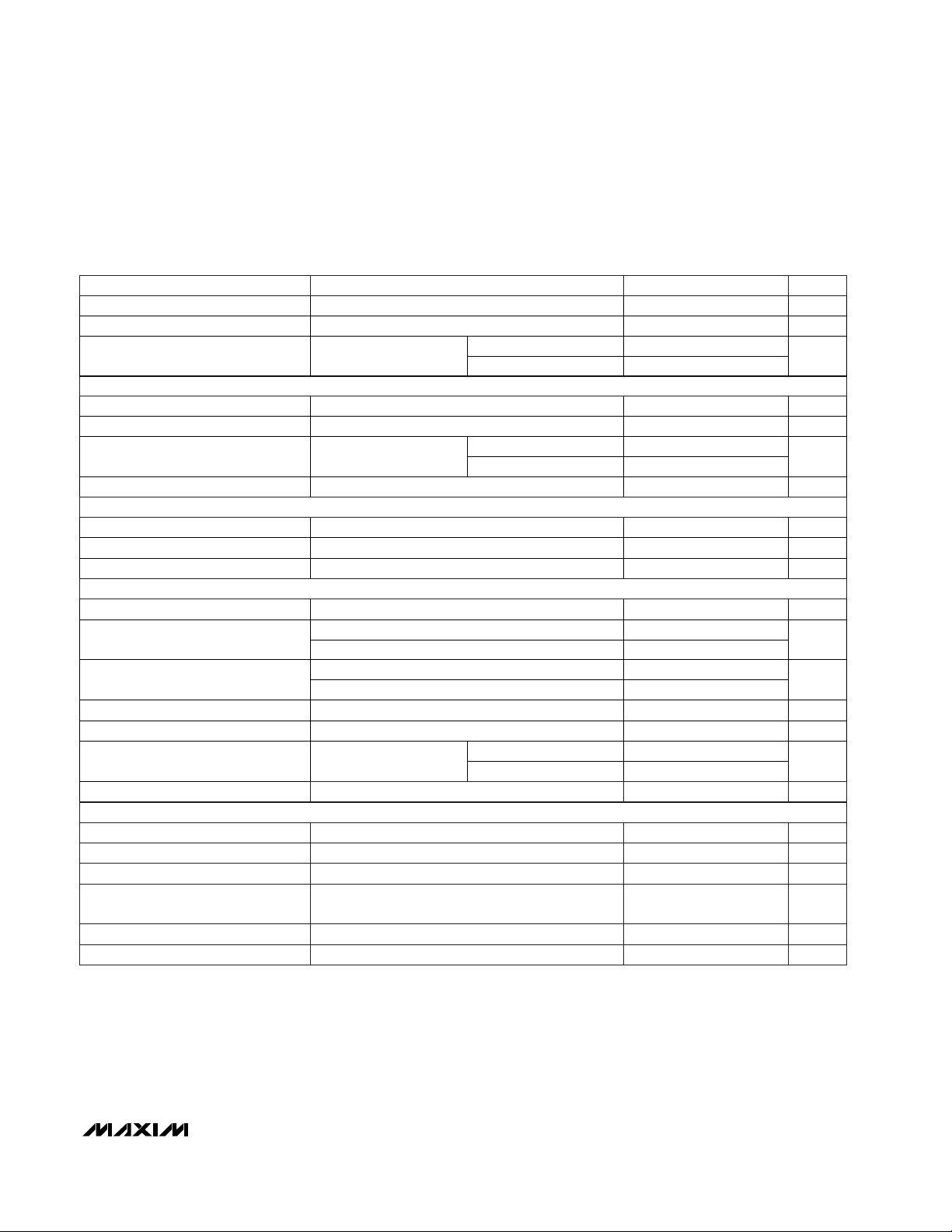
ELECTRICAL CHARACTERISTICS (continued)
(VCC= AVCC= 3.0V to 5.5V, GND = AGND = PGND, C1–C4 = 0.1µF (Note 1), TA= T
MIN
to T
MAX
, unless otherwise noted. Typical
values are at T
A
= +25°C and VCC= AVCC= 3.3V.)
Data rate = 2.4kbps
Data rate = 115kbps
AVCC= 3.3V
IR Receiver Disable Time Delay until I
AVCC
< 1µA 10 µs
IR Receiver Enable Time Delay until maximum IR receive data rate is valid 300 µs
IR Receiver Output Pulse Width
BAUD16 = static
(Note 3)
190
µs
AVCC= 5V
1 1.6 8
IR TRANSMITTER
Transmitter Rise Time 10% to 90% of 200mA drive current 20 600 ns
Transmitter Fall Time 90% to 10% of 200mA drive current 20 600 ns
Transmitter Output Resistance I
OUT
= 200mA
1.15 2
Ω
0.9 1.6
µs
Off-Leakage Current
1.43 2.23
V
LEDC
= 5.5V
t
PHL
t
PLH
0.01 10.0 µA
IrDA ENCODER/DECODER (ENDEC)
Maximum Operating Frequency Maximum frequency at BAUD16 2 MHz
IR Output Pulse Width f
BAUD16
= 1.8432MHz, measured at V
LEDC
BAUD16 Operating Frequency Range f
BAUD16
required to enable ENDEC 34.6 2000 kHz
RS-232 RECEIVER
Input Voltage Range -25 25 V
Input Threshold Low
VCC= 3.3V 0.6 1.2
V
VCC= 5V 0.8 1.5
Input Threshold High
VCC= 3.3V 1.5 2.4
V
VCC= 5V 1.8 2.4
Input Hysteresis 0.3 V
Input Resistance TA= +25°C 357kΩ
Receiver Propagation Delay
R_IN to R_OUT,
CL= 150pF
300
ns
300
Receiver Skew
t
PHL
- t
PLH
, C
L
= 150pF
300 ns
RS-232 TRANSMITTER OUTPUTS
Output Voltage Swing T1OUT, T2OUT, loaded with 3kΩ to GND ±5 ±5.4 V
Output Resistance VCC= V+ = V- = 0, T_OUT = ±2V 300 10M Ω
Output Short-Circuit Current V
T_OUT
= 0 ±35 ±60 mA
Output Leakage Current
V
T_OUT
= ±12V, VCC= 0 to 5.5V,
RS-232 transceiver shutdown
±25 µA
Maximum Data Rate RL= 3kΩ, CL = 1000pF, one transmitter switching 120 235 kbps
Transmitter Skew
t
PHL
- t
PLH
300 ns
PARAMETER CONDITIONS MIN TYP MAX UNITS
IR TRANSMITTER
IrDA ENCODER/DECODER (ENDEC)
RS-232 RECEIVER
RS-232 TRANSMITTER OUTPUTS
MAX3130/MAX3131
3V to 5.5V, IrDA Infrared Transceiver with
Integrated RS-232 Interface
4 _______________________________________________________________________________________
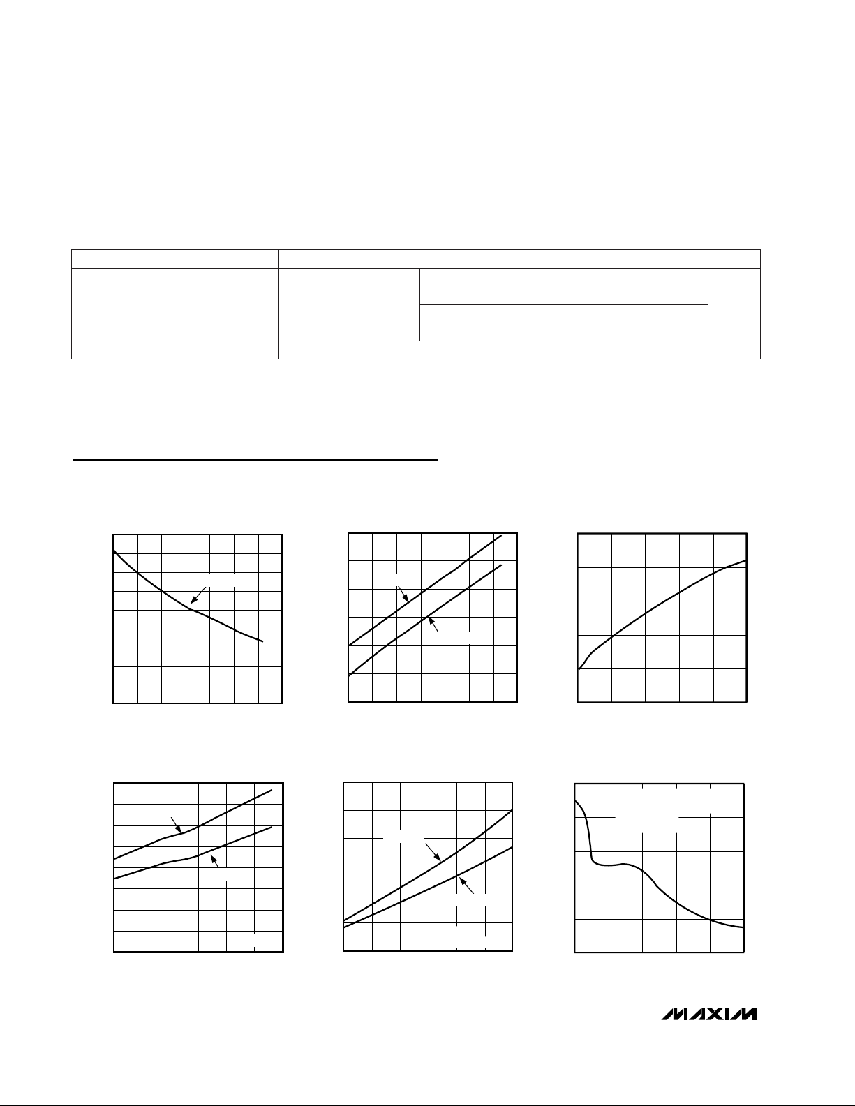
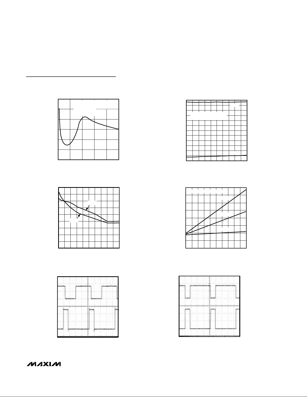
Typical Operating Characteristics
(VCC= AVCC= 3.3V, GND = AGND = PGND, C1–C4 = 0.1µF, RL= 3kΩ, TA = +25°C, unless otherwise noted.)
200
240
220
300
280
260
360
340
320
380
-40 0 20-20 40 60 80 100
SUPPLY CURRENT vs. TEMPERATURE
MAX3130 toc01
TEMPERATURE (°C)
I
CC
(µA)
VCC = 3.3V or 5V
90
110
100
130
120
140
150
-40 20 40-20 0 60 80 100
ANALOG SUPPLY CURRENT
vs. TEMPERATURE
MAX3130 toc02
TEMPERATURE (°C)
I
AVCC
(µA)
AVCC = 5V
AVCC = 3.3V
0
100
300
200
400
500
3.0 4.03.5 4.5 5.0 5.5
AMBIENT PHOTODIODE CURRENT
REJECTION vs. SUPPLY VOLTAGE
MAX3130 toc03
SUPPLY VOLTAGE (V)
CURRENT REJECTION (µA)
0
0.2
0.4
0.6
0.8
1.0
1.2
1.4
1.6
-40 0-20 20 40 80 100
LED DRIVER ON-RESISTANCE
vs. TEMPERATURE
MAX3130 toc04
TEMPERATURE (°C)
R
LED
(Ω)
VCC = 3.3V
VCC = 5V
I
LEDC
= 200mA
0
200
100
400
300
500
600
100 200 250150 300 350 400
LEDC VOLTAGE vs. LEDC CURRENT
MAX3130 toc05
LEDC CURRENT (mA)
LEDC VOLTAGE (mV)
PULSED AT
20% DUTY CYCLE
VCC = 3.3V
VCC = 5V
0
20
60
40
80
100
04020 60 80 100
RXD OUTPUT PULSE WIDTH
vs. DISTANCE (2400bps)
MAX3130 toc06
DISTANCE (cm)
RXD PULSE WIDTH (µs)
TRANSMITTER POWER = 200mW/sr
INPUT PULSE WIDTH = 78µs
TEMIC BPV22NF
V
CC
= 3.3V
Note 1: C1–C4 = 0.1µF, tested at +3.3V ±10%. C1 = 0.047µF, C2–C4 = 0.33µF, tested at +5.0V ±10%.
Note 2: All supply current measurements are made under no-load condition on all outputs, and all input voltages are at V
CC
or GND.
Note 3: For a compliant IrDA input signal where the data rate is within the supported data rate for the IR receive mode: rise/fall
times are less than 600ns and pulse widths are between 1.41µs and 3/16 of the baud rate.
630
MIN TYP MAX
VCC= 3.3V, RL= 3kΩ to
7kΩ, measured from
+3V to -3V or -3V to +3V,
TA = +25°C
Transition-Region Slew Rate V/µs
UNITSCONDITIONSPARAMETER
100Delay until transmitter outputs are validTransmitter Enable Time µs
CL= 150pF to 1000pF
CL= 150pF to 2500pF 430
ELECTRICAL CHARACTERISTICS (continued)
(VCC= AVCC= 3.0V to 5.5V, GND = AGND = PGND, C1–C4 = 0.1µF (Note 1), TA= T
MIN
to T
MAX
, unless otherwise noted. Typical
values are at T
A
= +25°C and VCC= AVCC= 3.3V.)
MAX3130/MAX3131
3V to 5.5V, IrDA Infrared Transceiver with
Integrated RS-232 Interface
_______________________________________________________________________________________
5
1.0
2.0
1.5
3.0
2.5
3.5
4.0
04020 60 80 100
RXD OUTPUT PULSE WIDTH vs. DISTANCE
(115.2 kbps)
MAX3130 toc07
DISTANCE (cm)
RXD PULSE WIDTH (µs)
TRANSMITTER POWER = 200mW/sr
INPUT PULSE WIDTH = 1.63µs
TEMIC BPV22NF
V
CC
= 3.3V
-6
-5
-4
-3
-2
-1
0
1
2
3
4
5
6
0
TRANSMITTER OUTPUT VOLTAGE
vs. LOAD CAPACITANCE
MAX3130 toc08
LOAD CAPACITANCE (pF)
TRANSMITTER OUTPUT VOLTAGE (V)
2000 30001000 4000 5000
V
OUT
+
1 TRANSMITTER AT 235kbps
1 TRANSMITTER AT 15kbps
V
OUT
-
0
4
2
8
6
10
12
16
14
18
0 1000 2000 3000 4000 5000
RS-232 TRANSMITTER SLEW RATE
vs. LOAD CAPACITANCE
MAX3130 toc09
LOAD CAPACITANCE (pF)
SLEW RATE (V/µs)
-SLEW
+SLEW
0
5
10
15
20
25
30
35
40
0
SUPPLY CURRENT vs. LOAD CAPACITANCE
(RS-232 TRANSMITTING)
MAX3130-toc10
LOAD CAPACITANCE (pF)
I
CC
(mA)
2000 30001000 4000 5000
235kbps
1 TRANSMITTER DRIVEN ONLY
120kbps
20kbps
2V/div
2V/div
RXD OUTPUT
vs. INFRARED INPUT
MAX3130 toc11
2µs/div
RXD
OUTPUT
INFRARED
INPUT
V
CC
= 3.3V, 115.2kbps AT 1cm DISTANCE
TEMIC BPV22NF
TRANSMIT POWER 200mW/sr
2V/div
2V/div
RXD OUTPUT
vs. INFRARED INPUT
MAX3130 toc12
100µs/div
RXD
OUTPUT
INFRARED
INPUT
V
CC
= 3.3V, 2400bps AT 1cm DISTANCE
TEMIC BPV22NF
TRANSMIT POWER 200mW/sr
Typical Operating Characteristics (continued)
(VCC= AVCC= 3.3V, GND = AGND = PGND, C1–C4 = 0.1µF, RL= 3kΩ, TA = +25°C, unless otherwise noted.)
 Loading...