

For free samples & the latest literature: http://www.maxim-ic.com, or phone 1-800-998-8800.
For small orders, phone 1-800-835-8769.
General Description
The MAX3130/MAX3131 combine an IrDA 1.2 compatible infrared transceiver with an RS-232 interface—all in
a single 3V-powered hybrid microcircuit. The infrared
transceiver supports IrDA data rates of 2.4kbps to
115kbps. The infrared receive channel provides a highgain/low-noise PIN-diode amplifier with 100µA of ambient photodiode current rejection at a +3V supply. A
high-power LED driver capable of sinking 200mA is
included in the infrared transmit path. The on-board
encoder/decoder (ENDEC) compresses/stretches signals to and from the external UART, allowing IrDA communication even with non-IrDA UARTs.
A 2-driver/2-receiver RS-232 transceiver supports data
rates up to 120kbps. A proprietary, high-efficiency, dual
charge-pump power supply and a low-dropout transmitter combine to deliver true RS-232 performance from
a single +3.0V to +5.5V supply. Selectable shutdown
for IR and RS-232 circuitry reduces supply current to
1µA.
The MAX3130 is optimized for applications using a single UART for both infrared and RS-232 communication.
The infrared transmitter input and infrared receiver output are multiplexed with one RS-232 transmitter input
and one RS-232 receiver output, respectively. The
MAX3131’s IrDA transceiver and RS-232 transceivers
are separate and have their own data inputs and outputs.
Both these devices require a minimum of external components: four small 0.1µF capacitors, a photodiode, an
infrared LED, and a current-setting resistor.
Applications
Personal Digital Assistants (PDAs)
Palmtop Computers
Battery-Powered Systems
Hand-Held Equipment
Peripherals
IrDA Applications
Cellular Phones
Features
♦ Integrated RS-232 and IrDA in Single 28-Pin SSOP
Package
♦ 370µA Supply Current
♦ IrDA 1.2 Compatible: 2.4kbps to 115kbps
Data Rate
♦ On-Board IR Encoder/Decoder Allows Use of
Non-IrDA UARTs
♦ +3.0V to +5.5V Single-Supply Operation
♦ Meet EIA/TIA-232 Specifications Down to +3V
♦ 200mA, High-Current Infrared LED Drive
♦ 1µA Low-Power Shutdown with RS-232
Receivers Active
MAX3130/MAX3131
3V to 5.5V, IrDA Infrared Transceiver with
Integrated RS-232 Interface
________________________________________________________________
Maxim Integrated Products
1
28
27
26
25
24
23
22
21
20
19
18
17
16
15
1
2
3
4
5
6
7
8
9
10
11
12
13
14
R2OUT
R2IN
T2OUT
RSSD
VC2-
IRSD
C2+
C1C1+
V+
N.C.
LEDC
PGND
PINC
AGND
AV
CC
N.C.
V
CC
GND
BAUD16
T1OUT
R1IN
R1OUT
IRMODE (TXD)
T2IN
T1IN
EDGEDET (RXD)
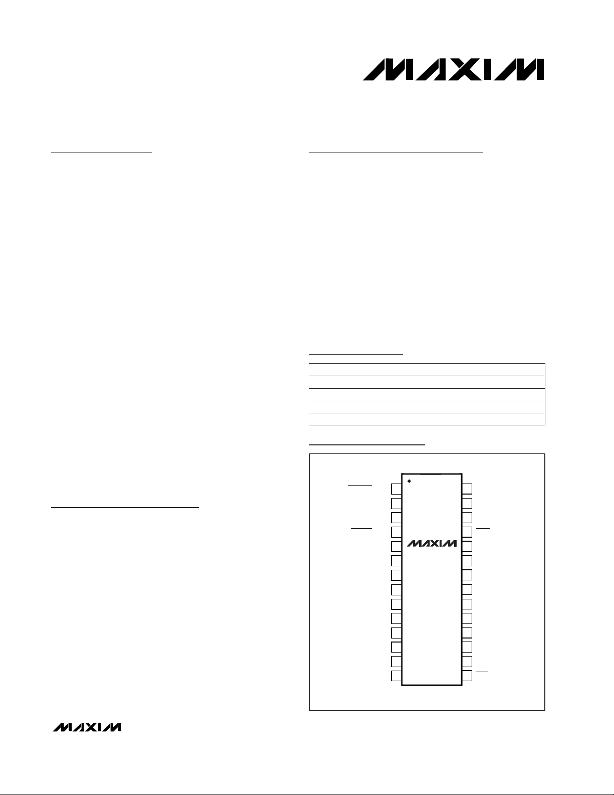
SSOP
TOP VIEW
MAX3130
MAX3131
( ) ARE FOR MAX3131
19-1402; Rev 0; 11/98
PART
MAX3130CAI
MAX3130EAI
MAX3131CAI
0°C to +70°C
-40°C to +85°C
0°C to +70°C
TEMP. RANGE PIN-PACKAGE
28 SSOP
28 SSOP
28 SSOP
Pin Configuration
Ordering Information
MAX3131EAI -40°C to +85°C 28 SSOP
µA
MAX3130/MAX3131
3V to 5.5V, IrDA Infrared Transceiver with
Integrated RS-232 Interface
2 _______________________________________________________________________________________
ABSOLUTE MAXIMUM RATINGS
ELECTRICAL CHARACTERISTICS
(VCC= AVCC= 3.0V to 5.5V, GND = AGND = PGND, C1–C4 = 0.1µF (Note 1), TA= T
MIN
to T
MAX
, unless otherwise noted. Typical
values are at T
A
= +25°C and VCC= AVCC= 3.3V.)
Stresses beyond those listed under “Absolute Maximum Ratings” may cause permanent damage to the device. These are stress ratings only, and functional
operation of the device at these or any other conditions beyond those indicated in the operational sections of the specifications is not implied. Exposure to
absolute maximum rating conditions for extended periods may affect device reliability.
VCCto GND..............................................................-0.3V to +6V
AV
CC
to AGND.........................................................-0.3V to +6V
V
CC
to AVCC.......................................................................±0.3V
AGND, PGND to GND ........................................................±0.1V
V+ to GND................................................................-0.3V to +7V
V- to GND.................................................................+0.3V to -7V
V+ to V-................................................................................+13V
Inputs (referenced to GND)
T1IN, T2IN, TXD,
RSSD, IRMODE, BAUD16,
IRSD....................................................................-0.3V to +6V
R1IN, R2IN .....................................................................±25V
Outputs (referenced to GND)
T1OUT, T2OUT............................................................±13.2V
R1OUT, R2OUT, EDGEDET, RXD.........-0.3V to (V
CC
+ 0.3V)
LEDC...................................................................-0.3V to +6V
Output Short-Circuit Duration (to V
CC
or GND)
T1OUT, T2OUT.....................................................Continuous
Output Currents
LEDC Continuous........................................................200mA
LEDC 20% Duty Cycle t
ON
< 90µs..............................500mA
Input Current
PINC..............................................................................10mA
Continuous Power Dissipation (T
A
= +70°C)
SSOP (derate 9.52mW/°C above +70°C)...................762mW
Operating Temperature Ranges
MAX3130/MAX3131CAI ....................................0°C to +70°C
MAX3130/MAX3131EAI..................................-40°C to +85°C
Storage Temperature Range.............................-65°C to +160°C
Lead Temperature (soldering, 10sec).............................+300°C
±0.01 ±1.0
2.4
120 200
Output Voltage Low I
SINK
= 1.6mA
0.25 1.0
0.1 0.4 V
Output Voltage High I
SOURCE
= 1.0mA
VCC-VCC-
0.6 0.05
V
2.0
0.8
1.0 10
0.01 1.0
MIN TYP MAX
Data Rate (Note 3)
µAVIN= 0 to V
CC
Input Leakage Current
2.4 115.2
VCC= AVCC= 5V
kbps
Equivalent Input Noise Current 10 nA
RMS
Input Current Sensitivity (Note 3) 0.0002 6 mA
Ambient Photodiode Current
Rejection
AVCC= 3.3V 100
AVCC= 5V 375
µA
V
VCC= AVCC= 3.3V
Input Logic Threshold High
VInput Logic Threshold Low
µATA= +25°C (Note 2)Analog Power-Supply Current
mAVCC= 3.3V or 5V, TA= +25°C (Note 2)Power-Supply Current
RSSD = low or IRMODE = low,
T
A
= +25°C (Note 2)
Shutdown Supply Current µA
µA
IRSD = low, TA= +25°C (Note 2)
Shutdown Analog Supply Current
UNITSCONDITIONSPARAMETER
LOGIC INPUTS (T1IN, T2IN, TXD, IRMODE, BAUD16, IRSD, RSSD)
DC CHARACTERISTICS
LOGIC OUTPUTS (R1OUT, R2OUT, RXD, EDGEDET)
IR RECEIVER
MAX3130/MAX3131
3V to 5.5V, IrDA Infrared Transceiver with
Integrated RS-232 Interface
_______________________________________________________________________________________ 3
ELECTRICAL CHARACTERISTICS (continued)
(VCC= AVCC= 3.0V to 5.5V, GND = AGND = PGND, C1–C4 = 0.1µF (Note 1), TA= T
MIN
to T
MAX
, unless otherwise noted. Typical
values are at T
A
= +25°C and VCC= AVCC= 3.3V.)
Data rate = 2.4kbps
Data rate = 115kbps
AVCC= 3.3V
IR Receiver Disable Time Delay until I
AVCC
< 1µA 10 µs
IR Receiver Enable Time Delay until maximum IR receive data rate is valid 300 µs
IR Receiver Output Pulse Width
BAUD16 = static
(Note 3)
190
µs
AVCC= 5V
1 1.6 8
IR TRANSMITTER
Transmitter Rise Time 10% to 90% of 200mA drive current 20 600 ns
Transmitter Fall Time 90% to 10% of 200mA drive current 20 600 ns
Transmitter Output Resistance I
OUT
= 200mA
1.15 2
Ω
0.9 1.6
µs
Off-Leakage Current
1.43 2.23
V
LEDC
= 5.5V
t
PHL
t
PLH
0.01 10.0 µA
IrDA ENCODER/DECODER (ENDEC)
Maximum Operating Frequency Maximum frequency at BAUD16 2 MHz
IR Output Pulse Width f
BAUD16
= 1.8432MHz, measured at V
LEDC
BAUD16 Operating Frequency Range f
BAUD16
required to enable ENDEC 34.6 2000 kHz
RS-232 RECEIVER
Input Voltage Range -25 25 V
Input Threshold Low
VCC= 3.3V 0.6 1.2
V
VCC= 5V 0.8 1.5
Input Threshold High
VCC= 3.3V 1.5 2.4
V
VCC= 5V 1.8 2.4
Input Hysteresis 0.3 V
Input Resistance TA= +25°C 357kΩ
Receiver Propagation Delay
R_IN to R_OUT,
CL= 150pF
300
ns
300
Receiver Skew
t
PHL
- t
PLH
, C
L
= 150pF
300 ns
RS-232 TRANSMITTER OUTPUTS
Output Voltage Swing T1OUT, T2OUT, loaded with 3kΩ to GND ±5 ±5.4 V
Output Resistance VCC= V+ = V- = 0, T_OUT = ±2V 300 10M Ω
Output Short-Circuit Current V
T_OUT
= 0 ±35 ±60 mA
Output Leakage Current
V
T_OUT
= ±12V, VCC= 0 to 5.5V,
RS-232 transceiver shutdown
±25 µA
Maximum Data Rate RL= 3kΩ, CL = 1000pF, one transmitter switching 120 235 kbps
Transmitter Skew
t
PHL
- t
PLH
300 ns
PARAMETER CONDITIONS MIN TYP MAX UNITS
IR TRANSMITTER
IrDA ENCODER/DECODER (ENDEC)
RS-232 RECEIVER
RS-232 TRANSMITTER OUTPUTS
MAX3130/MAX3131
3V to 5.5V, IrDA Infrared Transceiver with
Integrated RS-232 Interface
4 _______________________________________________________________________________________
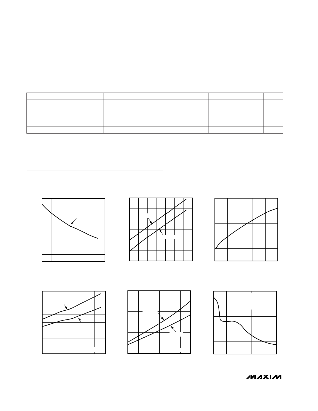
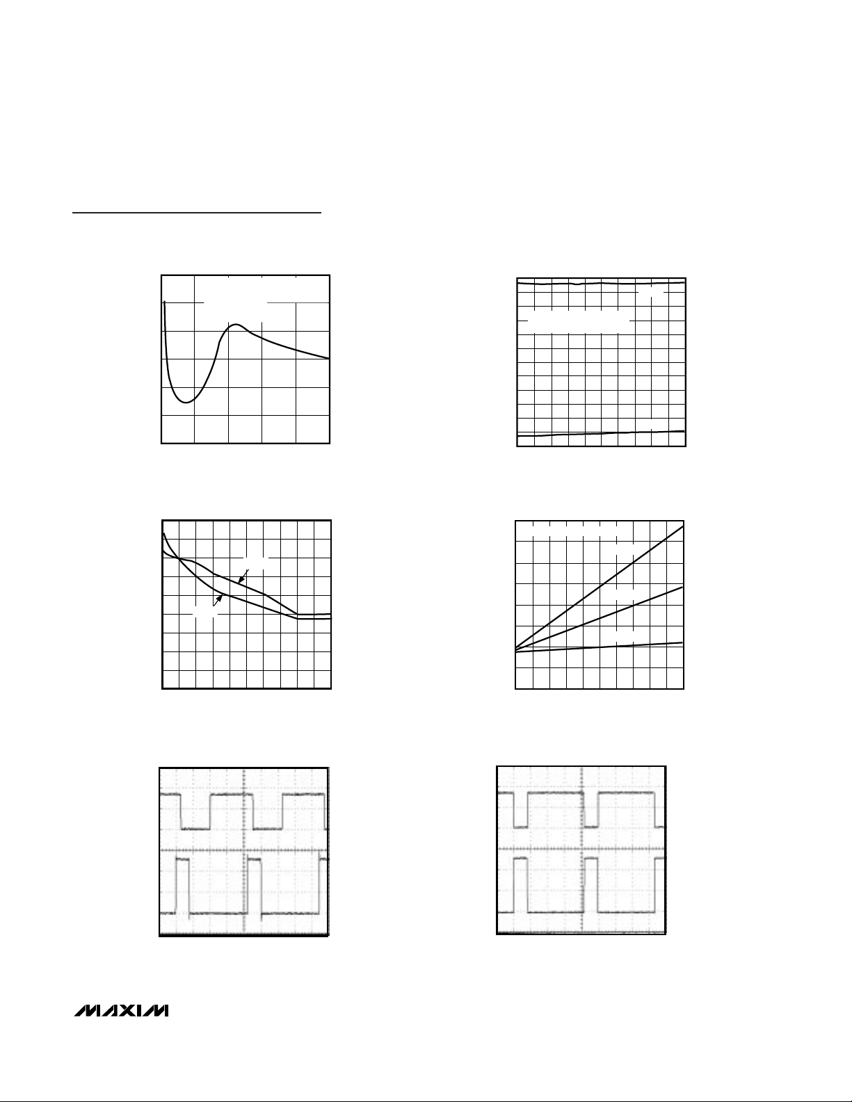
Typical Operating Characteristics
(VCC= AVCC= 3.3V, GND = AGND = PGND, C1–C4 = 0.1µF, RL= 3kΩ, TA = +25°C, unless otherwise noted.)
200
240
220
300
280
260
360
340
320
380
-40 0 20-20 40 60 80 100
SUPPLY CURRENT vs. TEMPERATURE
MAX3130 toc01
TEMPERATURE (°C)
I
CC
(µA)
VCC = 3.3V or 5V
90
110
100
130
120
140
150
-40 20 40-20 0 60 80 100
ANALOG SUPPLY CURRENT
vs. TEMPERATURE
MAX3130 toc02
TEMPERATURE (°C)
I
AVCC
(µA)
AVCC = 5V
AVCC = 3.3V
0
100
300
200
400
500
3.0 4.03.5 4.5 5.0 5.5
AMBIENT PHOTODIODE CURRENT
REJECTION vs. SUPPLY VOLTAGE
MAX3130 toc03
SUPPLY VOLTAGE (V)
CURRENT REJECTION (µA)
0
0.2
0.4
0.6
0.8
1.0
1.2
1.4
1.6
-40 0-20 20 40 80 100
LED DRIVER ON-RESISTANCE
vs. TEMPERATURE
MAX3130 toc04
TEMPERATURE (°C)
R
LED
(Ω)
VCC = 3.3V
VCC = 5V
I
LEDC
= 200mA
0
200
100
400
300
500
600
100 200 250150 300 350 400
LEDC VOLTAGE vs. LEDC CURRENT
MAX3130 toc05
LEDC CURRENT (mA)
LEDC VOLTAGE (mV)
PULSED AT
20% DUTY CYCLE
VCC = 3.3V
VCC = 5V
0
20
60
40
80
100
04020 60 80 100
RXD OUTPUT PULSE WIDTH
vs. DISTANCE (2400bps)
MAX3130 toc06
DISTANCE (cm)
RXD PULSE WIDTH (µs)
TRANSMITTER POWER = 200mW/sr
INPUT PULSE WIDTH = 78µs
TEMIC BPV22NF
V
CC
= 3.3V
Note 1: C1–C4 = 0.1µF, tested at +3.3V ±10%. C1 = 0.047µF, C2–C4 = 0.33µF, tested at +5.0V ±10%.
Note 2: All supply current measurements are made under no-load condition on all outputs, and all input voltages are at V
CC
or GND.
Note 3: For a compliant IrDA input signal where the data rate is within the supported data rate for the IR receive mode: rise/fall
times are less than 600ns and pulse widths are between 1.41µs and 3/16 of the baud rate.
630
MIN TYP MAX
VCC= 3.3V, RL= 3kΩ to
7kΩ, measured from
+3V to -3V or -3V to +3V,
TA = +25°C
Transition-Region Slew Rate V/µs
UNITSCONDITIONSPARAMETER
100Delay until transmitter outputs are validTransmitter Enable Time µs
CL= 150pF to 1000pF
CL= 150pF to 2500pF 430
ELECTRICAL CHARACTERISTICS (continued)
(VCC= AVCC= 3.0V to 5.5V, GND = AGND = PGND, C1–C4 = 0.1µF (Note 1), TA= T
MIN
to T
MAX
, unless otherwise noted. Typical
values are at T
A
= +25°C and VCC= AVCC= 3.3V.)
MAX3130/MAX3131
3V to 5.5V, IrDA Infrared Transceiver with
Integrated RS-232 Interface
_______________________________________________________________________________________
5
1.0
2.0
1.5
3.0
2.5
3.5
4.0
04020 60 80 100
RXD OUTPUT PULSE WIDTH vs. DISTANCE
(115.2 kbps)
MAX3130 toc07
DISTANCE (cm)
RXD PULSE WIDTH (µs)
TRANSMITTER POWER = 200mW/sr
INPUT PULSE WIDTH = 1.63µs
TEMIC BPV22NF
V
CC
= 3.3V
-6
-5
-4
-3
-2
-1
0
1
2
3
4
5
6
0
TRANSMITTER OUTPUT VOLTAGE
vs. LOAD CAPACITANCE
MAX3130 toc08
LOAD CAPACITANCE (pF)
TRANSMITTER OUTPUT VOLTAGE (V)
2000 30001000 4000 5000
V
OUT
+
1 TRANSMITTER AT 235kbps
1 TRANSMITTER AT 15kbps
V
OUT
-
0
4
2
8
6
10
12
16
14
18
0 1000 2000 3000 4000 5000
RS-232 TRANSMITTER SLEW RATE
vs. LOAD CAPACITANCE
MAX3130 toc09
LOAD CAPACITANCE (pF)
SLEW RATE (V/µs)
-SLEW
+SLEW
0
5
10
15
20
25
30
35
40
0
SUPPLY CURRENT vs. LOAD CAPACITANCE
(RS-232 TRANSMITTING)
MAX3130-toc10
LOAD CAPACITANCE (pF)
I
CC
(mA)
2000 30001000 4000 5000
235kbps
1 TRANSMITTER DRIVEN ONLY
120kbps
20kbps
2V/div
2V/div
RXD OUTPUT
vs. INFRARED INPUT
MAX3130 toc11
2µs/div
RXD
OUTPUT
INFRARED
INPUT
V
CC
= 3.3V, 115.2kbps AT 1cm DISTANCE
TEMIC BPV22NF
TRANSMIT POWER 200mW/sr
2V/div
2V/div
RXD OUTPUT
vs. INFRARED INPUT
MAX3130 toc12
100µs/div
RXD
OUTPUT
INFRARED
INPUT
V
CC
= 3.3V, 2400bps AT 1cm DISTANCE
TEMIC BPV22NF
TRANSMIT POWER 200mW/sr
Typical Operating Characteristics (continued)
(VCC= AVCC= 3.3V, GND = AGND = PGND, C1–C4 = 0.1µF, RL= 3kΩ, TA = +25°C, unless otherwise noted.)

MAX3130/MAX3131
3V to 5.5V, IrDA Infrared Transceiver with
Integrated RS-232 Interface
6 _______________________________________________________________________________________
2V/div
2V/div
RXD OUTPUT
vs. INFRARED INPUT
MAX3130 toc15
2µs/div
RXD
OUTPUT
INFRARED
INPUT
V
CC
= 3.3V, 115.2kbps AT 1m DISTANCE
TEMIC BPV22NF
TRANSMIT POWER 200mW/sr
2V/div
2V/div
RXD OUTPUT
vs. INFRARED INPUT
MAX3130 toc16
100µs/div
RXD
OUTPUT
INFRARED
INPUT
V
CC
= 3.3V, 2400bps AT 1m DISTANCE
TEMIC BPV22NF
TRANSMIT POWER 200mW/sr
Pin Description
Typical Operating Characteristics (continued)
(VCC= AVCC= 3.3V, GND = AGND = PGND, C1–C4 = 0.1µF, RL= 3kΩ, TA = +25°C, unless otherwise noted.)
2V/div
2V/div
RXD OUTPUT
vs. INFRARED INPUT
MAX3130 toc13
2µs/div
RXD
OUTPUT
INFRARED
INPUT
V
CC
= 3.3V, 115.2kbps AT 10cm DISTANCE
TEMIC BPV22NF
TRANSMIT POWER 200mW/sr
2V/div
2V/div
RXD OUTPUT
vs. INFRARED INPUT
MAX3130 toc14
100µs/div
RXD
OUTPUT
INFRARED
INPUT
V
CC
= 3.3V, 2400bps AT 10cm DISTANCE
TEMIC BPV22NF
TRANSMIT POWER 200mW/sr
MAX3131MAX3130
PIN
1 IR Receiver TTL/CMOS Data OutputRXD—
—
Edge Detector Output. EDGEDET goes low if activity is sensed on either the RS-232
receiver or the IrDA receiver, depending on the state of IRMODE. See
EDGEDET: Edge-
Detection Circuitry
section.
EDGEDET
1
2 TTL/CMOS RS-232 Transmitter InputT1IN2
FUNCTIONNAME

MAX3130/MAX3131
3V to 5.5V, IrDA Infrared Transceiver with
Integrated RS-232 Interface
_______________________________________________________________________________________ 7
Pin Description (continued)
TTL/CMOS RS-232 Receiver Output. For the MAX3130, drive IRMODE low to connect
R2OUT to the IR receiver output, and drive IRMODE high to connect R2OUT to the
RS-232 receiver output. For the MAX3131, R2OUT is always internally connected to the
RS-232 receiver output.
R2OUT2828
RS-232 Receiver InputR2IN2727
RS-232 Transmitter OutputT2OUT2626
Shutdown Input for the RS-232 Transmitters and Charge Pump
RSSD
2525
-5.5V Generated by the Internal Charge PumpV-2424
Negative Terminal of the Inverting Charge-Pump CapacitorC2-2323
Positive Terminal of the Inverting Charge-Pump CapacitorC2+2222
Negative Terminal of the Voltage-Doubling Charge-Pump CapacitorC1-2121
Positive Terminal of the Voltage-Doubling Charge-Pump CapacitorC1+2020
Shutdown Input for the IrDA Transceiver Circuitry
IRSD
1515
Analog Ground for IR Signal Processing. Connect to GND.AGND1313
Analog Supply Voltage VCCfor IR Signal Processing. AVCCrange is 3.0V to 5.5V.AV
CC
1212
Silicon PIN Photodiode Input. Connect PINC to the cathode of the PIN photodiode.
Connect the anode of the PIN photodiode to GND.
PINC1414
Open-Drain Output for Driving the IR LED. Connect LEDC to the cathode of the IR LED.LEDC1717
Power Ground for IR LED Driver. Connect to GND.PGND1616
+5.5V Generated by the Internal Charge PumpV+1919
No Connection. Do not make connections to these pins.
N.C.11, 1811, 18
6
7
8
9
10
MAX3131
3
4
5
MAX3130
PIN
RS-232 Receiver InputR1IN6
RS-232 Transmitter OutputT1OUT7
16-Times Baud-Rate Input. To use the ENDEC, apply a signal that is 16 times the baud
rate into BAUD16. Connect BAUD16 to GND or VCCto disable the ENDEC.
BAUD168
GroundGND9
3.0V to 5.5V Supply VoltageV
CC
10
TTL/CMOS RS-232 Transmitter Input. For the MAX3130, drive IRMODE low to connect
T2IN to the IR transmitter input, and drive IRMODE high to connect T2IN to the RS-232
transmitter input. For the MAX3131, T2IN is always connected to the RS-232 transmitter
input.
T2IN3
IR Transmitter TTL/CMOS Data InputTXD—
TTL/CMOS RS-232 Receiver OutputR1OUT5
FUNCTIONNAME
—
IR Mode Control. Drive IRMODE low to connect R2OUT to the IR receiver output and
T2IN to the IR transmitter input. Driving IRMODE low also shuts down the RS-232
charge pump and puts the RS-232 transmitter outputs in a high-impedance state. Drive
IRMODE high to connect R2OUT to the RS-232 receiver output and connect T2IN to the
RS-232 transmitter input.
IRMODE
4

MAX3130/MAX3131
3V to 5.5V, IrDA Infrared Transceiver with
Integrated RS-232 Interface
8 _______________________________________________________________________________________
Detailed Description
The MAX3130/MAX3131 are IrDA 1.2 compatible,
infrared transceivers with an integrated RS-232 interface. By selecting appropriate external optical components, these devices support IrDA 1.2 data rates from
2.4kbps to 115kbps at distances from 1cm to 1m. A
low-noise design allows them to achieve a bit-error rate
below 10-8at maximum data rates. On-chip filtering
rejects out-of-band ambient light signals that interfere
with infrared communication. Both devices include a
high-power LED driver capable of sinking 200mA.
The MAX3130 and MAX3131 contain two RS-232 drivers
and two RS-232 receivers that support data rates up to
120kbps. The RS-232 transceiver is powered by a highefficiency, dual charge-pump power supply that operates with input supply voltages from +3.0V to +5.5V.
The MAX3130 is optimized for applications using a single UART for both infrared and RS-232 communication.
The infrared transmitter input and infrared receiver output are multiplexed with one RS-232 transmitter input
and one RS-232 receiver output, respectively. The
MAX3131 IrDA and RS-232 transceivers are independent of each other for use in simultaneous multiprotocol
transceiver applications.
IR Receivers
The receiver amplifier reverse biases the PIN diode
with approximately 1.2V, and the PIN diode converts
pulses of IR light into pulses of current. The input transimpedance (current-to-voltage) amplifier converts and
amplifies these current pulses into voltage pulses. The
MAX3130/MAX3131 incorporate filters that remove lowfrequency ambient light interference and high-frequency
circuit noise from these voltage pulses. A high-speed
comparator then translates these voltage pulses into
CMOS output levels. Figures 1 and 2 show system
functional diagrams.
The RXD pin is the output of the infrared receiver for
the MAX3131. The R2OUT pin is the output of the
infrared receiver for the MAX3130 (IRMODE = low).
With the ENDEC disabled, the infrared receiver output
pulses low upon each incoming infrared pulse. The
pulse width of the receiver output depends on many
factors, including transmitter distance and power, PIN
photodiode efficiency and area, and incoming data
rate. Under all circumstances the output pulse is less
than one baud period. To communicate with UARTs
that are not IrDA compatible, enable the ENDEC (see
the
IrDA Encoder/Decoder (ENDEC)
section).
MAX3131 Operational Modes Table
RSSD IRSD
T_OUT R_IN LEDC RXD
0 0 High-Z Enabled Enabled Logic High
0 1 High-Z Enabled Enabled IrDA Output
1 0 Enabled Enabled Enabled Logic High
1 1 Enabled Enabled Enabled IrDA Output
MAX3130 Function Table
RSSD
X
X 0
0
IRMODE
MAX3130
CONTROL INPUTS
IRSD
0
1
RS-232
Input
RS-232
Input
T1IN
LOGIC INPUTS
IrDA
Input
IrDA
Input
T2IN
EnabledHigh-Z
High-Z
T1OUT
RS-232 I/O
High-Z
High-Z
T2OUT
Disabled
RS-232
Input
RS-232
Input
R1IN PINC
RS-232
Input
RS-232
Input
R2IN
IrDA
INPUT
RS-232
Output
RS-232
Output
R1OUT
LOGIC OUTPUTS
IrDA
Output
IrDA
Output
R2OUT
Disabled
Enabled
Enabled
LEDC
IrDA
OUTPUT
0 1 0
RS-232
Input
RS-232
Input
High-Z High-Z
RS-232
Input
RS-232
Input
RS-232
Output
RS-232
Output
Disabled
0 1 1
RS-232
Input
RS-232
Input
High-Z High-Z
RS-232
Input
RS-232
Input
RS-232
Output
RS-232
Output
Disabled Enabled
Disabled
Enabled
1 1 0
RS-232
Input
RS-232
Input
RS-232
Output
RS-232
Output
RS-232
Input
RS-232
Input
RS-232
Output
RS-232
Output
Disabled
1 1 1
RS-232
Input
RS-232
Input
RS-232
Output
RS-232
Output
RS-232
Input
RS-232
Input
RS-232
Output
RS-232
Output
Disabled
X = Don’t care

MAX3130/MAX3131
3V to 5.5V, IrDA Infrared Transceiver with
Integrated RS-232 Interface
_______________________________________________________________________________________ 9
MAX3130
EDGE
EDGE
Rx
RxIN
TxIN
Tx
ENDEC
CHARGE PUMP
SHDN
1µF
R
SET
GND
V
CC
1µF
AGND
AV
CC
EDGEDET
T2OUT
R2IN
R1IN
RSSD
V+
V-
LEDC
PGND
PINC
1.2V
C4
C3
T1OUT
RS-232
INPUTS
RS-232
OUTPUTS
OFF
ON
IR
232
OFF
ON
RECEIVE
LOGIC
OUTPUTS
TRANSMIT
LOGIC
INPUTS
C1+
C1
C1-
C2+
C2
C2-
IRSD
BIAS
5k
5k
BAUD16
IRMODE
R1OUT
R2OUT
T1IN
T2IN
f
BAUD16
Figure 1. MAX3130 Functional Diagram

MAX3130/MAX3131
3V to 5.5V, IrDA Infrared Transceiver with
Integrated RS-232 Interface
10 ______________________________________________________________________________________
MAX3131
Rx
RxIN
TxIN
Tx
ENDEC
CHARGE PUMP
1µF
R
SET
GND
V
CC
1µF
AGND
AV
CC
PINC
PGND
LEDC
R2IN
R1IN
V-
C4
C3
T1OUT
T2OUT
RS-232
INPUTS
RS-232
OUTPUTS
OFF
ON
OFF
ON
RS-232
RECEIVE
LOGIC
OUTPUTS
IrDA RECEIVE
LOGIC
OUTPUT
RS-232
TRANSMIT
LOGIC
INPUTS
IrDA TRANSMIT
LOGIC INPUT
C1+
C1
C2
C1-
C2+
C2-
IRSD
BIAS
5k
5k
BAUD16
R1OUT
R2OUT
T1IN
T2IN
TXD
RXD
f
BAUD16
V+
RSSD
SHDN
1.2V
Figure 2. MAX3131 Functional Diagram

MAX3130/MAX3131
3V to 5.5V, IrDA Infrared Transceiver with
Integrated RS-232 Interface
______________________________________________________________________________________ 11
IR Transmitter
The infrared transmitter consists of an internal highpower, open-drain MOSFET switch. This switch has an
on-resistance of less than 2Ω and is capable of switching 200mA of current. Internal buffering keeps the input
capacitance of the TXD pin extremely low to ease user
drive requirements. Connect an IR LED in series with a
current-setting resistor to select the appropriate IR output power (see the
Powering the IR LED
section). The
transmitter is not current limited so do not exceed the
power dissipation of the external components during
high duty-cycle transmit schemes.
The TXD input controls the IR LED for the MAX3131.
The T2IN input controls the IR LED for the MAX3130
(IRMODE = low). With the ENDEC disabled (see
IrDA
Encoder/Decoder (ENDEC)
section), the IR LED is
turned on by a logic-high signal at the TXD or T2IN
input, for the MAX3131 and MAX3130 respectively.
IRMODE
: Multiplexed RS-232 Operation
and IrDA Operation (MAX3130)
The MAX3130 has the capability to multiplex R2OUT and
T2IN between the IrDA infrared interface and the RS-232
electrical interface. The state of the IRMODE input determines which interface (infrared or RS-232) is multiplexed
to R2OUT and T2IN. When IRMODE is low, R2OUT acts
as the infrared receiver output and T2IN acts as the
infrared transmitter input. Also, while IRMODE is low, the
RS-232 charge pumps are shut down and the RS-232
transmitters are disabled (see
Shutdown
section). When
IRMODE is high, R2OUT and T2IN assume their functions as the RS-232 data receive output and transmit
input, respectively. Also, while IRMODE is high, the IR
transmitter is disabled (turned off).
EDGEDET
: Edge-Detection Circuitry
(MAX3130)
The MAX3130 has internal edge-detection circuitry that
monitors the RS-232 R2OUT line when IRMODE is low
and monitors the IrDA receive channel when IRMODE
is high. EDGEDET goes low when a positive or negative
edge is detected on either the RS-232 R2OUT line or
the IrDA receive channel (depending on the IRMODE
pin). This edge-detection feature is useful for initiating
an interrupt when data is received on the deselected
line. The EDGEDET signal is cleared when IRMODE is
toggled. Table 1 shows EDGEDET operation.
IrDA Encoder/Decoder (ENDEC)
The MAX3130 and MAX3131 provide an on-board
ENDEC to communicate with UARTs that are not IrDA
compatible. The ENDEC is enabled by applying a clock
with a frequency 16 times the baud rate to the BAUD16
input. This BAUD16 clock is commonly provided on
UARTs that do not have IrDA ENDEC capability. Figure
3 illustrates the operation of the ENDEC. The ENDEC
stretches the incoming infrared pulse (a pulse between
IRSD RSSD IRMODE
R2IN IrDA RxIN
EDGEDET*
X X 0 X
X X 0 X
X X 1 X
X X 1 X
Table 1. EDGEDET Operation
1.41µs < t < 3CS
16CS 32CS
16CS
R2OUT (RXD)
WITH ENDEC ENABLED
R2OUT (RXD)
WITH ENDEC DISABLED
CS = BAUD16 CLOCK CYCLES
* HIGH = INFRARED LIGHT PULSE
( ) ARE FOR MAX3131
INFRARED
PHOTODIODE INPUT *
Figure 3a. ENDEC Operation, Receiving Infrared
X
= Don’t care
*
EDGEDET is cleared by any transition on IRMODE.

MAX3130/MAX3131
3V to 5.5V, IrDA Infrared Transceiver with
Integrated RS-232 Interface
12 ______________________________________________________________________________________
3CS
7CS
16CS
T2IN (TXD)
CS = BAUD16 CLOCK CYCLES
* HIGH = INFRARED LIGHT PULSE
( ) ARE FOR MAX3131
INFRARED LED
OUTPUT *
Figure 3b. ENDEC Operation, Transmitting Infrared
LapLink is a trademark of Traveling Software.
1µs and three BAUD16 clock cycles) into a full baud
period (Figure 3a). Signals applied to TXD are inverted
and compressed to three BAUD16 clock cycles by the
ENDEC before being transmitted (Figure 3b). The
ENDEC is disabled by connecting the BAUD16 input to
VCCor GND.
Dual Charge-Pump Voltage Converter
The MAX3130/MAX3131’s internal power supply consists of a regulated dual charge pump that provides
output voltages of +5.5V (doubling charge pump) and
-5.5V (inverting charge pump) for supply voltages from
+3.0V to +5.5V. The charge pump operates in a discontinuous mode: if the output voltages are less than
5.5V, the charge pumps are enabled; if the output voltages exceed 5.5V, the charge pumps stop switching.
Each charge pump requires a flying capacitor (C1, C2)
and a reservoir capacitor (C3, C4) to generate the V+
and V- supplies (Figures 1 and 2). If RSSD (or IRMODE
for MAX3130) is low, both charge pumps shut down.
RS-232 Transmitters
The RS-232 transmitters are inverting level translators
that convert CMOS-logic levels to ±5.0V EIA/TIA-232
levels. The MAX3130/MAX3131 transmitters are guaranteed for data rates of 120kbps, providing compatibility with PC-to-PC communication software, such as
LapLink™. These RS-232 transmitters typically operate
at data rates of 235kbps. The RS-232 transmitter outputs are high impedance when either IRMODE or RSSD
are low.
The MAX3130/MAX3131 RS-232 receivers translate RS232 signal levels to CMOS-level logic. The RS-232
receivers also perform a logic inversion from input to
output. The receivers are always active and are not
affected by the RS-232 shutdown input (RSSD).
__________ Applications Information
Shutdown
The MAX3130/MAX3131 have split analog and digital
supplies (VCCand AVCC) with separate shutdown
modes. When IRSD is pulled low, the IR receiver is disabled and AVCCcurrent reduces to <1µA. When RSSD
or IRMODE is pulled low, the RS-232 charge pumps
are disabled and the RS-232 transmitter outputs
become high impedance. In this mode, the VCCcurrent
reduces to <10µA.
IR LED Selection
The IrDA specification calls for an IR transmitter with a
peak wavelength between 850nm and 900nm. Within a
±15° half-cone angle, the output intensity of the IR LED
must be between 40mW/sr and 500mW/sr. Outside a
±30° half-cone angle, the output intensity of the IR LED
must fall below 40mW/sr. Within these cases, the optical rise and fall times of the IR LED must be less than
600ns. Based on these system requirements the HP
HSDL-4220, the Temic TSHF5400, or equivalent IR
LEDs are appropriate choices.
Powering the IR LED
Set the current in the IR LED with an external resistor.
Using the IR LED manufacturer’s data sheet, select a
forward current that meets the IrDA specifications discussed in the
IR LED Selection
section. Determine the
forward bias voltage of the IR LED (V
IRLED
) and the
voltage drop across the MAX3130/MAX3131 LED driver
(see LEDC Voltage vs. LEDC Current graph in the
Typical Operating Characteristics
) and choose the cur-
rent-setting resistor based on the following equation:
R
SET
= (VCC- V
IRLED
- V
LEDC
) / I
SET
Using the HP HSDL-4220 IR LED as an example:
VCC= 5V, I
SET
= 100mA, V
IRLED
= 1.67V
V
LEDC
= 90mV
R
SET
= (5V - 1.67V - 90mV) / 0.1A = 32.4Ω

MAX3130/MAX3131
3V to 5.5V, IrDA Infrared Transceiver with
Integrated RS-232 Interface
______________________________________________________________________________________ 13
Power dissipation of the MAX3130/MAX3131, IR LED,
and R
SET
are based on the maximum LED current and
duty cycle.
Use the following equations to calculate the power dis-
sipation in each component:
MAX3130 power dissipation = I
SET
· V
DRV
· duty cycle
IR LED power dissipation = I
SET
· V
IRLED
· duty cycle
R
SET
power dissipation = I
SET
2
· R
SET
· duty cycle
For reliable operation, do not exceed maximum power
dissipation of the components.
PIN Photodiode Selection
PIN photodiode selection is extremely important to system performance. The PIN diode must generate at least
200nA (minimum sensitivity of the MAX3130/MAX3131)
of current when aimed ±15° off-axis with an incident
irradiance of 4µW/cm2. The following equation determines if the Temic BPV22NF meets these requirements:
I
PIN
= (4µW/cm2) (0.075cm2) (0.95) (0.95) (1.8) (0.6A/W)
= 292nA
The first term (4mW/cm2) is the minimum guaranteed
irradiance in the ±15° angular range. The second term
(0.075cm2) is the sensitive area of the PIN diode. The
first 0.95 factor normalizes the sensitivity to the 875nm
wavelength and the second 0.95 factor adjusts for the
decreased receiver efficiency at ±15° off-axis. The 1.8
factor accounts for the round lens which increases the
effective PIN diode area. The last term (0.6A/W) is the
sensitivity of the PIN diode. Based on this example, the
Temic BPV22NF is an appropriate selection.
The final important factor in selecting a PIN diode is the
effective diode capacitance. It is important to keep this
capacitance below 70pF at 1.2V reverse bias. Higher
input capacitance compromises the noise performance
of the system by increasing the noise gain of the input
transimpedance amplifier.
Capacitor Selection
The capacitor type used for C1–C4 is not critical for
proper operation; either polarized or nonpolarized
capacitors are good choices. The charge pump
requires 0.1µF capacitors for 3.3V operation. For other
supply voltages, refer to Table 2 for suggested capacitor values. Do not use values smaller than those listed
in Table 2. Increasing the capacitor values (e.g., by a
factor of 2) reduces ripple on the transmitter outputs
and slightly reduces power consumption. C2, C3, and
C4 can be increased without changing C1’s value.
However, do not increase C1 without also increasing the values of C2, C3, and C4.
When using the minimum required capacitor values,
make sure the capacitor value does not degrade
excessively with temperature. If in doubt, use capacitors with a larger nominal value. The capacitor’s equivalent series resistance (ESR) usually rises at low
temperatures and increases the amount of ripple on V+
and V-.
Power-Supply Noise Rejection
Because of the extremely sensitive nature of photodiode amplifiers, it is important to maintain a low-noise
supply voltage. Use a separate analog supply voltage
where possible. Place a 1µF ceramic bypass capacitor
as close as possible to the AVCCand VCCpins. In
especially noisy systems, connect a small (10Ω) resistor in series with VCC, in addition to the normal bypass
capacitors.
IrDA or RS-232 Application Circuit
Figure 4 shows how the MAX3130 is used to multiplex
between RS-232 and IrDA communication while using
only one UART. By using the IRMODE input, the type of
communication (infrared or RS-232) is controlled by the
I/O of a µP. The internal MAX3130 ENDEC is used to
translate between UART-type and IrDA-type bitstreams. If the UART has this capability, connect
BAUD16 of the MAX3130 to GND.
Figure 5 shows the MAX3131 used with two UARTs to
perform simultaneous IrDA and RS-232 communication.
UART1 is a software UART used to perform infrared
IrDA communication. The internal ENDEC on the
MAX3131 translates between UART-type and IrDA-type
bit-streams. The MAX3100 is implemented as UART2
and communicates via the RS-232 interface. The
MAX3100 interfaces to the µP using a SPI interface.
Layout Considerations
The MAX3130/MAX3131 require careful layout techniques to minimize parasitic signals coupling to the
PINC input. Keep the lead length between the photodiode and PINC as short as possible. Keep PC board
traces to the PIN diode away from other noisy traces.
To minimize coupling, run the AGND trace adjacent to
the PINC trace on both sides. To prevent oscillation,
avoid routing the RXD trace near the PINC trace.
Connect the anode of the PIN diode, GND, and the
ground lead of the AVCCbypass capacitor in a starconnection. Keep the output pins RXD and TXD as
short as possible to minimize coupling back to the input
via parasitic capacitance.

MAX3130/MAX3131
3V to 5.5V, IrDA Infrared Transceiver with
Integrated RS-232 Interface
14 ______________________________________________________________________________________
RTS
CTS
Tx
Rx
T1IN
R1OUT
T2IN
R2OUT
TXD
RXD
BAUD16
T1OUT
R1IN
T2OUT
R2IN
LEDC
PINC
MAX3131
MAX3100
UART2
µP
IrDA
RS-232
1 2 3 4 5
6 7 8 9
DB-9
NON-IrDA UART
(UART1)
TX
RX
BAUD16
SPI
DIN
DOUT
SCLK
CS
Figure 5. Using the MAX3131 and Two UARTs to Perform Simultaneous IrDA and RS-232 Communication
Table 2. Required Capacitor Values
STANDARD
NON-IrDA
UART
RTS
CTS
Tx
Rx
BAUD16
T1IN
R1OUT
T2IN
R2OUT
BAUD16
T1OUT
R1IN
T2OUT
R2IN
LEDC
PINC
MAX3130
IRMODE
µP
I/O
232
IrDA
IrDA
RS-232
1 2 3 4 5
6 7 8 9
DB-9
Figure 4. Using the MAX3130 and a Single UART to Perform Both IrDA and RS-232 Communication
VCC(V) C1 (µF) C2, C3, C4 (µF)
3.0 to 3.6 0.1 0.1
4.5 to 5.5 0.047 0.33
3.0 to 5.5 0.1 0.47

MAX3130/MAX3131
3V to 5.5V, IrDA Infrared Transceiver with
Integrated RS-232 Interface
______________________________________________________________________________________ 15
SSOP.EPS
________________________________________________________Package Information
Chip Information
TRANSISTOR COUNT: 1039

MAX3130/MAX3131
3V to 5.5V, IrDA Infrared Transceiver with
Integrated RS-232 Interface
Maxim cannot assume responsibility for use of any circuitry other than circuitry entirely embodied in a Maxim product. No circuit patent licenses are
implied. Maxim reserves the right to change the circuitry and specifications without notice at any time.
16
____________________Maxim Integrated Products, 120 San Gabriel Drive, Sunnyvale, CA 94086 408-737-7600
© 1998 Maxim Integrated Products Printed USA is a registered trademark of Maxim Integrated Products.
NOTES
 Loading...